REVIEW 3 major objections 5 minor 38 references
Two-Dimensional Antimony Oxide
T0 review · 3 major / 5 minor · reviewed 2026-08-14 · deepseek-v4-flash
Pith's one-line read Antimonene oxidation is predicted to yield stable, tunable semiconducting oxide layers.
desk verdict A credible DFT prediction of chainlike type-II antimonene oxides with a tunable 2.0–4.9 eV gap range, but the 4.9 eV upper endpoint rests on a dynamically unstable idealized geometry and needs a follow-up on the relaxed structure. read the letter →
The pith
A machine-rendered reading of the paper's core claim, the machinery that carries it, and where it could break.
The reading
What carries the argument
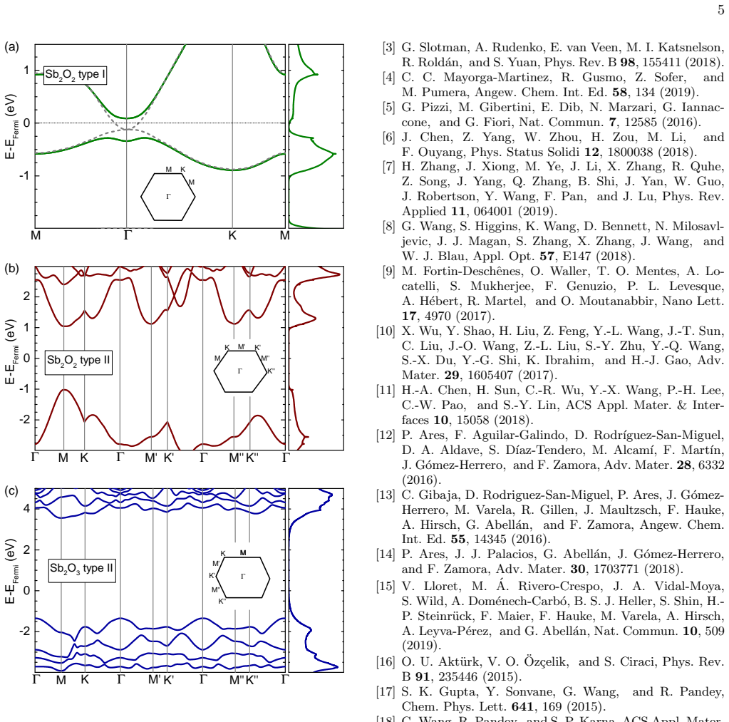
The central object is the type (II) antimonene oxide monolayer: a two-dimensional lattice in which every oxygen bridges two antimony atoms, forming chains of alternating Sb and O that are cross-linked by Sb-Sb or Sb-O-Sb bonds, in place of the perpendicular Sb=O double bonds of type (I). The argument is carried by density functional theory: hybrid-functional (HSE12) band-structure calculations set the gaps, phonon calculations supply the Raman-active frequencies, and the type (II) geometries are generated by displacing atoms along unstable phonon modes of type (I) structures (a frozen-phonon approach) and corroborated by 300 K molecular dynamics in which oxygen atoms enter the antimonene plane. The electronic-structure mechanism is the oxygen content: adding oxygen raises the gap from 2.0 to 4.9 eV and changes the gap from direct to indirect, so the degree of oxidation acts as the tuning parameter.
What would settle it
Compute the HSE12 band structure of the fully relaxed distorted Sb$_2$O$_3$ monolayer (the larger-unit-cell geometry the paper mentions): a gap far from 4.9 eV would remove the upper end of the claimed range. Experimentally, measuring the optical absorption edge of an oxidized single-layer antimonene flake and finding no absorption onset between 2.0 and 4.9 eV would contradict the semiconductor claim.
Extended reading notes
Core claim
The central claim is that air-oxidized antimonene is not a random oxide coating but a family of ordered two-dimensional crystals whose properties follow from stoichiometry and bonding. Specifically, the paper states that all type (II) single-layer antimonene oxides it presents are semiconductors, with direct and indirect band gaps from approximately 2.0 eV (Sb$_2$O$_2$, direct at the zone edge) to 4.9 eV (Sb$_2$O$_3$, indirect), and that these chainlike oxides are energetically preferred over the perpendicular double-bonded type (I) geometry by roughly 3.9 eV (monolayer) and 2.7 eV (bilayer). Type (I) Sb$_2$O$_2$ is instead predicted to be a topological insulator with a small 168 meV gap once spin-orbit coupling is included, matching an earlier proposal. The paper concludes from molecular dynamics that oxygen spontaneously inserts into the antimonene sheet at room temperature, and that the resulting Sb$_2$O$_3$-like layers account for the Raman spectra observed on oxidized few-layer antimonene.
Load-bearing premise
The 4.9 eV upper end of the claimed band-gap range is computed for an idealized Sb$_2$O$_3$ monolayer that the paper itself says is not fully dynamically stable and relaxes into a slightly distorted geometry in a larger unit cell, so the claim depends on that idealized geometry being representative of the real oxidized layer.
Editorial extensions
If this is right
- Type (I) double-bonded antimonene oxides are metastable at best: relaxation to type (II) lowers the monolayer energy by about 3.9 eV and the bilayer energy by about 2.7 eV.
- Oxidation state controls the electronic character: type (II) Sb$_2$O$_2$ is a direct-gap semiconductor near 2.0 eV, Sb$_2$O$_3$ is an indirect-gap semiconductor near 4.9 eV, and few-layer antimonene itself is semimetallic.
- Raman spectroscopy can distinguish the phases: type (I) shows a high-frequency Sb=O stretch near 823 cm$^{-1}$, while type (II) modes fall below about 600 cm$^{-1}$, with Sb$_2$O$_3$ matching published spectra of oxidized few-layer antimonene.
- Natural heterostructures should form: semimetallic antimonene layers sandwiched between semiconducting oxide layers, because antimony reacts readily with oxygen.
- Stoichiometries beyond Sb$_2$O$_3$ are unlikely to be stable as 2D layers, since the antimony atoms available for oxygen bonding are exhausted.
Reading between the lines
- Inference: the oxygen-insertion motif may extend to other pnictogen monolayers such as arsenene or bismuthene, which could form analogous stable oxide layers instead of degrading; this is not asserted by the paper.
- Inference: the upper bound of 4.9 eV rests on an idealized Sb$_2$O$_3$ monolayer that relaxes into a slightly distorted structure in larger cells, so real oxidized flakes may show a range or a lowered effective gap; measuring the optical absorption edge of single oxidized flakes would test this.
- Inference: the distinct Raman frequencies suggest a practical oxidation monitor, watching the disappearance of the type (I) 823 cm$^{-1}$ mode and growth of type (II) modes, which the paper does not explicitly propose.
Signed reviews
Editorial analysis
A structured set of objections, weighed in public.
Referee Report
Summary. The paper proposes a family of two-dimensional antimony oxide structures, termed type (II), in which oxygen atoms are incorporated into the antimonene plane with Sb–O–Sb bridge bonds, in contrast to the type (I) structures with perpendicular Sb=O double bonds. Using DFT total-energy comparisons, phonon calculations, and molecular dynamics, the authors argue that type (II) structures are significantly more stable than type (I) structures, and they report a stoichiometry-dependent band-gap range of approximately 2.0–4.9 eV for type (II) monolayers, computed with the HSE12 hybrid functional. They also provide calculated Raman-active mode frequencies for experimental identification and claim qualitative agreement with Raman spectra of oxidized few-layer antimonene reported in an unpublished companion work.
Significance. If the central claims hold, the paper offers a plausible structural model for the natural oxidation of antimonene, with technologically relevant tunable band gaps and clear spectroscopic fingerprints. The work is significant because it challenges the previously assumed double-bonded oxide structure and provides a concrete alternative that is more stable at the DFT level. Strengths include the internally consistent use of frozen-phonon distortions from calculated unstable modes to construct type (II) structures, the corroborating molecular dynamics simulations, and the explicit energy lowerings (about 3.9 eV for 1L and 2.7 eV for 2L) that make the type (I)-to-type (II) transformation physically plausible. The Raman mode predictions, if anchored to published experimental data, would be practically useful. However, the upper end of the reported band-gap range rests on a dynamically unstable idealized structure, and the key experimental corroboration is an unpublished manuscript with overlapping authorship, so the significance of the headline claims is currently conditional.
major comments (3)
- [Electronic properties, Fig. 4(c) and text near Fig. 1(j)] The central claim of a tunable band-gap range of 2.0–4.9 eV is not fully supported because the 4.9 eV value for the Sb2O3 monolayer is computed for the idealized structure of Fig. 1(j), which the authors themselves state is not fully dynamically stable and relaxes into a slightly distorted geometry in a larger unit cell (Fig. S4). The energy difference of only 5 meV per formula unit does not guarantee that the electronic structure, especially the fundamental gap, is unchanged; the band structure of the stable distorted geometry is not reported. Since the upper endpoint of the headline range is precisely the value that is not anchored to a dynamically stable structure, the authors should either compute and report the band structure of the fully relaxed geometry at the same HSE12 level, or explicitly revise the claimed range to exclude the unstable idealized case. This issue is load-bearing for the paper's main conclusion.
- [Comparison with experiment, Ref. [33] and Raman discussion] The claimed agreement with experimental Raman spectra of oxidized antimonene relies entirely on Ref. [33], which is unpublished and shares several authors with the present manuscript. No experimental spectra, peak positions, or quantitative fitting are shown. As a result, the confirmation loop is not closed: the type (II) structures are presented as consistent with data that the reader cannot independently inspect. The authors should either include the experimental Raman data and a quantitative comparison, or restrict themselves to stating that the predicted modes fall in a plausible range and defer experimental validation to future published work.
- [Trilayer structures and strain, text near Figs. 1(e)-(i)] The trilayer type (II) structures used to motivate the stoichiometries and to illustrate the phase transformation impose up to 17% strain on the inner non-oxidized antimonene layer, as the authors acknowledge. This large strain makes the trilayer geometries physically unrealistic as direct models of oxidized few-layer antimonene. The paper does not examine whether the type (II) motifs survive in larger commensurate supercells with lower strain, nor does it report the electronic or vibrational properties of such relaxed trilayer models. Given that the paper aims to describe few-layer antimonene oxides, this limitation deserves a quantitative treatment or an explicit caveat that only the monolayer and bilayer results are representative.
minor comments (5)
- [Abstract and summary] The abstract states that the structures range "from topological insulators to semiconductors," but no type (II) structure is predicted to be a topological insulator in the manuscript; the only topological-insulator statement concerns the type (I) monolayer in Ref. [22]. The wording should be aligned with the actual content.
- [Fig. 3 caption] The caption says the height of the bars indicates Raman activity on a logarithmic scale, but the axis label "log. Raman activity" and the use of arbitrary units are potentially confusing. Please clarify the normalization and the meaning of the y-axis.
- [Text near Fig. 1] The phrase "Sb2O" is used both as a stoichiometric label and as a structure name; for example, "1L, type (II)" is labeled Sb2O in Fig. 1(f), which is consistent but not defined in the main text. A sentence defining the notation (number of Sb and O atoms per unit cell of one outer layer) would help.
- [References] The manuscript cites "Sec. 5 of the Supplemental Material" for several points, but the Supplemental Material itself is not provided to the reader in the main text and the structure of that document is not described. Please ensure the supplementary document is available and that all cross-references (Fig. S4, S5-S7, S8-S12) are correct.
- [General text] There are minor typographical errors, such as "stochiometry" in the summary and "computational resources used for the calculations" being a sentence fragment. The manuscript should be carefully proofread.
Circularity Check
The only experimental confirmation is an unpublished self-citation; the DFT band-gap and stability predictions are otherwise self-contained.
-
self citation load bearing
[Experimental agreement paragraph (unnumbered, p. 4) and Ref. [33]]
"Reference [33] reports the formation of a passivation layer on the surface, which shows evidence for Sb2O3-like layers. Raman measurements reveal characteristic modes in the range of 190-450 cm−1. This experimentally rules out the formation of type (I) structures. Instead, predicted phonon modes of the Sb2O3 layers fit reasonably well to the experimentally observed spectra [33]. ... M. Assebban, C. Gibaja, M. Fickert, I. Torres, E. Weinreich, S. Wolff, R. Gillen, J. Maultzsch, M. Varela, S. T. J. Rong, K. P. Loh, E. G. Michael, F. Zamora, and G. Abellán, (to be published)."
The paper's only external experimental benchmark for the claims that type (II) oxides form naturally and that the predicted Sb2O3 Raman modes identify them is Ref. [33], an unpublished manuscript whose author list overlaps with the present paper (Assebban, Wolff, Gillen, Maultzsch, Abellán). The claimed agreement between predicted phonon modes and measured spectra therefore reduces to a self-citation rather than an independent check. The DFT band gaps and relative stabilities are computed from first principles and do not depend on Ref. [33], so the circularity is confined to the experimental-validation loop, not to the central electronic-structure derivation.
full rationale
The core derivation is self-contained: type (II) candidates are generated from a phonon instability of type (I) structures, and their relative energies and HSE12 band gaps are computed from relaxed geometries with no parameters fitted to the target band gaps. This is internal consistency, not circularity. The only circularity concern is the experimental confirmation loop: Ref. [33] is an unpublished, overlapping-author manuscript used to claim that the predicted structures form naturally and that the Sb2O3 Raman modes match experiment. That claim is not independently verifiable from the present paper, so it raises the score above the clean baseline. The admitted dynamic instability of the idealized Sb2O3 monolayer (Fig. 1(j), 'not fully dynamically stable and relaxes into a slightly distorted geometry if a larger unit cell is used') is a correctness and robustness limitation for the 4.9 eV upper band-gap endpoint, but it is not a circular step: the value is computed from first principles and is not defined in terms of the claim it supports. No fitted input is renamed as a prediction, no uniqueness theorem is imported from the authors' prior work, and no known result is merely renamed.
Assumptions & free parameters
assumptions (3)
- domain assumption DFT with the chosen exchange-correlation functionals reliably predicts relative stability, phonon stability, and band gaps for 2D antimony oxides.
- ad hoc to paper The frozen-phonon displacement of type (I) to type (II), and the small unit cells used, sample the relevant low-energy configurations.
- domain assumption HSE12 hybrid functional plus spin-orbit coupling gives band gaps close to experiment for these oxides.
Cite this review
Pith. "Pith review of Two-Dimensional Antimony Oxide." pith.science (2026). https://pith.science/paper/SVZY4XGT
@misc{pith2026190901204,
  author       = {Pith},
  title        = {Pith review of: Two-Dimensional Antimony Oxide},
  year         = {2026},
  howpublished = {\url{https://pith.science/paper/SVZY4XGT}},
  note         = {Machine review of arXiv:1909.01204}
}
read the original abstract
Two-dimensional (2D) antimony, so-called antimonene, can form antimonene oxide when exposed to air. We present different types of single- and few-layer antimony oxide structures, based on density functional theory (DFT) calculations. Depending on stoichiometry and bonding type, these novel 2D layers have different structural stability and electronic properties, ranging from topological insulators to semiconductors with direct and indirect band gaps between 2.0 and 4.9 eV. We discuss their vibrational properties and Raman spectra for experimental identification of the predicted structures.
Figures


Figures from the paper (2 more)

Reference graph
Works this paper leans on
- [22]
-
[33]
M. Assebban, C. Gibaja, M. Fickert, I. Torres, E. Weinre- ich, S. Wolff, R. Gillen, J. Maultzsch, M. Varela, S. T. J. Rong, K. P. Loh, E. G. Michael, F. Zamora, and G. Abell´ an, (to be published)
-
[1]
K. S. Novoselov, A. K. Geim, S. V. Morozov, D. Jiang, Y. Zhang, S. V. Dubonos, I. V. Grigorieva, and A. A. Firsov, Science 306, 666 (2004)
2004
-
[2]
A. K. Geim and K. S. Novoselov, Nat. Mater. 6, 183 (2007)
2007
-
[3]
G. Slotman, A. Rudenko, E. van Veen, M. I. Katsnelson, R. Rold´ an, and S. Yuan, Phys. Rev. B98, 155411 (2018)
work page 2018
-
[4]
C. C. Mayorga-Martinez, R. Gusmo, Z. Sofer, and M. Pumera, Angew. Chem. Int. Ed. 58, 134 (2019)
work page 2019
- [5]
-
[6]
J. Chen, Z. Yang, W. Zhou, H. Zou, M. Li, and F. Ouyang, Phys. Status Solidi 12, 1800038 (2018)
work page 2018
Show all 38 references
-
[7]
Zhang, J
H. Zhang, J. Xiong, M. Ye, J. Li, X. Zhang, R. Quhe, Z. Song, J. Yang, Q. Zhang, B. Shi, J. Yan, W. Guo, J. Robertson, Y. Wang, F. Pan, and J. Lu, Phys. Rev. Applied 11, 064001 (2019)
2019
-
[8]
G. Wang, S. Higgins, K. Wang, D. Bennett, N. Milosavl- jevic, J. J. Magan, S. Zhang, X. Zhang, J. Wang, and W. J. Blau, Appl. Opt. 57, E147 (2018)
2018
-
[9]
Fortin-Deschˆ enes, O
M. Fortin-Deschˆ enes, O. Waller, T. O. Mentes, A. Lo- catelli, S. Mukherjee, F. Genuzio, P. L. Levesque, A. H´ ebert, R. Martel, and O. Moutanabbir, Nano Lett. 17, 4970 (2017)
2017
-
[10]
X. Wu, Y. Shao, H. Liu, Z. Feng, Y.-L. Wang, J.-T. Sun, C. Liu, J.-O. Wang, Z.-L. Liu, S.-Y. Zhu, Y.-Q. Wang, S.-X. Du, Y.-G. Shi, K. Ibrahim, and H.-J. Gao, Adv. Mater. 29, 1605407 (2017)
2017
-
[11]
H.-A. Chen, H. Sun, C.-R. Wu, Y.-X. Wang, P.-H. Lee, C.-W. Pao, and S.-Y. Lin, ACS Appl. Mater. & Inter- faces 10, 15058 (2018)
2018
-
[12]
P. Ares, F. Aguilar-Galindo, D. Rodr´ ıguez-San-Miguel, D. A. Aldave, S. D´ ıaz-Tendero, M. Alcam´ ı, F. Mart´ ın, J. G´ omez-Herrero, and F. Zamora, Adv. Mater.28, 6332 (2016)
2016
-
[13]
Gibaja, D
C. Gibaja, D. Rodriguez-San-Miguel, P. Ares, J. G´ omez- Herrero, M. Varela, R. Gillen, J. Maultzsch, F. Hauke, A. Hirsch, G. Abell´ an, and F. Zamora, Angew. Chem. Int. Ed. 55, 14345 (2016)
2016
-
[14]
P. Ares, J. J. Palacios, G. Abell´ an, J. G´ omez-Herrero, and F. Zamora, Adv. Mater. 30, 1703771 (2018)
2018
-
[15]
Lloret, M
V. Lloret, M. ´A. Rivero-Crespo, J. A. Vidal-Moya, S. Wild, A. Dom´ enech-Carb´ o, B. S. J. Heller, S. Shin, H.- P. Steinr¨ uck, F. Maier, F. Hauke, M. Varela, A. Hirsch, A. Leyva-P´ erez, and G. Abell´ an, Nat. Commun.10, 509 (2019)
2019
-
[16]
O. U. Akt¨ urk, V. O. ¨Oz¸ celik, and S. Ciraci, Phys. Rev. B 91, 235446 (2015)
2015
-
[17]
S. K. Gupta, Y. Sonvane, G. Wang, and R. Pandey, Chem. Phys. Lett. 641, 169 (2015)
2015
-
[18]
G. Wang, R. Pandey, and S. P. Karna, ACS Appl. Mater. & Interfaces 7, 11490 (2015)
2015
-
[19]
Zhang, Z
S. Zhang, Z. Yan, Y. Li, Z. Chen, and H. Zeng, Angew. Chem. Int. Ed. 54, 3112 (2015)
2015
-
[20]
J. Ji, X. Song, J. Liu, Z. Yan, C. Huo, S. Zhang, M. Su, L. Liao, W. Wang, Z. Ni, Y. Hao, and H. Zeng, Nat. Commun. 7, 13352 (2016)
2016
-
[21]
Y. Wang, P. Huang, M. Ye, R. Quhe, Y. Pan, H. Zhang, H. Zhong, J. Shi, and J. Lu, Chem. Mater. 29, 2191 (2017)
2017
-
[23]
H. Liu, A. T. Neal, Z. Zhu, Z. Luo, X. Xu, D. Tom´ anek, and P. D. Ye, ACS Nano 8, 4033 (2014)
2014
-
[24]
Favron, E
A. Favron, E. Gaufr` es, F. Fossard, A.-L. Phaneuf- L’Heureux, N. Y.-W. Tang, P. L. L´ evesque, A. Loiseau, R. Leonelli, S. Francoeur, and R. Martel, Nat. Mater. 6 14, 826 (2015)
2015
-
[25]
L. Li, J. Kim, C. Jin, G. J. Ye, D. Y. Qiu, F. H. da Jor- nada, Z. Shi, L. Chen, Z. Zhang, F. Yang, K. Watan- abe, T. Taniguchi, W. Ren, S. G. Louie, X. H. Chen, Y. Zhang, and F. Wang, Nat. Nanotechnol. 12, 21 (2016)
2016
-
[26]
Abell´ an, S
G. Abell´ an, S. Wild, V. Lloret, N. Scheuschner, R. Gillen, U. Mundloch, J. Maultzsch, M. Varela, F. Hauke, and A. Hirsch, J. Am. Chem. Soc. 139, 10432 (2017)
2017
-
[27]
R. S. Meng, M. Cai, J. K. Jiang, Q. H. Liang, X. Sun, Q. Yang, C. J. Tan, and X. P. Chen, IEEE Electron Device Lett. 38, 134 (2017)
2017
-
[28]
A. A. Kistanov, Y. Cai, D. R. Kripalani, K. Zhou, S. V. Dmitriev, and Y.-W. Zhang, J. Mater. Chem. C 6, 4308 (2018)
2018
-
[29]
Zhang, Y
T. Zhang, Y. Wan, H. Xie, Y. Mu, P. Du, D. Wang, X. Wu, H. Ji, and L. Wan, J. Am. Chem. Soc. 140, 7561 (2018)
2018
-
[30]
Abell´ an, P
G. Abell´ an, P. Ares, S. Wild, E. Nuin, C. Neiss, D. R.-S. Miguel, P. Segovia, C. Gibaja, E. G. Michel, A. Grling, F. Hauke, J. G´ omez-Herrero, A. Hirsch, and F. Zamora, Angew. Chem. Int. Ed. 56, 14389 (2017)
2017
-
[31]
J. P. Allen, J. J. Carey, A. Walsh, D. O. Scanlon, and G. W. Watson, J. Phys. Chem. C 117, 14759 (2013)
2013
-
[32]
C. A. Cody, L. DiCarlo, and R. K. Darlington, Inorg. Chem. 18, 1572 (1979)
1979
-
[34]
J. E. Moussa, P. A. Schultz, and J. R. Chelikowsky, J. Chem. Phys. 136, 204117 (2012)
2012
-
[35]
Giannozzi, S
P. Giannozzi, S. Baroni, N. Bonini, M. Calandra, R. Car, C. Cavazzoni, D. Ceresoli, G. L. Chiarotti, M. Cococ- cioni, I. Dabo, A. Dal Corso, S. de Gironcoli, S. Fabris, G. Fratesi, R. Gebauer, U. Gerstmann, C. Gougoussis, A. Kokalj, M. Lazzeri, L. Martin-Samos, N. Marzari, F. ...
2009
-
[36]
K. F. Garrity, J. W. Bennett, K. M. Rabe, and D. Van- derbilt, Comput. Mater. Sic. 81, 446 (2014)
2014
-
[37]
van Setten, M
M. van Setten, M. Giantomassi, E. Bousquet, M. Ver- straete, D. Hamann, X. Gonze, and G.-M. Rignanese, Comput. Phys. Commun. 226, 39 (2018)
2018
-
[38]
J. M. Soler, E. Artacho, J. D. Gale, A. Garc´ ıa, J. Jun- quera, P. Ordej´ on, and D. S´ anchez-Portal, J. Phys. Con- dens. Matter 14, 2745 (2002)
2002
Reviewed August 14, 2026 · model on record in the stance chip above.
Discussion (0). Continue with ORCID to comment.