REVIEW 3 major objections 5 minor 22 references
FANSIC: a Fast ANalog SiPM Integrated Circuit for the readout of large silicon photomultipliers
T0 review · 3 major / 5 minor · reviewed 2026-08-12 · deepseek-v4-flash
Pith's one-line read FANSIC, a 65 nm CMOS analog front-end, claims to read out large silicon photomultipliers with 3 ns pulses, single-photon resolution up to 30 p.e., and 23 mW per pixel by actively summing four pixel sub-sections.
desk verdict The single-channel measurements are credible, but the quadrature-noise analysis shows the summed four-input pixel falls below the paper's own SNR requirement, so the large-SiPM claim does not close. read the letter →
The pith
A machine-rendered reading of the paper's core claim, the machinery that carries it, and where it could break.
The reading
What carries the argument
The load-bearing element is the active summation stage: four pre-amplifiers convert each SiPM-section voltage pulse into currents through series resistors into the virtual ground of an inverting summing amplifier, where Kirchhoff's current law adds them before a feedback resistor sets the overall gain. Around this, a configurable band-pass transfer function keeps only the fast component of the SiPM pulse, with the high-pass edge set by internal AC-coupling capacitors and the low-pass edge by amplifier bandwidth, replacing the ~1 µs recharge tail with a brief undershoot and preventing night-sky pile-up. The four-way pixel split is what keeps the equivalent noise charge below half a photoelectron, based on the SiPM electrical model with Ceq = 650 pF and gain $10^{4}$.
What would settle it
Take a FANSIC channel, connect four SiPM sections (or an equivalent network) whose total anode capacitance is near 650 pF–1 nF to the four inputs, and measure the summed output: the claim fails if the FWHM exceeds about 5 ns, if the single-photon SNR falls below 5, or if the post-calibration non-linearity exceeds 5% within 1–250 p.e.
Extended reading notes
Core claim
On its own terms, the paper reports that a prototype ASIC with four parallel voltage-mode pre-amplifiers feeding an active summation stage can combine a pixel's sub-sections into one readout channel without losing the fast signal. With a single 3x3 mm2 S13360 SiPM and a pulsed 375 nm laser, the measured output pulse has a FWHM of about 2.8 ns, the electronics SNR at one photoelectron is 8.4, the combined sensor-plus-electronics SNR is 7.0, and the multi-photoelectron histogram resolves individual photoelectron peaks up to about 30 p.e. The pulse integral stays within 5% of a calibrated polynomial up to about 300 p.e. The slow ~1 µs SiPM recharge tail is filtered into a short undershoot, preventing baseline pile-up from night-sky background rates of 300 MHz to 1 GHz. The paper concludes that these results satisfy the requirements for Cherenkov cameras and that the architecture is compatible with pixels up to about 1 cm2 and input capacitances up to 1 nF.
Load-bearing premise
The central claim that FANSIC reads out large ~1 cm2 SiPM pixels rests on the assumption that the performance measured with a single 3x3 mm2 S13360 SiPM transfers to four-input active summation with combined input capacitance up to 1 nF, a regime the paper evaluates with the SiPM electrical model and circuit simulations rather than laboratory measurements.
Editorial extensions
If this is right
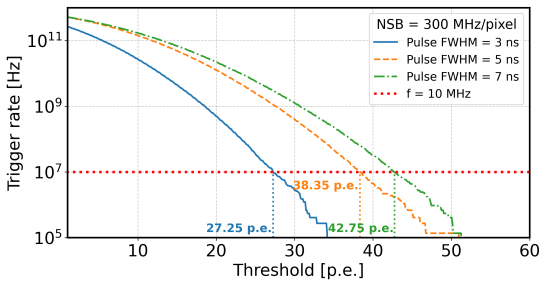
- A camera front-end could sustain 10 MHz trigger rates with a lower threshold: extending the pulse FWHM from 3 ns to 5 ns would raise the threshold by about 40%.
- Single-photon resolution up to about 30 p.e. lets the trigger detect faint 20 GeV Cherenkov events with a false-positive probability around 0.6% at a half-photoelectron threshold.
- Power of 23 mW per pixel makes a multi-thousand-pixel camera feasible on a 1.2 V supply.
- Post-calibration linearity of about 5% up to 300 p.e. fits the camera-level error budget that assigns the front-end a 5% share of the 8% pixel-response requirement.
- The output stage drives both single-ended and pseudo-differential 50 Ω loads, so the same chip can feed commercial or custom 1 GHz ADCs without extra components.
Reading between the lines
- If the simulated 1 nF input-capacitance regime holds in hardware, the same active-summation layout could extend to pixel areas beyond 1 cm2 by adding more sub-sections, since the noise penalty scales roughly as the square root of the summed capacitance.
- The band-pass strategy of keeping only the fast decay component and discarding the slow tail is not SiPM-specific: any large-capacitance photodetector with widely separated time constants could use the same filter topology.
- The measured gain varies linearly with photoelectron number because the amplifier transconductance is quadratic in voltage; an on-chip linearization or per-channel correction would reduce the calibration effort the camera currently needs.
Editorial analysis
A structured set of objections, weighed in public.
Referee Report
Summary. The paper presents FANSIC, a 65 nm CMOS ASIC for the readout of silicon photomultipliers, with an active summation stage to combine signals from four SiPM sections into one pixel channel. The design targets large-area SiPM pixels for Cherenkov telescope cameras. The authors describe the design requirements, circuit architecture, and a characterization performed with a single 3x3 mm2 Hamamatsu S13360 SiPM. The measured output pulse has a FWHM of 2.82 ns, the MPE fit yields a 1-p.e. SNR of 6.98, and the transfer characteristic is calibrated with a sixth-degree polynomial giving residuals within 5%. The paper claims compatibility with input capacitance up to 1 nF and single-photoelectron resolution up to 30 p.e., supported by simulations and extrapolation rather than by measurements in the large-pixel configuration.
Significance. The measured single-channel performance is credible and the characterization methodology (MPE fit, ND-filter transmittance calibration, automated acquisition) is careful and reproducible. If the results hold, the ASIC demonstrates a fast, low-power frontend for small SiPM pixels. However, the central claim of large-area SiPM readout is not supported by the present evidence: the ENP reduction argument in Section 2.2 ignores the noise added by the active summation, the 1 nF input-capacitance regime was never exercised in the laboratory, and the linearity metric is defined relative to a high-order polynomial rather than to a linear response. These issues are load-bearing for the advertised application, so the paper in its current form overstates its conclusions.
major comments (3)
- [Section 2.2, Eq. (2), Section 3.2, Table 4] The ENP reduction argument for pixel splitting is invalid after the active summation. Equation (2) gives ENP≈1 for Ceq=650 pF; splitting the pixel into four sections reduces each section's ENP to about 0.5. However, Section 3.2 sums the four sections into a single output, so the noise of all four sections and their preamplifiers adds in quadrature while the signal from a photoelectron appears in only one section. Using the measured single-section noise values from Table 4 (sigma_e = 0.813 mV·ns, sigma_s = 0.549 mV·ns, gain b = 6.853 mV·ns), the 1-p.e. SNR of the summed output is 6.853/sqrt(4·(0.813^2 + 0.549^2)) ≈ 3.5, which is below the SNR ≥ 5 requirement stated in Section 2.5. The paper does not discuss this noise addition in the summation stage, so the design rationale for large-pixel readout is not established.
- [Section 4, Section 5] The central claim of readout of large SiPMs with input capacitance up to 1 nF and pixel areas around 1 cm² is not validated by the reported measurements. Section 4 characterizes FANSIC only with a single 3x3 mm² S13360 SiPM connected to one input; no measurement is presented with four sections summed, with all four inputs connected, or with an input capacitance near 1 nF. The compatibility with 1 nF is supported only by the analytical estimate in Eq. (2) and by circuit simulations. Consequently, the conclusions in Section 5 that the ASIC achieves 3 ns FWHM and single-photoelectron resolution up to 30 p.e. for the target large-pixel application are extrapolations, not demonstrated experimental results.
- [Section 4.2, Fig. 19] The claim of 'post-calibration non-linearity around 5%' is established by fitting a sixth-degree polynomial to the measured transfer function and reporting the residuals relative to that polynomial. This metric measures the goodness of fit of a flexible calibration curve, not the linearity of the detector response. A sixth-order polynomial can absorb arbitrary nonlinearity, so residuals within 5% are not evidence that the frontend meets the 5% linearity requirement of Section 2.7. The paper itself reports a quadratic dependence of pulse area on photoelectron number at low intensities; without defining a linear-calibration procedure (e.g., a single gain factor), the linearity claim is misleading.
minor comments (5)
- [Abstract and Table 2] The abstract states a pulse duration of 3 ns, while Table 2 lists a measured FWHM of 2.82 ns; the minor discrepancy should be reconciled or explained.
- [Section 2.2] The ENP discussion should explicitly state whether the quoted value is the per-section ENP before summation; the current text leaves this ambiguous.
- [Section 2.5, Eq. (4)] Equation (4) appears to have an incorrect integrand: the Gaussian tail probability should contain exp(-x²/(2σ²)), not exp(-x²/σ²). The resulting 0.62% is consistent with 2.5σ, so the numerical value is correct, but the expression as written is not.
- [Section 4, Fig. 16] The claim of 'FWHM of 3 ns across a dynamic range of 1-250 p.e.' would be better supported by a dedicated plot of FWHM versus photoelectron number; the current figure combines several quantities and the text description is qualitative.
- [References] References [11] and [20] appear to be the same publication (Aguilar et al., NIM A 830, 2016) and should be merged or cross-referenced consistently.
Circularity Check
No significant circularity: FANSIC's headline metrics come from independent measurements and circuit simulations, not from the design inputs.
full rationale
No load-bearing circular step is exhibited. The paper's central measured results (3 ns FWHM, SNR 6.98 for 1 p.e., ~5% post-calibration nonlinearity) are extracted from laboratory data acquired with an external Hamamatsu S13360 SiPM and a calibrated optical chain, or from standalone circuit simulations; they are not obtained by assuming the conclusions. The ENP splitting estimate (Eqs. 1-2) is an analytic noise calculation used to motivate the four-section architecture, not a quantity later reported as a measured prediction. The MPE fit (Table 4) yields gain and noise parameters, and SNR is then computed from the defining relation Eq. 10; this is standard device characterization rather than a fitted input disguised as a prediction. The sixth-degree polynomial calibration and its residual are a calibration figure of merit, not a derivation of linearity from first principles. Self-citations [1], [4], and [22] supply application context, shower-simulation inputs, and the generalized-Poisson fitting method; none is used as a uniqueness theorem or as the sole justification of the central measured claims. The large-pixel/1 nF compatibility assertion is an extrapolation from a 3x3 mm2 measurement, and the active-summation quadrature-noise budget is a validation concern (the skeptic's SNR~3.5 estimate), but these are correctness risks, not circular reductions by the paper's own equations.
Assumptions & free parameters
free parameters (5)
- SiPM model inputs (Ceq, G, T) =
Ceq=650 pF, G=1e4, T=290 K
- MPE fit coefficients a, b (Eq. 9) =
a=0.0876, b=6.8534 mV ns
- Calibration polynomial coefficients (Fig. 19) =
x0 through x5 (six coefficients)
- Operating configuration control words (Table 3) =
preamp=16, sum=31, cap1=4, buf=8, cap2=8, dac=0
- Integration window =
6 ns
assumptions (5)
- domain assumption SiPM electrical model of Corsi, Marano, and Acerbi (Eqs. 1-3)
- domain assumption Poisson model for NSB arrivals with negligible dead time (Eqs. 7-8)
- standard math Generalized Poisson MPE fit from ref [22] is valid
- ad hoc to paper The 3x3 mm2 measurement transfers to the large segmented pixel
- ad hoc to paper Post-calibration linearity defined against a sixth-order polynomial
Cite this review
Pith. "Pith review of FANSIC: a Fast ANalog SiPM Integrated Circuit for the readout of large silicon photomultipliers." pith.science (2026). https://pith.science/paper/RM25CGY6
@misc{pith2026241109673,
  author       = {Pith},
  title        = {Pith review of: FANSIC: a Fast ANalog SiPM Integrated Circuit for the readout of large silicon photomultipliers},
  year         = {2026},
  howpublished = {\url{https://pith.science/paper/RM25CGY6}},
  note         = {Machine review of arXiv:2411.09673}
}
read the original abstract
Silicon photo-multipliers (SiPM) have been replacing traditional photomultiplier tubes in most light sensing applications. However, when large detection surface coverage is needed, photomultipliers (PMTs) are still the preferred choice. The main reasons are the sensor thermal noise and the duration of the fast component of its signal, both increasing with the sensor surface. In this work we propose an application specific integrated circuit (ASIC), called Fast ANalog SiPM Integrated Circuit (FANSIC), for the readout of large SiPMs addressing these limitations. The ASIC has an active summation stage, which allows to divide a large detection surface into smaller ones offering faster response both in single ended and differential outputs. The high input bandwidth allows to reach full-width-half-maximum (FWHM) signals or the order of 3--5 ns which limits the impact of internal and external uncorrelated noise. The results of the first implementation of FANSIC, designed in CMOS 65 nm technology, is described in this paper.
Figures


Figures from the paper (17 more)


Reference graph
Works this paper leans on
-
[1]
M. Heller, et al., The next generation cameras for the Large-Sized Tele- scopes of the Cherenkov Telescope Array Observatory, PoS ICRC2023 (2023) 740. doi: 10.22323/1.444.0740
-
[2]
J. Aguilar, et al., The front-end electronics and slow control of large area SiPM for the SST-1M camera developed for the CTA experiment, Nucl. Instrum. Meth. A 830 (2016) 219 – 232. URL: http://www. sciencedirect.com/science/article/pii/S0168900216304788. doi:https://doi.org/10.1016/j.nima.2016.05.086
-
[3]
C. Alispach, et al., The SST-1M imaging atmospheric Cherenkov tele- scope for gamma-ray astrophysics, JCAP 02 (2025) 047. doi: 10.1088/ 1475-7516/2025/02/047. arXiv:2409.11310
arXiv 2025
-
[4]
M. Heller, et al., An innovative silicon photomultiplier digitiz- ing camera for gamma-ray astronomy, The European Physical Journal C 77 (2017) 47. URL: https://doi.org/10.1140/epjc/ s10052-017-4609-z . doi:10.1140/epjc/s10052-017-4609-z
doi:10.1140/epjc/ 2017
-
[5]
The MiniBooNE Experiment : An Overview
H. Ray, The miniboone experiment : An overview, 2007. URL: https: //arxiv.org/abs/hep-ex/0701040. arXiv:hep-ex/0701040
work page Pith review arXiv 2007
-
[6]
R. Okubo, I. Belle, Mcp-pmt quantum efficiency monitoring and opera- tion status of the top counter at the belle ii experiment, Nuclear Instru- ments and Methods in Physics Research Section A: Accelerators, Spec- trometers, Detectors and Associated Equipment 1056 (2023) 168627
work page 2023
-
[7]
Akindele, et al., Acceptance tests of hamamatsu r7081 photomultiplier tubes, Journal of Instrumentation 18 (2023) P08015
work page 2023
-
[8]
Allekotte, et al., The surface detector system of the pierre auger obser- vatory, Nuclear Instruments and Methods in Physics Research Section A: Accelerators, Spectrometers, Detectors and Associated Equipment 586 (2008) 409–420
work page 2008
Show all 22 references
-
[9]
Anderhub, et al., Design and operation of F ACT - the first G- APD Cherenkov telescope, Journal of Instrumentation 8 (2013) 6008P
H. Anderhub, et al., Design and operation of F ACT - the first G- APD Cherenkov telescope, Journal of Instrumentation 8 (2013) 6008P. doi:10.1088/1748-0221/8/06/P06008. arXiv:1304.1710. 31
2013 arXiv
-
[10]
D. Depaoli, et al., Development of a sipm pixel prototype for the large-sized telescope of the cherenkov telescope array, Nu- clear Instruments and Methods in Physics Research Section A: Ac- celerators, Spectrometers, Detectors and Associated Equipment 1055 (2023) 168521. URL:...
2023
-
[11]
A. Hahn, et al., Direct comparison of sipm and pmt sensor per- formances in a large-size imaging air cherenkov telescope, Nu- clear Instruments and Methods in Physics Research Section A: Ac- celerators, Spectrometers, Detectors and Associated Equipment 1064 (2024) 169350. URL:...
2024
-
[12]
Angelis, et al., Characterisation of the music asic for large-area silicon photomultipliers for gamma-ray astronomy, Journal of Instrumentation 18 (2023) P01037
D. Angelis, et al., Characterisation of the music asic for large-area silicon photomultipliers for gamma-ray astronomy, Journal of Instrumentation 18 (2023) P01037. URL: https://dx.doi.org/10.1088/1748-0221/ 18/01/P01037. doi:10.1088/1748-0221/18/01/P01037
2023 doi
-
[13]
C. Arcaro, et al., Studies on a silicon-photomultiplier-based camera for imaging atmospheric cherenkov telescopes, Nuclear Instruments and Methods in Physics Research Section A: Ac- celerators, Spectrometers, Detectors and Associated Equipment 876 (2017) 26–30. URL: https://ww...
2017 doi
-
[14]
L. D. Medina Miranda, Characterization of Photosensitive Devices and Design of an Innovative Large-Sized Gamma-ray Telescope Camera, Ph.D. thesis, University of Geneva, 2023. doi: 10.13097/ archive-ouverte/unige:167866
2023
-
[15]
G´ omez, et al., MUSIC: An 8 channel readout ASIC for SiPM arrays, in: F
S. G´ omez, et al., MUSIC: An 8 channel readout ASIC for SiPM arrays, in: F. Berghmans, A. G. Mignani (Eds.), Optical Sensing and Detec- tion IV, volume 9899, International Society for Optics and Photonics, SPIE, 2016, p. 98990G. URL: https://doi.org/10.1117/12.2231095. doi:10...
2016 doi
-
[16]
Corsi, et al., Modelling a silicon photomultiplier (sipm) as a signal source for optimum front-end design, Nuclear Instruments and Methods in Physics Research Section A: Accelerators, Spectrometers, Detectors and Associated Equipment 572 (2007) 416–418
2007
-
[17]
Marano, et al., Silicon photomultipliers electrical model extensive ana- lytical analysis, IEEE Transactions on Nuclear Science 61 (2013) 23–34
2013
-
[18]
Marano, et al., Accurate analytical single-photoelectron response of silicon photomultipliers, IEEE Sensors Journal 14 (2014) 2749–2754
2014
-
[19]
Acerbi, et al., Understanding and simulating sipms, Nuclear Instruments and Methods in Physics Research Section A: Accelerators, Spectrome- ters, Detectors and Associated Equipment 926 (2019) 16–35
2019
-
[20]
J. A. Aguilar, et al., The front-end electronics and slow control of large area SiPM for the SST-1M camera developed for the CTA experiment, Nucl. Instrum. Meth. A830 (2016) 219–232. doi:10.1016/j.nima.2016. 05.086
2016 doi
-
[21]
Aleksi´ c, et al., Measurement of the crab nebula spectrum over three decades in energy with the magic telescopes, Journal of High Energy Astrophysics 5-6 (2015) 30–38
J. Aleksi´ c, et al., Measurement of the crab nebula spectrum over three decades in energy with the magic telescopes, Journal of High Energy Astrophysics 5-6 (2015) 30–38. URL: https://www. sciencedirect.com/science/article/pii/S2214404815000038. doi:https://doi.org/10.1016/j....
2015 doi
-
[22]
Alispach, et al., Large scale characterization and calibration strategy of a SiPM-based camera for gamma-ray astronomy, JINST 15 (2020) P11010
C. Alispach, et al., Large scale characterization and calibration strategy of a SiPM-based camera for gamma-ray astronomy, JINST 15 (2020) P11010. doi:10.1088/1748-0221/15/11/P11010. arXiv:2008.04716. 33
2020 arXiv
Reviewed August 12, 2026 · model on record in the stance chip above.
Discussion (0). Continue with ORCID to comment.