REVIEW 3 major objections 5 minor 1 cited by
Direct imprinting of arbitrary spin textures using programmable structured light in a semiconductor two-dimensional electron gas
T0 review · 3 major / 5 minor · reviewed 2026-08-12 · deepseek-v4-flash
Pith's one-line read Structured light imprints programmable spin helices in GaAs
desk verdict Solid experimental demonstration of programmable spin-helix imprinting with tunable wave number, but the 'arbitrary spin textures' claim outruns the single-mode data. read the letter →
The pith
A machine-rendered reading of the paper's core claim, the machinery that carries it, and where it could break.
The reading
What carries the argument
The central object is a reflective liquid-crystal spatial light modulator used as a programmable phase plate. It accepts $D$-polarized (45-degree linear) pump light and advances the phase of one component by $\delta = 0$ to $2\pi$, producing the polarization cycle $D \to R \to A \to L$ in space; after $1/75$ demagnification onto the sample, a phase advance of $2\pi$ every $N$ SLM pixels becomes a polarization grating with wavelength in the range $5.24$ to $62.8~\mu\mathrm{m}$. The load-bearing transfer step is the optical selection rule, which assigns up-spin to right-circular polarization and down-spin to left-circular polarization, so the spatial pattern of circular polarization becomes a spatial pattern of out-of-plane spin. The signature is measured by pump-probe Kerr rotation, and the analysis extracts $q_0$ from a two-dimensional Fourier transform of the spin map.
What would settle it
Imprint a deliberately non-sinusoidal polarization pattern, such as a step function or a narrow stripe, onto the same quantum well; if the measured Kerr map at $t=0$ does not reproduce the sharp edge within the resolution set by the probe spot and Fourier bandwidth, then the polarization-to-spin transfer is filtered rather than direct, and the arbitrary-texture claim fails.
Extended reading notes
Core claim
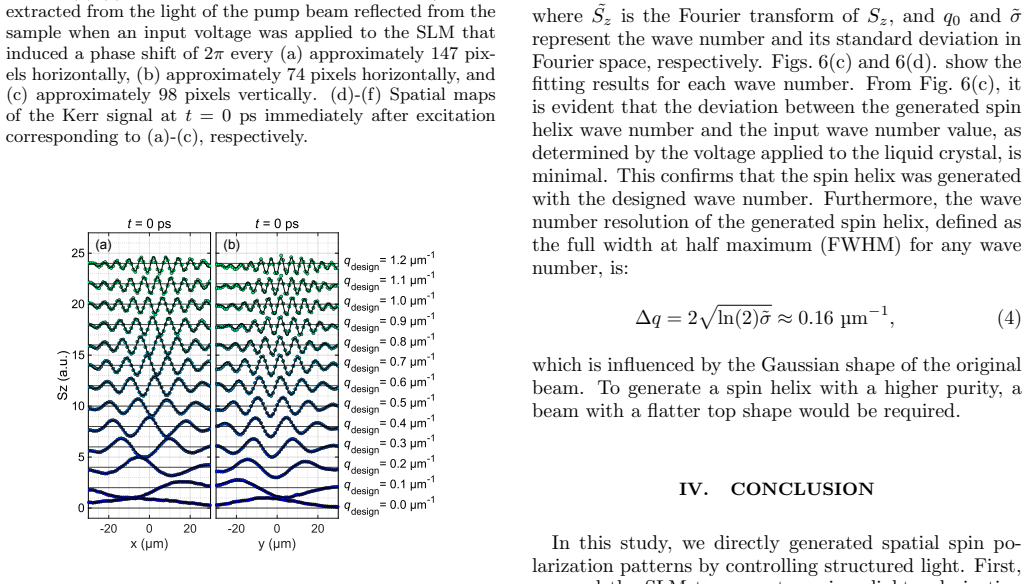
On the paper's own terms, the discovery is that the optical selection rule in a GaAs/AlGaAs quantum well transfers a spatially structured light polarization pattern into a matching spatial spin pattern, so a helix with designed wave number $q_{\mathrm{design}}$ appears in the Kerr-rotation map at $t=0$. The authors verify this by imaging the pump's circular-polarization component $S_3/S_0$ on the sample, generating spin helices along $x\parallel[\bar{1}10]$ and $y\parallel[110]$, and fitting the two-dimensional Fourier transform of the spin map to a Gaussian envelope combined with $\cos(q_0 r + \phi)$. The fitted central wave number tracks the designed value over $q_{\mathrm{design}} = 0$ to $1.2~\mu\mathrm{m}^{-1}$, with an instrument-limited wave-number resolution of approximately $0.16~\mu\mathrm{m}^{-1}$.
Load-bearing premise
The load-bearing premise is that the polarization pattern produced by the spatial light modulator survives demagnification and focusing onto the sample and maps one-to-one onto the electron spin pattern seen by the Kerr measurement at $t=0$, without distortion from diffraction, depolarization, or the finite probe spot.
Editorial extensions
If this is right
- Spin helix wavelength becomes a software parameter: changing the SLM pixel period changes the helix period on the sample without fabricating a new grating.
- The same optical path can pattern spins in two orthogonal directions, $x$ and $y$, by rotating the phase-gradient direction on the SLM.
- Wave numbers from 0 to 1.2 inverse micrometres, corresponding to periods from infinity to about 5 micrometres, are reachable, covering a wider range than gate tuning of spin-orbit coupling alone.
- The approach should transfer to any material with strong polarization-to-spin coupling, such as other III-V quantum wells, halide perovskites, transition-metal dichalcogenides, and magnetic thin films.
- Replacing the Gaussian pump beam with a flatter-top beam would sharpen the wave-number peak beyond the current resolution of approximately $0.16~\mu\mathrm{m}^{-1}$.
Reading between the lines
- The paper demonstrates sinusoidal helices, not arbitrary textures; a true test of the title's promise would be imprinting a non-sinusoidal pattern, such as a spin domain wall or a checkerboard, and showing the measured map follows the designed pattern beyond its Fourier peak.
- The claimed one-to-one polarization-to-spin transfer is inferred from matching wave numbers; a direct pixel-by-pixel correlation between the pump's $S_3/S_0$ map and the Kerr map would separate genuine imprinting fidelity from envelope and phase coincidences.
- If the method is as general as claimed, the same SLM path could write vector-beam-like spin textures and holographic spin patterns, effectively using structured light as a reconfigurable mask for spin-based logic; the paper mentions this direction but does not demonstrate it.
Editorial analysis
A structured set of objections, weighed in public.
Referee Report
Summary. The paper reports a method for imprinting spin textures in a GaAs/AlGaAs two-dimensional electron gas by spatially modulating the polarization of a pump beam with a spatial light modulator (SLM). Using pump-probe Kerr rotation microscopy, the authors show that a periodic polarization pattern produces a periodic spin pattern (spin helix) whose wave number can be designed from 0 to 1.2 µm^-1 in both horizontal and vertical directions. They verify the SLM's polarization control via Stokes parameter measurements and compare the measured spin maps with the designed polarization patterns.
Significance. If fully validated, the method offers a programmable, mask-free alternative to transient spin grating spectroscopy and conventional spatial- and time-resolved Kerr rotation microscopy, with potential applicability to other spin-photon-coupled materials. The demonstration of tunable spin helix wave numbers over a wide range is a useful and credible experimental advance. The paper also provides a clear step-by-step characterization of the SLM-based system. However, the stronger claim in the title and abstract of 'arbitrary spin textures' is not supported by the presented data, which only demonstrate single-mode sinusoidal patterns, and the quantitative verification of spatial fidelity is incomplete.
major comments (3)
- [Title/Abstract and Section IV (Conclusion)] The claim of 'arbitrary spin textures' is not supported by the experiments shown. All demonstrated patterns are single-mode sinusoidal spin helices, and the quantitative validation in Section III fits each Kerr map to Eq. (2), a Gaussian-envelope cosine, extracting only the fundamental wave number q0. No experiment demonstrates a texture with multiple wave numbers, sharp features, or a non-sinusoidal pattern, which is what 'arbitrary' would require. This is a load-bearing overclaim for the paper's central novelty. I recommend either softening the title/abstract to 'programmable spin helix generation' or adding a demonstration of a more complex texture with a quantitative fidelity metric.
- [Section III, Fig. 6(c)] The central quantitative claim that the generated wave number matches the design is presented without error bars or a numerical deviation measure. The text states that the deviation is 'minimal' but provides no quantitative bound. Please report the fitted q0 values with uncertainties from the nonlinear fits, include the ideal line q0 = qdesign, and give a goodness-of-fit statistic (or a table of fitted versus designed values). This is necessary for the reader to assess the claimed accuracy of the wave number control.
- [Section II.D and Section III] The one-to-one correspondence between the imprinted polarization pattern and the measured spin map is only verified by visual comparison of Fig. 3 and Fig. 4. There is no quantitative comparison (e.g., normalized cross-correlation, residual map, or structure-similarity index) between the Stokes-parameter image S3/S0 and the Kerr map, and no spatial registration procedure is described. Given that the probe spot has σ < 1.3 µm and the pump passes through an objective lens that may introduce aberrations or polarization changes, a quantitative fidelity check is needed to support the claim that the spin distribution is a faithful copy of the designed polarization pattern.
minor comments (5)
- [Section II.C and Table I] The text says the pattern in Fig. 3(d) was created by shifting the phase by 2π every 96 pixels, while Table I lists 98.17 pixels for q = 0.6 µm^-1, which is the corresponding design value. Please make these numbers consistent or explain the rounding.
- [Eq. (2)] The variable r in Eq. (2) is not defined in the two-dimensional context. Please specify whether the fit is performed along a one-dimensional line profile or provide the two-dimensional form with wave vector q.
- [Figures 4 and 6] Clarify that the color scale labeled 'Sz (a.u.)' refers to the out-of-plane electron spin component inferred from the measured Kerr rotation angle, and state the conversion or normalization used.
- [Section III, Eq. (4)] The value of σ̃ used to compute Δq in Eq. (4) is not reported. Please give the fitted value of σ̃ and its uncertainty so the reader can assess the spectral width of the generated spin helix.
- [Introduction and Abstract] The term 'spin helix' is used for the imprinted periodic spin pattern, but this may be confused with the persistent spin helix state, which arises from spin-orbit coupling. Since the imprinted pattern is a static spin polarization grating created by the optical selection rule, consider defining 'spin helix' explicitly at first use.
Circularity Check
No significant circularity: the spin-helix wave number is measured independently and compared with the design input, with no fitted parameter reused as a prediction.
full rationale
This is an experimental demonstration rather than a derivation. The input wave number qdesign is set from the SLM pixel period and the demagnification listed in Table I, while the measured Kerr maps are fit to Eq. (2) to extract a central wave number q0; the two quantities are then compared in Fig. 6(c). The fitted parameters are not fed back into the input, so the comparison is not forced by construction. Eq. (3) is the ordinary Fourier transform of Eq. (2), not an independent claim. The optical selection rule is cited to standard prior work [57] and is separately checked in Fig. 2(c) by comparing R/A/L polarization excitations. The only self-citations ([18], [29]) are contextual references to prior imaging and persistent-spin-helix work and are not load-bearing premises for the measured matching. The manuscript itself notes that the Gaussian envelope limits the purity of the spin helix, acknowledging a limitation rather than hiding it. The title's 'arbitrary spin textures' phrasing is broader than the demonstrated single-cosine fits, but that is a validation-scope concern, not a circularity.
Assumptions & free parameters
free parameters (3)
- Spin helix wave number q0 =
0 to 1.2 inverse micrometers (see Fig. 6(c))
- Envelope parameters A, r0, sigma, phi =
Not tabulated
- Wave number spread sigma_tilde =
Delta q about 0.16 inverse micrometers (FWHM)
assumptions (4)
- domain assumption Optical selection rule: circularly polarized light maps to electron spin polarization in GaAs with one-to-one correspondence
- domain assumption SLM acts as a linear wave plate: phase difference between x and y components is proportional to input voltage
- ad hoc to paper The pump intensity profile and the imprinted spin pattern are Gaussian-envelope cosine distributions
- domain assumption Measured Kerr rotation is proportional to the out-of-plane electron spin component
Cite this review
Pith. "Pith review of Direct imprinting of arbitrary spin textures using programmable structured light in a semiconductor two-dimensional electron gas." pith.science (2026). https://pith.science/paper/LRCTOSO3
@misc{pith2026241110963,
  author       = {Pith},
  title        = {Pith review of: Direct imprinting of arbitrary spin textures using programmable structured light in a semiconductor two-dimensional electron gas},
  year         = {2026},
  howpublished = {\url{https://pith.science/paper/LRCTOSO3}},
  note         = {Machine review of arXiv:2411.10963}
}
read the original abstract
Precise control of spatial spin structures, such as spin helices, is critical for advancing spintronic devices, particularly in non-volatile, low-power information storage and processing. Conventional techniques, including transient spin grating spectroscopy and spatial- and time-resolved Kerr rotation microscopy, are limited by fixed optical grating periods and uniform light polarization, respectively, which constrain the flexibility of spin helix generation. Here, we introduce a novel approach utilizing structured light to directly imprint spatial spin structures in a GaAs/AlGaAs quantum well. This method allows for the precise control over the wave number and configuration of the spin helices, overcoming the limitations of previous techniques. Experiments conducted using pump-probe Kerr rotation microscopy combined with a programmable spatial light modulator revealed the efficient and tunable generation of spin helices. This approach is broadly applicable not only to semiconductors but also to magnetic thin films and 2D materials.
Figures


Figures from the paper (2 more)

Forward citations
Cited by 1 Pith paper
-
Persistent spin grids with spin-orbit coupled 2D electron gas
Spin relaxation in a 2D electron gas can be suppressed by confining it to a grid of narrow channels, with a Z2 topological classification of the resulting persistent spin grids.
Reference graph
Works this paper leans on
-
[1]
J. Schliemann and D. Loss, Anisotropic transport in a two-dimensional electron gas in the presence of spin-orbit coupling, Phys. Rev. B 68, 165311 (2003)
work page 2003
-
[2]
B. A. Bernevig, J. Orenstein, and S.-C. Zhang, Exact SU(2) symmetry and persistent spin helix in a spin-orbit coupled system, Phys. Rev. Lett. 97, 236601 (2006)
work page 2006
-
[3]
J. D. Koralek, C. P. Weber, J. Orenstein, B. A. Bernevig, S.-C. Zhang, S. Mack, and D. D. Awschalom, Emergence of the persistent spin helix in semiconductor quantum wells, Nature 458, 610 (2009)
work page 2009
- [4]
-
[5]
M. P. Walser, C. Reichl, W. Wegscheider, and G. Salis, Direct mapping of the formation of a persistent spin he- lix, Nat. Phys. 8, 757 (2012)
work page 2012
- [6]
-
[7]
M. Kohda and G. Salis, Physics and application of persis- tent spin helix state in semiconductor heterostructures, Semicond. Sci. Technol. 32, 073002 (2017)
work page 2017
-
[8]
E. I. Rashba, Properties semiconductors extremum loop
Show all 58 references
-
[9]
cyclotron combinational resonance magnetic field per- pendicular plane loop, Sov. Phys. Solid State 2, 1109 (1960)
1960
-
[10]
Y. A. Bychkov and E. I. Rashba, Oscillatory effects and the magnetic susceptibility of carriers in inversion layers, J. Phys. 17, 6039 (1984)
1984
-
[11]
Dresselhaus, Spin-orbit coupling effects in zinc blende structures, Phys
G. Dresselhaus, Spin-orbit coupling effects in zinc blende structures, Phys. Rev. 100, 580 (1955)
1955
-
[12]
Chuang, S.-C
P. Chuang, S.-C. Ho, L. W. Smith, F. Sfigakis, M. Pep- per, C.-H. Chen, J.-C. Fan, J. P. Griffiths, I. Farrer, H. E. Beere, G. A. C. Jones, D. A. Ritchie, and T.-M. Chen, All-electric all-semiconductor spin field-effect transistors, Nat. Nanotechnol. 10, 35 (2015)
2015
-
[13]
Dettwiler, J
F. Dettwiler, J. Fu, S. Mack, P. J. Weigele, J. Car- los Egues, D. D. Awschalom, and D. M. Zumb¨ uhl, Stretchable persistent spin helices in GaAs quantum wells, Phys. Rev. X 7, 031010 (2017)
2017
-
[14]
Kohda, T
M. Kohda, T. Seki, Y. Yuminaka, T. Uemura, K. Kikuchi, and G. Salis, Perspective on spin-based wave-parallel computing, Appl. Phys. Lett. 123, 190502 (2023)
2023
-
[15]
C. P. Weber, J. Orenstein, B. A. Bernevig, S.-C. Zhang, J. Stephens, and D. D. Awschalom, Nondiffusive spin dynamics in a two-dimensional electron gas, Phys. Rev. Lett. 98, 076604 (2007)
2007
-
[16]
L. Yang, J. D. Koralek, J. Orenstein, D. R. Tibbetts, J. L. Reno, and M. P. Lilly, Measurement of electron- hole friction in an n-doped GaAs/AlGaAs quantum well using optical transient grating spectroscopy, Phys. Rev. Lett. 106, 247401 (2011)
2011
-
[17]
L. Yang, J. D. Koralek, J. Orenstein, D. R. Tibbetts, J. L. Reno, and M. P. Lilly, Doppler velocimetry of spin prop- agation in a two-dimensional electron gas, Nat. Phys. 8, 7 153 (2012)
2012
-
[18]
L. Yang, J. D. Koralek, J. Orenstein, D. R. Tibbetts, J. L. Reno, and M. P. Lilly, Coherent propagation of spin helices in a quantum-well confined electron gas, Phys. Rev. Lett. 109, 246603 (2012)
2012
-
[19]
Ishihara, Y
J. Ishihara, Y. Ohno, and H. Ohno, Direct imag- ing of gate-controlled persistent spin helix state in a modulation-doped GaAs/AlGaAs quantum well, Appl. Phys. Express 7, 013001 (2013)
2013
-
[20]
Salis, M
G. Salis, M. P. Walser, P. Altmann, C. Reichl, and W. Wegscheider, Dynamics of a localized spin excitation close to the spin-helix regime, Phys. Rev. B 89, 045304 (2014)
2014
-
[21]
Ishihara, Y
J. Ishihara, Y. Ohno, and H. Ohno, Direct map- ping of photoexcited local spins in a modulation-doped GaAs/AlGaAs wires, Jpn. J. Appl. Phys. 53, 04EM04 (2014)
2014
-
[22]
Altmann, M
P. Altmann, M. P. Walser, C. Reichl, W. Wegscheider, and G. Salis, Suppressed decay of a laterally confined persistent spin helix, Phys. Rev. B 90, 201306 (2014)
2014
-
[23]
Y. S. Chen, S. F¨ alt, W. Wegscheider, and G. Salis, Uni- directional spin-orbit interaction and spin-helix state in a (110)-oriented GaAs/(al,ga)as quantum well, Phys. Rev. B 90, 121304 (2014)
2014
-
[24]
Altmann, F
P. Altmann, F. G. G. Hernandez, G. J. Ferreira, M. Ko- hda, C. Reichl, W. Wegscheider, and G. Salis, Current- controlled spin precession of quasistationary electrons in a cubic spin-orbit field, Phys. Rev. Lett. 116, 196802 (2016)
2016
-
[25]
Kunihashi, H
Y. Kunihashi, H. Sanada, H. Gotoh, K. Onomitsu, M. Kohda, J. Nitta, and T. Sogawa, Drift transport of he- lical spin coherence with tailored spin-orbit interactions, Nat. Commun. 7, 10722 (2016)
2016
-
[26]
Passmann, S
F. Passmann, S. Anghel, T. Tischler, A. V. Poshakinskiy, S. A. Tarasenko, G. Karczewski, T. Wojtowicz, A. D. Bristow, and M. Betz, Persistent spin helix manipulation by optical doping of a CdTe quantum well, Phys. Rev. B 97, 201413 (2018)
2018
-
[27]
Anghel, F
S. Anghel, F. Passmann, K. J. Schiller, J. N. Moore, G. Yusa, T. Mano, T. Noda, M. Betz, and A. D. Bristow, Spin-locked transport in a two-dimensional electron gas, Phys. Rev. B. 101, 155414 (2020)
2020
-
[28]
Anghel, A
S. Anghel, A. V. Poshakinskiy, K. Schiller, F. Pass- mann, C. Ruppert, S. A. Tarasenko, G. Yusa, T. Mano, T. Noda, and M. Betz, Anisotropic expansion of drifting spin helices in GaAs quantum wells, Phys. Rev. B. 103, 035429 (2021)
2021
-
[29]
Ishihara, T
J. Ishihara, T. Suzuki, G. Kitazawa, T. Mori, Y. Ohno, and K. Miyajima, Spatiotemporal spin dynamics of two- dimensional electron gas with ballistic motion in persis- tent spin helix state, Phys. Rev. B. 105, 144412 (2022)
2022
-
[30]
Ishihara, T
J. Ishihara, T. Mori, T. Suzuki, S. Sato, K. Morita, M. Kohda, Y. Ohno, and K. Miyajima, Imprinting spatial helicity structure of vector vortex beam on spin texture in semiconductors, Phys. Rev. Lett. 130, 126701 (2023)
2023
-
[31]
Kawaguchi, T
K. Kawaguchi, T. Fukasawa, I. Takazawa, H. Shida, Y. Saito, D. Iizasa, T. Saito, T. Kitada, Y. Ishitani, M. Kohda, and K. Morita, Transient diffusive spin dy- namics in intrinsic InGaAs/InAlAs multiple quantum wells, Appl. Phys. Lett. 115, 172406 (2019)
2019
-
[32]
Arikawa, Y
A. Arikawa, Y. Saito, K. Nakanishi, S. Sato, K. Sugaya, N. Yokota, M. Kohda, and K. Morita, D’yakonov–Perel and Elliot–Yafet spin relaxation rates in InGaAs/InAlAs multiple quantum wells at room temperature, Appl. Phys. Express 15, 043001 (2022)
2022
-
[33]
J. W. McIver, D. Hsieh, H. Steinberg, P. Jarillo-Herrero, and N. Gedik, Control over topological insulator pho- tocurrents with light polarization, Nat. Nanotechnol. 7, 96 (2011)
2011
-
[34]
Giovanni, H
D. Giovanni, H. Ma, J. Chua, M. Gr¨ atzel, R. Ramesh, S. Mhaisalkar, N. Mathews, and T. C. Sum, Highly spin- polarized carrier dynamics and ultralarge photoinduced magnetization in CH3NH3PbI3 perovskite thin films, Nano Lett. 15, 1553 (2015)
2015
-
[35]
Boschini, M
F. Boschini, M. Mansurova, G. Mussler, J. Kampmeier, D. Gr¨ utzmacher, L. Braun, F. Katmis, J. S. Mood- era, C. Dallera, E. Carpene, C. Franz, M. Czerner, C. Heiliger, T. Kampfrath, and M. M¨ unzenberg, Coher- ent ultrafast spin-dynamics probed in three dimensional topological...
2015
-
[36]
Y. Q. Huang, Y. X. Song, S. M. Wang, I. A. Buyanova, and W. M. Chen, Spin injection and helicity control of surface spin photocurrent in a three dimensional topo- logical insulator, Nat. Commun. 8, 15401 (2017)
2017
-
[37]
Odenthal, W
P. Odenthal, W. Talmadge, N. Gundlach, R. Wang, C. Zhang, D. Sun, Z.-G. Yu, Z. Valy Vardeny, and Y. S. Li, Spin-polarized exciton quantum beating in hybrid or- ganic–inorganic perovskites, Nat. Phys. 13, 894 (2017)
2017
-
[38]
Yumoto, F
G. Yumoto, F. Sekiguchi, R. Hashimoto, T. Nakamura, A. Wakamiya, and Y. Kanemitsu, Rapidly expanding spin-polarized exciton halo in a two-dimensional halide perovskite at room temperature, Sci. Adv. 8, eabp8135 (2022)
2022
-
[39]
Anghel, A
S. Anghel, A. V. Poshakinskiy, D. R. Yakovlev, E. Kirstein, N. E. Kopteva, O. Hordiichuk, M. V. Ko- valenko, M. Bayer, and M. Betz, Fast diffusion of spin polarized excitons in organic–inorganic lead halide per- ovskites, ACS Photonics 10, 4169 (2023)
2023
-
[40]
C. R. Zhu, K. Zhang, M. Glazov, B. Urbaszek, T. Amand, Z. W. Ji, B. L. Liu, and X. Marie, Exciton valley dynam- ics probed by kerr rotation in WSe2 monolayers, Phys. Rev. B Condens. Matter Mater. Phys. 90, 161302 (2014)
2014
-
[41]
L. Yang, W. Chen, K. M. McCreary, B. T. Jonker, J. Lou, and S. A. Crooker, Spin coherence and dephasing of lo- calized electrons in monolayer MoS2, Nano Lett.15, 8250 (2015)
2015
-
[42]
L. Yang, N. A. Sinitsyn, W. Chen, J. Yuan, J. Zhang, J. Lou, and S. A. Crooker, Long-lived nanosecond spin relaxation and spin coherence of electrons in monolayer MoS2 and WS2, Nat. Phys. 11, 830 (2015)
2015
-
[43]
Plechinger, P
G. Plechinger, P. Nagler, A. Arora, R. Schmidt, A. Chernikov, A. G. Del ´Aguila, P. C. M. Christianen, R. Bratschitsch, C. Sch¨ uller, and T. Korn, Trion fine structure and coupled spin-valley dynamics in monolayer tungsten disulfide, Nat. Commun. 7, 12715 (2016)
2016
-
[44]
Huang, T
J. Huang, T. B. Hoang, T. Ming, J. Kong, and M. H. Mikkelsen, Temporal and spatial valley dynamics in two- dimensional semiconductors probed via kerr rotation, Phys. Rev. B. 95, 075428 (2017)
2017
-
[45]
E. J. McCormick, M. J. Newburger, Y. K. Luo, K. M. McCreary, S. Singh, I. B. Martin, E. J. Cichewicz, Jr, B. T. Jonker, and R. K. Kawakami, Imaging spin dy- namics in monolayer WS 2 by time-resolved kerr rotation microscopy, 2d Mater. 5, 011010 (2017)
2017
-
[46]
Huang, G
B. Huang, G. Clark, E. Navarro-Moratalla, D. R. Klein, R. Cheng, K. L. Seyler, D. Zhong, E. Schmidgall, M. A. McGuire, D. H. Cobden, W. Yao, D. Xiao, P. Jarillo- 8 Herrero, and X. Xu, Layer-dependent ferromagnetism in a van der waals crystal down to the monolayer limit, Nature...
2017
-
[47]
Huang, G
B. Huang, G. Clark, D. R. Klein, D. MacNeill, E. Navarro-Moratalla, K. L. Seyler, N. Wilson, M. A. McGuire, D. H. Cobden, D. Xiao, W. Yao, P. Jarillo- Herrero, and X. Xu, Electrical control of 2D magnetism in bilayer CrI3, Nat. Nanotechnol. 13, 544 (2018)
2018
-
[48]
Cenker, B
J. Cenker, B. Huang, N. Suri, P. Thijssen, A. Miller, T. Song, T. Taniguchi, K. Watanabe, M. A. McGuire, D. Xiao, and X. Xu, Direct observation of two- dimensional magnons in atomically thin CrI3, Nat. Phys. 17, 20 (2021)
2021
-
[49]
Cheng, Z
X. Cheng, Z. Cheng, C. Wang, M. Li, P. Gu, S. Yang, Y. Li, K. Watanabe, T. Taniguchi, W. Ji, and L. Dai, Light helicity detector based on 2D magnetic semicon- ductor CrI3, Nat. Commun. 12, 6874 (2021)
2021
-
[50]
Zhang, T.-F
P. Zhang, T.-F. Chung, Q. Li, S. Wang, Q. Wang, W. L. B. Huey, S. Yang, J. E. Goldberger, J. Yao, and X. Zhang, All-optical switching of magnetization in atomically thin CrI3, Nat. Mater. 21, 1373 (2022)
2022
-
[51]
Lambert, S
C.-H. Lambert, S. Mangin, B. S. D. C. S. Varaprasad, Y. K. Takahashi, M. Hehn, M. Cinchetti, G. Malinowski, K. Hono, Y. Fainman, M. Aeschlimann, and E. E. Fuller- ton, All-optical control of ferromagnetic thin films and nanostructures, Science 345, 1337 (2014)
2014
-
[52]
M. S. El Hadri, M. Hehn, P. Pirro, C.-H. Lambert, G. Malinowski, E. E. Fullerton, and S. Mangin, Domain size criterion for the observation of all-optical helicity- dependent switching in magnetic thin films, Phys. Rev. B 94, 064419 (2016)
2016
-
[53]
Y. K. Takahashi, R. Medapalli, S. Kasai, J. Wang, K. Ish- ioka, S. H. Wee, O. Hellwig, K. Hono, and E. E. Fullerton, Accumulative magnetic switching of ultrahigh-density recording media by circularly polarized light, Phys. Rev. Appl. 6, 054004 (2016)
2016
-
[54]
R. John, M. Berritta, D. Hinzke, C. M¨ uller, T. San- tos, H. Ulrichs, P. Nieves, J. Walowski, R. Mondal, O. Chubykalo-Fesenko, J. McCord, P. M. Oppeneer, U. Nowak, and M. M¨ unzenberg, Magnetisation switching of FePt nanoparticle recording medium by femtosecond laser pulses, ...
2017
-
[55]
Kichin, M
G. Kichin, M. Hehn, J. Gorchon, G. Malinowski, J. Hohlfeld, and S. Mangin, From multiple- to single- pulse all-optical helicity-dependent switching in ferro- magnetic co/pt multilayers, Phys. Rev. Appl. 12, 024019 (2019)
2019
-
[56]
G.-M. Choi, J. H. Oh, D.-K. Lee, S.-W. Lee, K. W. Kim, M. Lim, B.-C. Min, K.-J. Lee, and H.-W. Lee, Op- tical spin-orbit torque in heavy metal-ferromagnet het- erostructures, Nat. Commun. 11, 1482 (2020)
2020
-
[57]
Iihama, K
S. Iihama, K. Ishibashi, and S. Mizukami, Interface- induced field-like optical spin torque in a ferromag- net/heavy metal heterostructure, Nanophotonics 10, 1169 (2021)
2021
-
[58]
A. R. Cameron, P. Riblet, and A. Miller, Spin gratings and the measurement of electron drift mobility in multi- ple quantum well semiconductors, Phys. Rev. Lett. 76, 4793 (1996)
1996
Reviewed August 12, 2026 · model on record in the stance chip above.
Discussion (0). Continue with ORCID to comment.