REVIEW 4 major objections 7 minor 29 references
Space Charge Doping Induced Band Modulation in Mono- and Bi-layer Graphene: a nano-ARPES study
T0 review · 4 major / 7 minor · reviewed 2026-08-10 · deepseek-v4-flash
Pith's one-line read The paper claims that space charge doping of graphene on glass directly shifts the Fermi level by about 500 meV in monolayer and 250 meV in bilayer graphene, observed by nano-ARPES.
desk verdict Plausible but under-supported: the space-charge doping shift in graphene is likely real in direction, but the 500/250 meV numbers rest on an unverified energy reference. read the letter →
The pith
A machine-rendered reading of the paper's core claim, the machinery that carries it, and where it could break.
The reading
What carries the argument
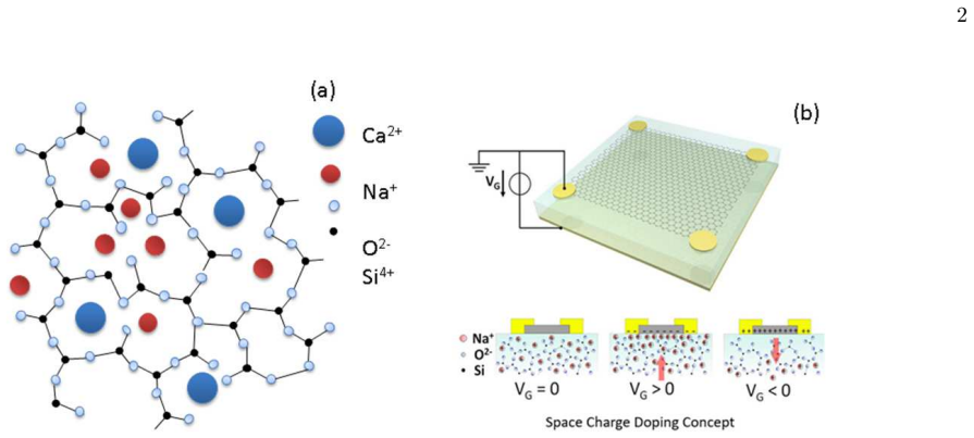
The mechanism is space charge doping in soda-lime glass: heating activates sodium ions, an external voltage piles them up at or depletes them from the glass surface, and cooling quenches the charge distribution so the doping persists. The glass surface then acts as a built-in electrostatic gate for the graphene flake. Nano-ARPES with sub-micron spatial resolution resolves the band structure of individual micron-sized flakes and reads the Fermi-level shift directly from the band position in energy.
What would settle it
Re-measure the undoped graphene flake repeatedly over the same acquisition time with no voltage applied: if the Dirac-point position drifts by hundreds of meV, or if returning to the 'undoped' condition after a doping cycle does not restore the original band position, the reported shifts would not be controlled doping. Alternatively, compare the graphene band position with a simultaneously measured gold Fermi edge; a fixed Fermi edge with a moving graphene band would confirm real doping, while a moving Fermi edge would indicate charging or reference drift.
Extended reading notes
Core claim
The central claim is that space charge doping on soda-lime glass produces a large, reversible, and persistent Fermi-level shift in monolayer and bilayer graphene, and that this shift can be followed directly in momentum-resolved photoemission. On monolayer graphene the observed shift is about 500 meV, on bilayer about 250 meV, with hole or electron doping selected by the sign of the applied voltage. Because the charge distribution in the glass is quenched by cooling, the doped state survives without a maintained gate voltage, which is the distinctive advantage the authors claim over conventional electrostatic gating.
Load-bearing premise
The central claim rests on taking the measured ARPES energy positions as true Fermi-level shifts, but the paper reports no calibration of the energy reference against a known feature or test for sample charging, so a drifting reference would make the 500 meV and 250 meV values artifacts rather than real doping.
Editorial extensions
If this is right
- Monolayer graphene can be p- and n-doped simply by reversing polarity, achieving about 500 meV Fermi-level shift without chemical dopants.
- Bilayer graphene shows about 250 meV shift, indicating the doping effect depends on layer thickness.
- The quenched space charge means the doped state persists after the voltage is removed, allowing measurements and potential devices without a maintained gate.
- The combination of space charge doping and nano-ARPES can be extended to other 2D materials to directly observe band gap transitions and phase transitions as a function of carrier doping.
- Direct visualization of Fermi-level tuning on micron-sized flakes is possible with this approach.
Reading between the lines
- If the shifts are real Fermi-level movements, the linear graphene dispersion lets one convert the 500 meV and 250 meV shifts into carrier densities, providing a quantitative estimate of the space charge accumulated at the glass surface.
- The persistence of doping after voltage removal could enable remanent p-n junctions or spatially patterned doping on glass without keeping contacts powered, a consequence the authors mention only as future device applications.
- A decisive control would be comparing the graphene band position with a simultaneously measured gold Fermi edge or a core level, which would separate true doping from sample charging or energy-reference drift.
- The broad monolayer bands noted in the paper may make the 500 meV monolayer shift harder to pin down than the sharper bilayer value, so the layer-thickness comparison itself could be tested by higher-resolution measurements.
Editorial analysis
A structured set of objections, weighed in public.
Referee Report
Summary. The manuscript reports a combined space charge doping and nano-ARPES study of monolayer and bilayer graphene flakes on soda-lime glass. The authors claim to observe reversible p- and n-type doping that shifts the graphene bands by approximately 500 meV (monolayer) and 250 meV (bilayer) relative to the undoped state, as evidenced by energy distribution curve (EDC) and momentum distribution curve (MDC) comparisons. The paper argues that the space charge doping technique, previously demonstrated by the same group on MoS2, can be applied to graphene and directly visualized with sub-micrometer photoemission.
Significance. If the quantitative claims were rigorously supported, this work would provide a practical demonstration of a contact-free doping scheme for 2D materials and show that nano-ARPES can directly track Fermi level movement on micron-sized flakes. The direct photoemission observation of band shifts, rather than inference from transport, is a strength of the approach, and the extension to a common substrate (glass) is potentially useful. However, the manuscript currently lacks the energy calibration, error analysis, and doping-cycle data necessary to substantiate the headline numbers; the central quantitative claims therefore rest on plausible but unverified reading of the data.
major comments (4)
- [Experimental section, paragraph beginning 'The sample was well grounded'] The assertion that grounding prevents charging is not a calibration. No Fermi edge of a metallic reference, core-level line, or other independent energy reference is reported, so the 500 meV and 250 meV shifts in Fig. 7 could equally arise from contact potential drift, analyzer work function changes, or beam-induced common-mode shifts between acquisitions. The authors should either provide an energy calibration (e.g., a gold Fermi edge measured under identical conditions before and after each doping state) or clearly restrict their claim to relative shifts within a single continuous scan with a demonstrated stable reference.
- [Figs. 4, 6, and 7 (EDC/MDC analysis)] The reported shifts are not quantified with error bars or a fitting procedure. The monolayer bands are explicitly described as broad, and Fig. 4 suggests the EDC edges are gradual; visual determination of a band edge is therefore ambiguous. The authors should specify the criterion used to extract the shift (e.g., linear extrapolation of the leading edge, a fixed intensity threshold, or peak position of the MDC), report the uncertainty on each shift, and show representative fits or overlaid extraction lines on the EDCs.
- [Results paragraph ending 'simply by reversing polarity of external voltage' and Conclusion] The claims that the doping is 'reversible' and that hole and electron doping were achieved 'simply by reversing polarity' are not supported by any shown data. No spectra are presented that demonstrate a return to the undoped state or a complete p-to-n cycle. The authors should include a doping sequence (e.g., undoped → hole-doped → undoped → electron-doped) measured on the same flake, and explicitly state whether the same spatial location was probed in each state.
- [Experimental paragraphs (measurement temperature)] The measurement temperature is given as 70 K in the paragraph beginning 'ARPES measurements were performed at 70 K' and as 80 K in the later paragraph beginning 'ARPES measurements were performed at SOLEIL Synchrotron.' This is a factual inconsistency that must be resolved. The temperature is potentially relevant because the space charge state is created at elevated temperature (∼350 K) and quenched; a clear statement of the actual measurement temperature and its stability is needed.
minor comments (7)
- [Abstract and main text] The word 'monolyer' (abstract and conclusion) should be 'monolayer'.
- [Conclusion] 'sucessfully' should be 'successfully'.
- [Introduction, first full paragraph] 'non distinctive and reversible' is unclear; likely intended 'non-destructive and reversible', but the term should be defined or corrected.
- [Introduction, third paragraph] 'inverseable' should be 'reversible'.
- [Results, paragraph after Fig. 7] The phrase 'We have measured fermi surface and band along -k direction' is inconsistent with the displayed data, which show bands around the K point and EDC/MDC cuts; no Fermi surface map is presented.
- [Figs. 4 and 6] The EDC and MDC panels should be labeled with the doping condition (undoped, hole-doped, electron-doped) directly on the figure, rather than only in the caption, to allow the reader to associate curves with states without ambiguity.
- [Methods, sample preparation] The description of how the graphene flake is connected to the gold electrode via 'a piece of graphite' would benefit from a more quantitative description of the contact geometry and an explicit test of Ohmic behavior, especially given the importance of grounding to the central claim.
Circularity Check
No significant circularity: the reported Fermi-level shifts are direct nano-ARPES measurements; the self-citations (refs 26-28) supply the doping method's background, not a derived prediction.
full rationale
The paper's central claim is an experimental observation: EDCs of mono- and bilayer graphene shift by roughly 500 meV and 250 meV between undoped and space-charge-doped conditions. This is not a fitted parameter disguised as a prediction; no model parameter is calibrated to a subset of data and then used to predict the same data. The mechanism of space charge doping (Na+ ion migration in glass) is attributed to prior work by the same group (refs 26-28), but the present observation of band shifts is direct evidence independent of those citations, so the self-references are background rather than load-bearing reductions. One could question the energy referencing, since no Fermi-edge or core-level calibration is shown and grounding is asserted rather than verified, but that is a measurement-validation concern, not circularity. The paper contains no equations whose outputs equal inputs, no ansatz smuggled in by citation, and no renaming of a known result. Minor self-citation exists but is not load-bearing, so the score is 2.
Assumptions & free parameters
assumptions (3)
- domain assumption Na+ ions drift in heated soda-lime glass under applied voltage, creating surface accumulation or depletion that electrostatically dopes the graphene layer.
- domain assumption The ARPES energy scale is stable and the sample is electrically grounded, so measured shifts are not charging artifacts.
- ad hoc to paper The visually identified band edges in broad monolayer spectra allow unambiguous determination of Fermi level shifts.
Cite this review
Pith. "Pith review of Space Charge Doping Induced Band Modulation in Mono- and Bi-layer Graphene: a nano-ARPES study." pith.science (2026). https://pith.science/paper/YFQJ2ACL
@misc{pith2026250103387,
  author       = {Pith},
  title        = {Pith review of: Space Charge Doping Induced Band Modulation in Mono- and Bi-layer Graphene: a nano-ARPES study},
  year         = {2026},
  howpublished = {\url{https://pith.science/paper/YFQJ2ACL}},
  note         = {Machine review of arXiv:2501.03387}
}
abstract
Controlled modulation of electronic band structure in two-dimensional (2D) materials via doping is crucial for devices fabrication. For instance doped graphene has been envisaged for various applications like sensors, super-capacitors, transistors, p-n junctions, photo-detectors, etc. Many different techniques have been developed to achieve desired doping in 2D materials, like chemical doping, electrostatic doping, substrate doping, etc. Here, we have combined space charge doping with space and angle resolved photoemission (nano-ARPES), in order to directly observe the Fermi level modulation on micron-sized flakes of monolayer and bilayer graphene. The doping level can be tuned in a controlled manner, which allows us to directly observe the Fermi level tuning. In our experiment we successfully doped the graphene with p- and n-type carriers (holes/electrons) which are directly observed through band shift in ARPES measurements. The observed band shift is $\sim$250 meV for bilayer and $\sim$500 meV for monolayer graphene. The results from our experiment promote the space charge doping technique and nano-ARPES into other materials such as 2D semiconductors and superconductors, in order to directly observe the physical phenomena such as band gap transition and phase transition as function of carrier doping.
Figures


Figures from the paper (2 more)


Reference graph
Works this paper leans on
-
[1]
K. S. Novoselov, A. K. Geim, S. V. Morozov, D. Jiang, Y. Zhang, S. V. Dubonos, I. V. Grigorieva and A. A. Firsov, Science, 306, 666-669 (2004)
work page 2004
-
[2]
M. P. Levendorf, C. J. Kim, L. Brown, P. Y. Huang, R. W. Havener, D. A. Muller and J. Park, Nature, 488, 627-632 (2012)
work page 2012
-
[3]
B. Radisavljevic, A. Radenovic, J. Brivio, V. Giacometti and A. Kis, Nat. Nanotechnol., 6, 147-150 (2011)
work page 2011
- [4]
- [5]
-
[6]
P. Li, Y. Wen, X. He, Q. Zhang, C. Xia, Z.-M. Yu, S. A. Yang, Z. Zhu, H. N. Alshareef and X.-X. Zhang, Nature Communications, 8, 2150 (2017)
work page 2017
-
[7]
C.-H. Lee, E. C. Silva, L. Calderin, M. A. T. Nguyen, M. J. Hollander, B. Bersch, T. E. Mallouk and J. A. Robinson, Scientific Reports, 5, 10013 (2015)
work page 2015
-
[8]
Y. B. Zhang, Y. W. Tan, H. L. Stormer and P. Kim, Nature, 438, 201-204 (2005)
work page 2005
Show all 29 references
-
[9]
C. Lee, X. D. Wei; J. W. Kysar and J. Hone, Science, 321, 385-388 (2008)
2008
-
[10]
R. R. Nair, p. Blake, A. N. Grigorenko, K. S. Novoselov, T. J. Booth, T. Stauber, N. M. R. Peres and A. K. Geim, Science, 320, 1308-1308 (2008)
2008
-
[11]
Schedin, A
F. Schedin, A. K. Geim, S. V. Morozov, E. W. Hill, P. Blake, M. I. Katsnelson and K. S. Novoselov, Nat. Mater., 6, 652-655 (2007)
2007
-
[12]
H. W. Tien, Y. L. Huang, S. Y. Yang, S. T. Hsiao, W. H. Liao, H. M. Li, Y. S. Wang, J. Y. Wang and C. C. M. Ma, J. Mater. Chem., 22, 2545-2552 (2012)
2012
-
[13]
K. S. Novoselov, V. I. Falko, L. Colombo, P. R. Gellert, M. G. Schwab and K. Kim, Nature, 490, 192–200 (2012)
2012
-
[14]
A. K. Geim, K. S. and Novoselov, Nature Mater., 6, 183–191(2007)
2007
-
[15]
A. K. Geim, Science, 324, 1530–1534 (2009)
2009
-
[16]
Y. Wang, Y. Shao, D. W. Matson, J. Li, and Y. Lin, ACS Nano, 4, 1790 (2010)
2010
-
[17]
D. Geng, Y. Chen, Y. Chen, Y. Li, R. Li, X. Sun, S. Ye, and S. Knights, Energy Environ. Sci., 4, 760 (2011)
2011
-
[18]
Zhou, L.-J
X. Zhou, L.-J. Wan, and Y.-G. Guo, Adv. Mater., 25, 2152 (2013)
2013
-
[19]
H. M. Jeong, J. W. Lee, W. H. Shin, Y. J. Choi, H. J. Shin,J. K. Kang, and J. W. Choi, Nano Lett., 11, 2472 (2011)
2011
-
[20]
Britnell, R
L. Britnell, R. V. Gorbachev, R. Jalil, B. D. Belle, F. Schedin,A. Mishchenko, T. Georgiou, M. I. Katsnelson, L. Eaves,S. V. Morozov, N. M. R. Peres, J. Leist, A. K. Geim, K. S.Novoselov, and L. A. Ponomarenko, Science, 335, 947 (2012)
2012
-
[21]
J. R. Williams, L. DiCarlo, and C. M. Marcus, Science, 317, 638 (2007)
2007
-
[22]
N. M. Gabor, J. C. W. Song, Q. Ma, N. L. Nair, T.Taychatanapat, K. Watanabe, T. Taniguchi, L. S. Levitov, andP. Jarillo-Herrero, Science, 334, 648 (2011)
2011
-
[23]
P. V. Nguyen, N. C. Teutsch, N. P. Wilson, J. Kahn, X. Xia, A. J. Graham, V. Kandyba, A. Giampietri, A. Barinov, G. C. Constantinescu, N. Yeung, N. D. M. Hine, X. Xu, D. H. Cobden and N. R. Wilson, Nature, 572, 220–223 (2019)
2019
-
[24]
Uchiyama, H
T. Uchiyama, H. Goto, H. Akiyoshi, R. Eguchi, T. Nishikawa, H. Osada and Yo. Kubozono, Scientific Reports, 7, 11322 (2017)
2017
-
[25]
C. H. Ahn, A. Bhattacharya, M. D. Ventra, J. N. Eckstein, C. D. Frisbie, M. E. Gershenson, A. M. Goldman, I. H. Inoue, J. Mannhart, A. J. Millis, A. F. Morpurgo, D. Natelson, and J.-M. Triscone, Rev. Mod. Phys. 78, 1185 (2006)
2006
-
[26]
Shukla, et al., Patent, US20180215658A1, 2018
A. Shukla, et al., Patent, US20180215658A1, 2018
2018
-
[27]
Paradisi, J
A. Paradisi, J. Biscaras and A. Shukla, Appl. Phys. Lett. 107, 143103 (2015)
2015
-
[28]
Biscaras, Z
J. Biscaras, Z. Chen, A. Paradisi and A. Shukla, Nature Communications, 6, 8826 (2015)
2015
-
[29]
Avila, S
J. Avila, S. Lorcy and P. Dudin, J. Electron Spectrosc. Relat. Phenom. 266, 147362 (2023)
2023
Reviewed August 10, 2026 · model on record in the stance chip above.
Discussion (0). Continue with ORCID to comment.