REVIEW 4 major objections 4 minor 3 references
Landauer resistivity dipole at one dimensional defect revealed via near-field photocurrent nanoscopy
T0 review · 4 major / 4 minor · reviewed 2026-08-10 · deepseek-v4-flash
Pith's one-line read Near-field photocurrent nanoscopy reveals Landauer resistivity dipoles at a buried monolayer–bilayer graphene interface, offering a room-temperature optical probe of local dissipation.
desk verdict Technically solid room-temperature near-field photocurrent observation of bias-dependent sign reversal at a buried monolayer-bilayer graphene interface, but the Landauer-dipole interpretation rests on an unquantified model parameter and needs sharper controls. read the letter →
The pith
A machine-rendered reading of the paper's core claim, the machinery that carries it, and where it could break.
The reading
What carries the argument
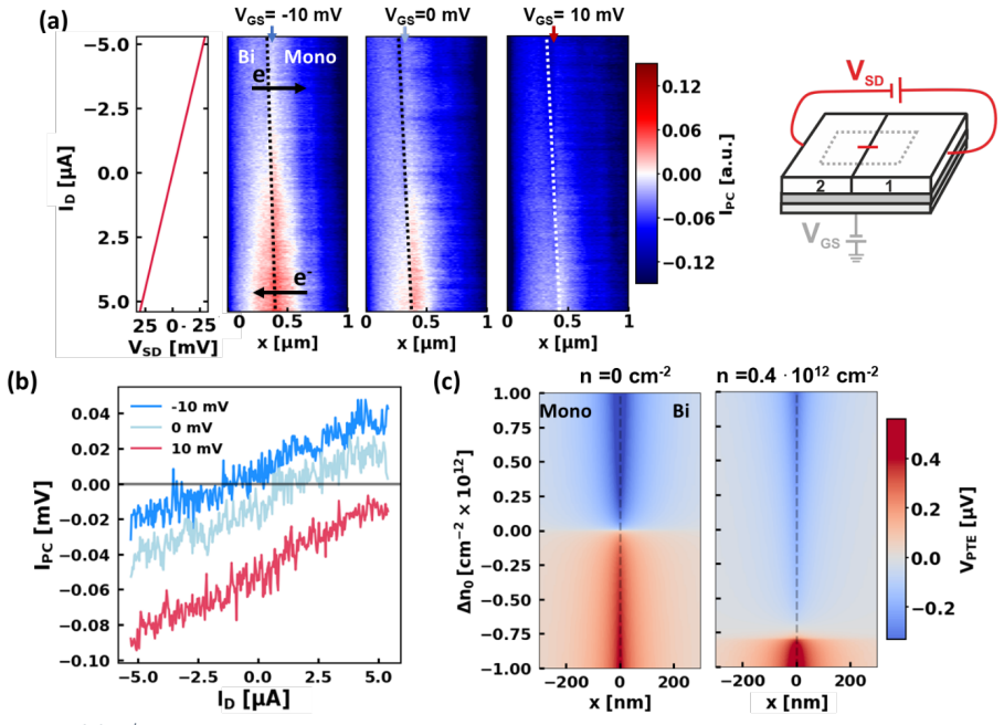
The central machinery is the combination of the monolayer–bilayer graphene interface as a one-dimensional scattering defect and the photo-thermoelectric effect as a local detector of chemical potential. In the Landauer picture, a current density j flowing past a scatterer builds a dipole p ~ j/(σ n_s), which locally shifts the carrier density; at the interface, the photocurrent is proportional to the integral of the conductivity times the spatial gradient of the Seebeck coefficient, so a density difference Δn0 across the interface produces a measurable photocurrent. The authors model this by inserting ±Δn0/2 carriers on the monolayer and ∓Δn0/2 on the bilayer in a semiclassical Boltzmann calculation of the Seebeck coefficient, and show that near the charge neutrality point a small Δn0 flips the sign of the Seebeck difference, while at higher doping it does not.
What would settle it
A decisive test would be to compare the Δn0 required by the simulations to reproduce the observed sign-switch currents with the value expected from the Landauer dipole strength p ~ j/(σ n_s) using the measured current density and conductivity. If the required Δn0 is orders of magnitude too large, or if the photocurrent sign reversal persists at higher doping when bolometric or thermal effects are independently suppressed (e.g., by measuring a device without the interface but with identical contacts), the attribution to the Landauer resistivity dipole would fail.
Extended reading notes
Core claim
The central claim is that near-field photocurrent nanoscopy can detect the Landauer resistivity dipole that forms at a one-dimensional defect during current flow. For a buried monolayer–bilayer graphene interface treated as a reflective 1D defect, the authors find that near the charge neutrality point the measured photocurrent, which is generated by the photo-thermoelectric effect and tracks the local Seebeck coefficient, follows the polarity of the applied source-drain voltage. They attribute this to a current-induced carrier density offset Δn0 across the interface—the dipole itself—which locally changes the Seebeck coefficient of each side. The effect is absent at higher carrier densities, where the same perturbation no longer produces a sign change in the Seebeck difference. Numerical simulations of the Seebeck coefficient difference ΔS as a function of total carrier density n and inserted offset Δn0 reproduce both the polarity reversal near the charge neutrality point and its disappearance at higher doping.
Load-bearing premise
The interpretation assumes that the current-induced photocurrent changes near the charge neutrality point come specifically from the carrier-density offset Δn0 produced by the Landauer dipole, rather than from any other bias-dependent process, such as bolometric heating, photovoltaic effects, or current-induced thermal gradients.
Editorial extensions
If this is right
- Landauer resistivity dipoles at one-dimensional defects can be imaged at room temperature and under ambient conditions, without contacting the defect.
- The photocurrent polarity follows the current direction only near the charge neutrality point, providing a local, gate-tunable signature of current-induced carrier accumulation.
- The same near-field photocurrent technique can be applied to other buried interfaces and defects in van der Waals heterostructures.
- Since the LRD signature disappears at high carrier density, devices operating at low conductivity are the regime where local dissipation from such dipoles becomes experimentally visible.
- The measurements support the Landauer picture that the voltage drop in a nanoscale conductor is concentrated at defects.
Reading between the lines
- One could test the quantitative LRD scaling by fixing the doping and measuring the photocurrent versus current: the dipole strength p ~ j/(σ n_s) predicts a specific linear dependence that the paper does not extract.
- The technique might be extended to map hot-electron cooling lengths or thermoelectric inhomogeneity around other defects, since the photocurrent signal encodes both the Seebeck difference and the temperature profile.
- If the LRD interpretation holds, near-field photocurrent imaging could be used as a failure-prediction tool in integrated circuits, revealing where current crowding and local heating concentrate in buried metallization.
- The paper's numerical model inserts Δn0 by hand; connecting Δn0 to the actual current distribution around the defect (e.g., via a finite-element transport simulation) would turn a qualitative match into a quantitative confirmation.
Signed reviews
Editorial analysis
A structured set of objections, weighed in public.
Referee Report
Summary. The manuscript reports near-field photocurrent nanoscopy on a monolayer-bilayer graphene interface buried under hBN, with source-drain bias and back-gate voltage varied systematically. The authors observe that near the charge neutrality point the photocurrent polarity follows the applied bias, while at higher hole or electron doping the photocurrent is independent of bias. They interpret this as real-space evidence of Landauer resistivity dipoles forming at the one-dimensional interface, with the dipole-induced carrier-density offset across the interface changing the local Seebeck coefficients and hence the photo-thermoelectric current. Numerical calculations of the Seebeck-coefficient difference and simulated photocurrent profiles are presented, based on an imposed density offset Δn0 across the junction.
Significance. If the interpretation is correct, the work would demonstrate a room-temperature, non-invasive, nanoscale probe of local dissipation at a buried interface, extending earlier low-temperature scanning tunneling potentiometry studies of Landauer resistivity dipoles to a technically more relevant regime. The experimental dataset is substantial: two samples, systematic gate and bias dependence, floating-contact control measurements, and Seebeck simulations that reproduce the zero-bias double sign switch. However, the central claim currently rests on a model in which the key quantity Δn0 is inserted by hand as an independent parameter mimicking the very effect under test, and no quantitative link is made to the measured current or to the Landauer dipole strength discussed in the text. The significance of the observation itself is clear, but the specificity of the Landauer attribution is not yet established.
major comments (4)
- [Figure 3b and the paragraph beginning 'To corroborate that a charge carrier density difference'] The model adds ±Δn0/2 carriers to the monolayer and bilayer as an independent input and the text explicitly says Δn0 'mimics' the LRD-induced density deviation. No equation connects Δn0 to the measured source-drain current, the conductivity, the scatterer density, or the dipole strength p ~ j/(σ n_s) quoted earlier in the paper. Because Δn0 is a stand-in for the very effect being tested, the agreement between the calculated sign reversal and the data is a consistency check with a free parameter rather than a quantitative prediction. The authors should derive an expected Δn0(I_D, V_GS) from the Landauer dipole potential or from the measured device resistance and compare it with the values needed in Figures 3b and 4c.
- [Section 'After having characterized the ML/BL in detail' and Figure 3a] The bolometric exclusion is argued from the observation that the photocurrent is independent of bias at high doping (V_GS = -100 mV and +150 mV). This control is not decisive, because a bolometric or Joule-heating-induced carrier-density shift is expected to be largest near the charge neutrality point, where the Seebeck coefficient varies steeply with density. The same control at the high-doping points therefore does not rule out a bias-induced thermal or bolometric contribution exactly in the region where the claimed LRD signature appears. A quantitative estimate of the expected bolometric photocurrent near the CNP, or a control measurement at low doping with a different interface or defect, would be needed to support the exclusion.
- [Figure 4c and the accompanying text] The experimental x-axis in Figure 4b is the source-drain current I_SD, while the simulation x-axis in Figure 4c is the density offset Δn0. The text compares the shift of the sign-switch crossing with total carrier density, but the paper does not establish that the I_SD-to-Δn0 conversion is the same at each gate voltage. The observed shift of the crossing current could be produced by a gate-dependent conversion factor or by a different bias-induced mechanism. Presenting the data and simulation on a common axis, or at least providing the conversion used, would make the comparison quantitative and falsifiable.
- [Equation (1) and the discussion of cooling length] The photocurrent expression (1) depends on σ(x), S(x), and the spatially varying electron temperature profile T(x). A bias-induced change in local carrier density will in general also change σ(x) and the cooling length L_c ~ sqrt(k/g) via the Wiedemann-Franz relation, which the model does not include. The model assumes that the only relevant bias effect is a uniform density offset per side of the interface; the influence of bias-induced changes in σ(x) or in the hot-carrier temperature profile on the photocurrent should be estimated, or the assumption should be justified quantitatively.
minor comments (4)
- [Throughout] The notation for the density offset is inconsistent: the text uses both 'Dn0' and 'Δn0', and the gate voltage is written as 'VGS' and 'V_GS' in different places. Please unify the notation.
- [Figure 2a caption] The caption says 'VGS varies from -1 V to 1 V in steps of 0.1 V', but the main text states the CNP is at V_GS = 0 V in Figure 2a while in Figure 4a it is at V_GS = -10 mV. Please clarify whether the gate voltages are the same scale in both figures or whether there is a difference in the reference point of the two samples.
- [Equation (1)] Equation (1) appears corrupted in the text, with stray '$' symbols and an unclear integrand and integration limits; the definition of the spatial coordinate x and the direction of integration are described in the text but should be made explicit in the equation itself.
- [Figure 3a caption] The caption states that the graph to the left shows 'ISD with respect to the VSD applied' for one of the maps, but it is not stated which map and how the y-axis and color bar are shared across the three panels; please specify the correspondence clearly.
Circularity Check
Near-CNP photocurrent sign reversal is reproduced by inserting the very density offset (Δn0) the paper aims to detect; the agreement is a consistency check with a free parameter, not an independent prediction.
-
fitted input called prediction
[Main text paragraph 'To corroborate that a charge carrier density difference Dn0...' and Figure 3b caption (pages 6-7 and Figure 3 caption, page 16)]
"The additional parameter Δn0, independent of n and mimicking the role of the deviation of the carrier density n induced by the LRD around the interface which is a consequence of the applied ID. ... In our calculation we add for each datapoint Δn0/2 carriers to the ML and - Δn0/2 to the BL. ... The measured ID dependence of IPC is indeed consistent with our calculations under the hypothesis of localized LRD formation at the ML/BL interface."
The model's only route from applied current to photocurrent is the input parameter Δn0, which the caption explicitly says 'mimics' the LRD-induced density deviation. Near the CNP, the sign of ΔS (and hence IPC) is fixed by the sign chosen for Δn0, and that sign is tied to the sign of ID by assumption, not derived from the Landauer dipole strength p ~ j/(σ n_s) given earlier in the paper. The observed sign reversal is therefore reconstructed from the hypothesis rather than predicted; any desired ID-sign dependence could be accommodated by choosing the corresponding Δn0 sign.
-
fitted input called prediction
[Figure 4c caption and concluding text of the LRD section ('Finally, the increase in IPC with increasing Δn0 (or ID)...')]
"The parameter Δn0 mimics the deviation of the carrier density n induced by the ISD - induced LRD around the interface. ... In the experiment, the Dn0 accumulation at the BL/ML interface is a consequence of the LRD."
The same free parameter is swept until the simulated sign-switch shift matches the gate-voltage trend, and that match is then used to assert that the experimental Δn0 (and the associated IPC) is a consequence of the LRD. Because Δn0 is never connected quantitatively to the measured I_D or to p ~ j/(σ n_s), the comparison is a curve-matching exercise: any bias-induced density asymmetry near the CNP (bolometric, photovoltage, or other) would produce the same ΔS structure. The LRD attribution is assumed in the input rather than established by the output.
full rationale
The Seebeck-coefficient calculation in Figure 2c is parameter-free in its essentials and independently reproduces the known double sign switch of ΔS at a monolayer/bilayer interface; that part is self-contained and non-circular. The circularity is confined to the LRD step. In Figures 3b and 4c the model inserts a carrier-density offset Δn0 that is explicitly described as 'mimicking' the LRD, then shows that this inserted offset produces an ID-dependent photocurrent near the CNP and a smaller dependence at high doping. The near-CNP sign reversal is an algebraic consequence of the sign of the inserted Δn0, so it is not an independent confirmation that a Landauer resistivity dipole has formed. The high-doping independence and the VGS-dependence of the sign-switch do provide some falsifiability, which prevents the paper from being fully circular; nevertheless, the central claim that the experiment 'detect[s] the formation of Landauer resistivity dipoles' rests on an unquantified mapping from I_D to Δn0. No load-bearing self-citation chain was found; the authors' prior works are cited for methods and standard thermoelectric expressions, not as the basis of the LRD inference. The score of 5 reflects a partial circularity: the key qualitative signature is built in by the free parameter, while the quantitative density and doping behavior retains independent content.
Assumptions & free parameters
free parameters (1)
- Δn0 (interface carrier-density offset) =
varied by hand; e.g. Δn0=-0.8e12 cm^-2 at n=0.4e12 cm^-2
assumptions (5)
- domain assumption Photocurrent is governed by the photo-thermoelectric expression I_PC = -∫ σ(x) S(x) dT/dx dx (Eq. 1).
- domain assumption The monolayer-bilayer graphene interface acts as an ideal one-dimensional reflective defect for Landauer dipole theory.
- domain assumption The Seebeck coefficient is computed in the semiclassical Boltzmann relaxation-time approximation with no density dependence of τ (Eq. 2).
- ad hoc to paper LRD-induced carrier redistribution is captured by an imposed, position-independent ±Δn0/2 density offset across the interface.
- domain assumption Bias-dependent photocurrent from bolometric or photovoltaic processes is negligible near the interface.
Cite this review
Pith. "Pith review of Landauer resistivity dipole at one dimensional defect revealed via near-field photocurrent nanoscopy." pith.science (2026). https://pith.science/paper/43AQ44TP
@misc{pith2026250109124,
  author       = {Pith},
  title        = {Pith review of: Landauer resistivity dipole at one dimensional defect revealed via near-field photocurrent nanoscopy},
  year         = {2026},
  howpublished = {\url{https://pith.science/paper/43AQ44TP}},
  note         = {Machine review of arXiv:2501.09124}
}
read the original abstract
The fundamental question how to describe Ohmic resistance at the nanoscale has been answered by Landauer in his seminal picture of the so-called Landauer resistivity dipole. This picture has been theoretically well understood, however experimentally there are only few studies due to the need for a non-invasive local probe. Here we use the nanometer lateral resolution of near-field photocurrent imaging to thoroughly characterize a buried monolayer - bilayer graphene interface as an ideal one dimensional defect for the Landauer resistivity dipole. Via systematic tuning of the overall charge carrier density and the current flow we are able to detect the formation of Landauer resistivity dipoles due to charge carrier accumulation around the one dimensional defects. We found that, for Fermi energy values near the charge neutrality point (i.e. at low hole or electron doping), the photocurrent exhibits the same polarity as the applied source-drain voltage, which is consistent with changes in carrier concentration induced by the Landauer resistivity dipoles. This signature is no longer evident at higher charge carrier density in agreement with the performed numerical calculations. Photocurrent nanoscopy can thus serve as non-invasive technique to study local dissipation at hidden interfaces.
Figures

Reference graph
Works this paper leans on
-
[10]
Direct visualization of electric current induced dipoles of atomic impurities
Korenblum, B. & Rashba, E. I. Classical properties of low-dimensional conductors: giant capacitance and non-ohmic potential drop. Phys. Rev. Lett. 89, 96803 (2002). 11. Novoselov, K. S. et al. Electric field effect in atomically thin carbon films. Science 306, 666–669 (2004). 12. Novoselov, K. S. et al. Two-dimensional gas of massless Dirac fermions in gr...
work page Pith review arXiv 2002
-
[30]
Geisenhof, F. R. et al. Interplay between topological valley and quantum Hall edge transport. Nat. Commun. 13, 4187 (2022). 31. Woessner, A. et al. Near-field photocurrent nanoscopy on bare and encapsulated graphene. Nat. Commun. 7, 10783 (2016). 32. Rikhter, A., Basov, D. N. & Fogler, M. M. Modeling of plasmonic and polaritonic effects in photocurrent na...
arXiv 2022
-
[49]
Hwang, E. H. & Das Sarma, S. Screening, Kohn anomaly, Friedel oscillation, and RKKY interaction in bilayer graphene. Phys. Rev. Lett. 101, 156802 (2008). 50. Tielrooij, K.-J. et al. Out-of-plane heat transfer in van der Waals stacks through electron-hyperbolic phonon coupling. Nat. Nanotech. 13, 41–46 (2018). 51. Nam, S.-G., Ki, D.-K. & Lee, H.-J. Thermoe...
work page 2008
Reviewed August 10, 2026 · model on record in the stance chip above.
Discussion (0). Continue with ORCID to comment.