REVIEW 4 major objections 5 minor 1 cited by
Optimizing CMOS-compatible, superconducting titanium nitride resonators: Deposition conditions and structuring processes
T0 review · 4 major / 5 minor · reviewed 2026-08-02 · deepseek-v4-flash
Pith's one-line read Process-induced surface oxides, not the TiN crystal orientation, dominate low-power microwave loss in superconducting TiN resonators, and a buffered-oxide-etch dip removes them to reach loss values near 10^-6.
desk verdict A careful 200-mm TiN process study with a striking BOE recovery result, but the oxide-dominance claim rests on inferential assumptions that need more evidence. read the letter →
The pith
A machine-rendered reading of the paper's core claim, the machinery that carries it, and where it could break.
The reading
What carries the argument
The electro-magnetic participation-ratio model, which decomposes resonator TLS loss into contributions from four regions — silicon bulk (Si), metal–substrate (MS), metal–air (MA), and substrate–air (SA) interfaces — each weighted by the fraction of electric-field energy stored in that region (Eqs. 4 and 5). The key move is keeping the CPW geometry (10-µm signal line, 6-µm gap, ~150-nm TiN) fixed across all process variants, so participation ratios remain nearly constant and measured loss changes can be traced to interface modifications. Finite-element simulations for the expected 0–100-nm overetch depths show only small participation-ratio shifts, supporting this attribution.
What would settle it
Fabricate BOE-treated resonators with a deliberately varied metal–substrate interface — for example, a different pre-deposition silicon clean or a thin interfacial layer — and measure TLS loss with a two-hour time-coupled cooldown; if the loss changes noticeably, the MS interface is not constant and the oxide-dominance attribution is incomplete.
Extended reading notes
Core claim
The central claim is that lossy surface oxides at the MA and SA interfaces are the dominant TLS loss channels, and that removing them with a BOE wet etch recovers the etch-induced losses, making the prior etch and strip history irrelevant. This is shown by the convergence of the worst-performing (high-power etch, high-temperature strip) and best-performing (low-power etch, low-temperature strip) process combinations to the same loss level after BOE treatment, and by the further reduction to median δTLS = 9.67×10^-7 and δLP = 11.04×10^-7 with a two-hour time-coupled cooldown. The paper also claims that all three TiN orientations reach similar minimal losses when the surface is cleaned, with t
Load-bearing premise
The claim depends on the unquantified assumption that the metal–substrate interface and silicon bulk losses remain constant across all process variants, so every measured loss change can be assigned to the metal–air and substrate–air interfaces.
Editorial extensions
If this is right
- A single BOE wet dip can undo the TLS losses introduced by aggressive etch and strip processes, so the prior structuring history no longer determines resonator quality.
- Optimization effort should shift from TiN deposition texture to surface and interface treatments, since processing dominates over crystal orientation.
- TiN(111) films are the safer choice when surface treatment or cooldown timing is not tightly controlled, because they reoxidize more slowly.
- The combination of BOE and time-coupled cool-down yields internal quality factors approaching one million in a 200-mm CMOS-compatible flow.
- Room-temperature reoxidation saturates quickly, with no substantial growth between 2 and 24 hours after BOE treatment.
Reading between the lines
- If MA/SA oxides are indeed the limiting hosts, then passivating the resonator surface with a non-oxidizing cap immediately after BOE could push TLS loss below the 9.67×10^-7 value reported here — an extension the paper does not test.
- The same oxide-removal logic may transfer to other CMOS-compatible superconducting metals such as niobium or aluminum, whose surfaces also oxidize during processing, although the paper demonstrates it only for TiN.
- The attribution assumes a constant MS interface; because the low-power etch produces an undercut and rough sidewalls, the simulations (for vertical trenches only) may not capture the true field distribution, so some loss currently assigned to MA/SA could belong to MS or sidewall regions.
- A practical consequence for qubit fabrication: integrating a BOE step and controlled cooldown timing into the packaging flow may be more effective than trying to prevent oxide growth during earlier etch steps.
Editorial analysis
A structured set of objections, weighed in public.
Referee Report
Summary. The paper reports a systematic 200 mm CMOS-compatible fabrication study of superconducting TiN CPW resonators. Three sputter deposition processes yield TiN(111), TiN(200), and mixed orientations; each is combined with high/low power dry etching and high/low temperature in-situ resist stripping, with a buffered oxide etch (BOE) post-treatment for selected samples. Cryogenic loss measurements are analyzed with the standard TLS saturation model, Eq. (3), and participation-ratio simulations, Eq. (4)-(5). The central claims are that the structuring process, not the TiN film orientation, dominates the TLS loss; that low-power etch plus low-temperature strip gives the best result; that lossy process-induced oxides at the metal-air (MA) and substrate-air (SA) interfaces are the dominant loss channels; and that a BOE dip removes these oxides and makes the loss independent of prior etch/strip history, reaching median δ_TLS = 9.67×10^-7 and δ_LP = 11.04×10^-7.
Significance. The result, if fully established, has clear practical value for industrial superconducting-qubit fabrication: it identifies a scalable BOE-based recovery step and demonstrates that the TiN crystal orientation is not the primary loss bottleneck. The study has genuine strengths: a controlled 200 mm process matrix with nominally identical resonator geometry, statistical reporting through medians and IQRs, and a striking experimental observation that HP/HT and LP/LT samples converge after BOE treatment. These are important data for the CMOS-compatible quantum-hardware community. However, the paper's mechanistic conclusion about oxide identity and the MA/SA decomposition goes beyond what the current measurements uniquely establish, so the version as written needs revision.
major comments (4)
- [Sec. III B 2] The load-bearing assumption 'we can assume that the TLS loss at the MS interface also remains constant within each deposition process' is not quantified. The LP etch is described in Sec. III A 2 and Fig. 6 as producing undercut near the TiN/Si interface and rough sidewalls, so the MS-region geometry and its chemical environment are not identical between HP and LP samples. Table IV gives participation ratios only for vertical overetch depths of 0-100 nm with an assumed 2 nm interfacial layer; the LP undercut and sidewall roughness are not modeled. Consequently, changes in p_MS δ_MS, or in the local participation ratio, could masquerade as MA/SA loss changes. Please either bound this effect with simulations that include the LP undercut/roughness, or add an experiment that varies the etch while holding the MS geometry fixed.
- [Sec. III B 3 and Fig. 10] The BOE experiment is interpreted as proof that process-induced oxides at the MA and SA interfaces are the dominant loss channels. BOE, however, removes any acid-soluble surface layer, including amorphous silicon damage, etch-polymer residues, and N-depleted TiN, all of which are plausible products of the HP/HT process. The convergence of HP/HT and LP/LT after BOE is equally consistent with the removal of a universal damaged surface layer. Without surface chemical-state analysis (e.g., XPS, AES, or calibrated ellipsometry with chemical verification) of the MA and SA interfaces before and after BOE, the attribution of the recovered loss specifically to oxide removal is not uniquely established. At minimum, a control treatment that removes damage but not oxide, or vice versa, would address this.
- [Sec. III B 2 and III B 3] The text first states, for the etch process, that 'Distinguishing between these two effects is not possible with the current setup' and later infers that 'the majority of the contribution to the losses originates from the MA interface region'. These statements are in tension. The SA interface is directly modified by the etch (roughness, amorphization, and oxidation) and by the strip (ellipsometry shows oxide thickness increasing from 0.5 nm to 3.2 nm), so the measured differences between HP and LP, or HT and LT, do not by themselves identify MA as the larger contributor. Please either remove the majority-MA inference or support it with a dedicated experiment (e.g., independent modification of the top surface versus the substrate surface).
- [Sec. III B 3] The BOE series was performed exclusively on TiNmixed films, as stated in the text, yet the abstract and conclusion generalize the BOE-based recovery and the 'reoxidation robustness' narrative to the TiN111 and TiN200 films. Given that the paper itself argues the orientations differ in oxidation robustness, the generalization needs either supporting data for the other two orientations or an explicit limitation statement confining the BOE claim to TiNmixed films.
minor comments (5)
- [Abstract] Typo: 'depositons' should be 'depositions'.
- [Sec. II D] The sentence 'A smaller RRR value implies ... low defect density' is inverted; a smaller RRR implies a larger residual resistance relative to the room-temperature resistance, i.e., more defect scattering. The subsequent discussion of TiN111's high RRR assumes the correct direction.
- [Fig. 8 caption] The caption says 'HP etch with HP strip'; the text and the relevant process combination use HT strip. Please correct.
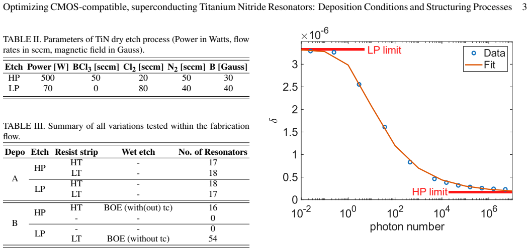
- [Table III] The formatting of rows for Depo B is confusing (some cells are empty, some contain only '-' or '0'); please clarify which process combinations were actually fabricated and measured.
- [Conclusion] The conclusion says 'in-plane orientations' for the (111) and (200) textures, whereas the XRD 2θ/ω analysis in Sec. III A 1 provides out-of-plane orientation information. Please correct the wording.
Circularity Check
No significant circularity: measured TLS losses and BOE comparisons are independent of the conclusions.
full rationale
The paper's central quantities, δTLS and δLP, are measured directly from resonator transmission using the standard TLS saturation fit, Eq. (3), with Eq. (2) defining δTLS = δLP − δHP. The BOE experiment is an interventional before/after comparison of these measured values, not a model-based prediction that uses the outcome as an input. The participation ratios in Table IV are computed independently via HFSS for the resonator geometry, and the conclusion that MA/SA interface oxides dominate is supported by controlled variation of etch power and strip temperature, plus the convergence of HP/HT and LP/LT samples after BOE. The assumption that δSi and δMS remain constant across process variations is an empirical invariance assumption, not a definitional identity or a fitted-parameter tautology; it is stated explicitly and is a legitimate—though debatable—scientific assumption. Self-citations [6] and [34] appear only as literature context and general statements that oxides host TLS; they are not load-bearing. The caveats noted in the paper—e.g., that SA and MA effects cannot be fully distinguished and that BOE could also remove non-oxide damage—are evidence-strength limitations, not circular reasoning. No equation is equivalent to another by construction, and no fitted parameter is renamed as a prediction. Therefore the derivation chain is self-contained with respect to circularity.
Assumptions & free parameters
free parameters (3)
- TLS saturation exponent β (Eq. 3) =
per resonator fit
- Critical photon number nc =
per resonator fit
- Interfacial layer thickness for participation ratios =
2 nm for MA, SA, MS
assumptions (6)
- domain assumption TLS loss follows a broad-distribution saturation model Eq. (3) in the T→0 limit
- domain assumption Total TLS loss is the participation-weighted sum of interface and substrate loss tangents (Eq. 5)
- domain assumption Substrate loss δ_Si is constant across all process variations (high-resistivity >3500 Ωcm)
- domain assumption MS-interface loss is constant within each deposition process
- ad hoc to paper Participation ratios for 0–100 nm overetch are well approximated by vertical-wall HFSS with 2 nm interfacial layers
- domain assumption Reoxidation saturates between 2 and 24 h after BOE; 2 h time-coupling captures the low-loss state
Cite this review
Pith. "Pith review of Optimizing CMOS-compatible, superconducting titanium nitride resonators: Deposition conditions and structuring processes." pith.science (2026). https://pith.science/paper/OPVGMSSP
@misc{pith2026260300441,
  author       = {Pith},
  title        = {Pith review of: Optimizing CMOS-compatible, superconducting titanium nitride resonators: Deposition conditions and structuring processes},
  year         = {2026},
  howpublished = {\url{https://pith.science/paper/OPVGMSSP}},
  note         = {Machine review of arXiv:2603.00441}
}
abstract
We report on the fabrication and characterization of superconducting coplanar waveguide (CPW) resonators based on titanium nitride (TiN) thin films deposited on 200\,mm diameter high-resistivity Si(100) substrates. We systematically investigate how deposition conditions, dry-etch power and in-situ resist strip temperature affect morphology, superconducting properties and dielectric losses. By tuning reactive sputtering conditions, three distinct preferred out-of-plane crystal orientations - (111), (200), and a mix of both are achieved. Our results demonstrate that all films exhibit similar minimal two-level system (TLS) losses, with TiN111 exhibiting the lowest median TLS losses $\tilde{\delta}_\mathrm{TLS}$, and greater robustness against reoxidation. The applied structuring process, in contrast, has a far greater influence on the TLS loss than the crystal orientation of the TiN film and, consequently, the intrinsic material properties of the superconducting layer. The lowest TLS losses for all TiN depositions were achieved with a low power etch and low temperature resist strip. An additional buffered oxide etch (BOE) treatment could remove high-loss interfacial oxides at the metal-air (MA) and substrate-air (SA) interface and recover the etch-induced TLS losses. Consequently, TiN resonators exhibiting $\tilde{\delta}_\mathrm{TLS}$ values as low as $9.67 \times 10^{-7}$ were realized. The corresponding median low-power loss, $\tilde{\delta}_\mathrm{LP}$, amounts to $11.04 \times 10^{-7}$, which translates to an internal quality factor approaching one million. These findings highlight the critical role of process induced oxide formation at the MA and SA interfaces in limiting the performance of TiN resonators and provide a scalable, low-loss process compatible with industry-grade 200\,mm CMOS qubit fabrication workflows.
Figures


Figures from the paper (6 more)


Forward citations
Cited by 1 Pith paper
-
Substrate-metal interface engineering enhances TaN/Ta thin film superconducting resonator performance
A thin Ta buffer between Si and a TaN seed layer nearly quadruples the internal quality factor of superconducting coplanar waveguide resonators by suppressing nitrogen-induced interface disorder.
Reference graph
Works this paper leans on
-
[1]
The resulting twelve wafers are characterized using sheet resistance measurements to deter- mine the uniformity and the reproducibility of the process
TiN deposition characterization For each of the three sputter processes (A, B, and C), four wafers are being deposited. The resulting twelve wafers are characterized using sheet resistance measurements to deter- mine the uniformity and the reproducibility of the process. Ta- ble V summarizes the mean of all sheet resistances measured on the batch and its ...
-
[2]
The influence of the strip process (here the HT strip) is not visible in the SEM images; its microscopic effects will be discussed below
TiN structuring characterization Figure 6 shows TiN films after two different structuring processes have been applied, whose parameters are described in Table II. The influence of the strip process (here the HT strip) is not visible in the SEM images; its microscopic effects will be discussed below. The HP recipe produces steep, well- defined sidewalls. T...
-
[3]
Figure 7 sum- marizes the first two of these three parameters
Influence of TiN material The first part of the cryogenic characterization focuses on analyzing the influence of the TiN material on the RRR value, Tc, and the quality factor of the resonators. Figure 7 sum- marizes the first two of these three parameters. It is evident that all films have a residual resistance ratio (RRR) greater than 1, which is typical...
-
[4]
For this purpose, Figure 9 summarizesδ TLS for all four process combinations derived from pairing LP and HP etching with LT and HT resist stripping
Influence of structuring processes The focus now shifts to examining the influence of the structuring processes on the TLS and LP loss of the respec- tive resonators. For this purpose, Figure 9 summarizesδ TLS for all four process combinations derived from pairing LP and HP etching with LT and HT resist stripping. The median for both, TLS and LP losses, a...
-
[5]
Powder Diffraction File® Card No. 00-038-1420 for Titanium Nitride (TiN),
Influence of BOE wet etching and time coupling The final experimental series investigates the post- treatment with a wet etch using BOE and its effect on the loss tangents. Since the TiNmixed films tend to span the range of quality factors expected for TiN111 and TiN200 films, this experiment was conducted exclusively with TiN- mixed films. The process co...
arXiv 2012
Reviewed August 2, 2026 · model on record in the stance chip above.
Discussion (0). Continue with ORCID to comment.