REVIEW 4 major objections 5 minor 35 references
Gate Control of g-factor in Germanium Quantum Dots: A Strain-Based Explanation
T0 review · 4 major / 5 minor · reviewed 2026-08-16 · deepseek-v4-flash
Pith's one-line read Device-induced thermal-contraction strain creates a spatially varying g-tensor landscape that explains why germanium qubit g-factors swing by more than 80% under gate voltage changes.
desk verdict A plausible strain-based mechanism for gate-tunable g-factors in Ge hole qubits, but the headline percentages hinge on an undefined parameter (κ) and an unvalidated pointwise-averaging step; worth serious review after those are fixed. read the letter →
The pith
A machine-rendered reading of the paper's core claim, the machinery that carries it, and where it could break.
The reading
What carries the argument
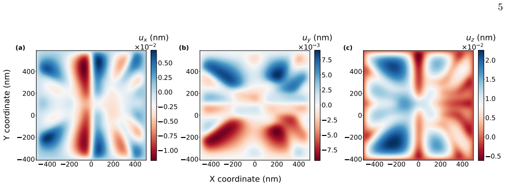
The central object is the strain-induced g-tensor correction field, a spatially nonuniform tensor $\delta g(\mathbf{r})$ obtained from the local strain components through the correction formulas of Eqs. (9)-(12). The argument is carried by a chain: a finite-element solution of the linear thermoelasticity equation gives the displacement and hence the strain; the strain corrections are divided by the heavy-hole/light-hole gap $\Delta_{\mathrm{LH}}$; a Schrödinger-Poisson hole wavefunction, fit to a three-dimensional Gaussian, averages the correction over the dot; and the effective g-factor vector is formed as $\delta \vec{g}^{\,*} = \delta g \cdot \vec{B}/B$. The last identity is the pivot: even though the out-of-plane corrections $\delta g_{zx}$ and $\delta g_{zy}$ are individually below 1% of the unstrained $g_\perp$, an in-plane magnetic field mixes them into the measured response, so the large swings are not simply echoes of the in-plane strain components.
What would settle it
Measure the effective g-factor of a single germanium dot as a function of in-plane magnetic field azimuth at fixed gate voltages and compare the resulting map with Fig. 10; the predicted 80% range for a single dot and 150% swing for a singlet-triplet qubit are sharp signatures. A cleaner control is a device whose gate metal has nearly the same thermal expansion as germanium, where the model predicts gate-voltage g-factor tunability should largely disappear.
Extended reading notes
Core claim
The paper's central discovery is that the observed gate tunability of the g-factor in germanium hole spin qubits can be accounted for without invoking any change in the material's intrinsic spin properties. Device-induced strain, arising from differential thermal contraction of the aluminum gates, the Al$_2$O$_3$ cap, and the Ge/GeSi heterostructure as the device is cooled from 300 K to 20 K, produces a spatially varying g-tensor correction whose components are proportional to local strain differences and shear strains divided by the heavy-hole/light-hole splitting $\Delta_{\mathrm{LH}}$. The hole wavefunction, computed from a Schrödinger-Poisson solver and approximated as a three-dimensional Gaussian, averages these corrections over the dot. Because gate voltages move the dot through the strain landscape, the averaged corrections change; the in-plane correction components $\delta g_{xx}$ and $\delta g_{xy}$ are of the same order as the unstrained in-plane g-factor $g_\parallel = 0.15$, and through the relation $\delta \vec{g}^{\,*} = \delta g \cdot \vec{B}/B$, the out-of-plane corrections $\delta g_{zx}$ and $\delta g_{zy}$ mix into the in-plane response. The result is that single-dot and singlet-triplet effective g-factors swing by over 80% and more than 150%, respectively, across the explored gate-voltage and field-angle range; within a 0.3 V gate change and a $\pi/2$ field rotation, the swings are about 60% and a factor of two.
Load-bearing premise
The load-bearing premise is that the strain-induced g-tensor correction formulas used here, including the unspecified coefficient $\kappa$ in Eqs. (9)-(12), remain quantitatively accurate when the local strain is averaged over a Gaussian hole wavefunction in the sharply inhomogeneous strain field directly under the gates.
Editorial extensions
If this is right
- A 0.3 V change in the middle barrier gate combined with a $\pi/2$ rotation of the in-plane magnetic field can change a single dot's effective g-factor by about 60% and a singlet-triplet qubit's by a factor of two relative to $g_\parallel = 0.15$.
- Because the correction is a wavefunction average over the strain landscape, the qubit frequency's sensitivity to gate noise is itself position-dependent, and moving the dot to a strain extremum or saddle point can suppress or amplify that sensitivity.
- The model produces the non-monotonic dependence of the singlet-triplet g-factor on barrier gate voltage seen in the experiments, indicating that strain, rather than an intrinsic electrostatic effect, underlies that behavior.
- Contour lines in the voltage-versus-field-angle plane give practical recipes for holding the g-factor constant while tuning the dot, or for deliberately sweeping the qubit frequency over a wide range.
- Strain becomes an engineering variable: choosing gate materials, layer thicknesses, and operating temperature changes the thermal-contraction strain pattern and therefore the achievable g-factor tunability in a predictable way.
Reading between the lines
- If this mechanism is correct, a device whose gate metal has nearly the same thermal expansion coefficient as germanium should show strongly suppressed gate-voltage g-factor tunability; the paper does not state this prediction, but it follows directly from the thermal-contraction origin of the strain.
- The same mechanism implies that thermal history could matter: repeated cooling cycles or different cooling rates might change the residual strain field and slightly shift qubit frequencies, so a device's g-factor map may not be perfectly reproducible run to run.
- Wider quantum dots should average over more of the strain landscape and show smaller g-factor swings, so measuring g-factor tunability versus dot size is a testable way to distinguish wavefunction averaging over strain from other mechanisms.
- Because the simulated strain pattern inherits the x-reflection symmetry of the gate layout, breaking that symmetry or choosing an asymmetric magnetic-field angle should produce left-right asymmetric tunability that could be used to address individual dots in a pair.
Signed reviews
Editorial analysis
A structured set of objections, weighed in public.
Referee Report
Summary. The manuscript proposes that the strong gate-voltage tunability of hole g-factors in germanium quantum dots is caused by device-induced thermal-contraction strain. The authors solve a 3D thermoelastic finite-element problem for a realistic multilayer gate stack, extract inhomogeneous strain fields with magnitudes of order 1e-4, combine these with strain-induced g-tensor corrections taken from Refs. [12,16], and average the corrections over hole wavefunctions obtained from the MaSQE Schrödinger-Poisson solver and then approximated as multivariate Gaussians. For a range of Brm gate voltages and in-plane magnetic-field orientations, they report that the effective g-factor of a single dot varies by over 80% and that of a singlet-triplet qubit by more than 150%, with features such as non-monotonic gate-voltage dependence. The paper frames this as a quantitative explanation of the gate-tunable g-factor observed in recent germanium qubit experiments.
Significance. If the quantitative result held, this would be an important contribution: it would connect an experimentally observed qubit parameter (gate-tunable g-factor) to a concrete physical mechanism (inhomogeneous thermal-contraction strain) and would identify in-plane g-tensor averaging as design-relevant. The paper has genuine strengths: it is a device-scale forward simulation rather than a fit to the target experiment, the strain magnitudes are checked against x-ray measurements, the δg formulas are imported from prior theory rather than tuned here, and the boundary-condition choice is benchmarked against Ref. [12]. However, the headline numbers currently rest on an undefined coefficient κ and on a pointwise application of uniform-strain formulas, so the central quantitative claim is not yet established. The paper also does not quantitatively compare its predicted sensitivity with the experimental one it claims to explain.
major comments (4)
- [Section III.B, Eqs. (9)-(12)] The coefficient κ appearing in Eqs. (9) and (12) is never defined anywhere in the manuscript, and the text as typeset uses a lower-case k in Eqs. (10) and (11). No numerical value, material parameter, or reference is given. Because the diagonal correction δgxx and the off-diagonal correction δgxy are both linear in this coefficient, every reported percentage change in Fig. 9 and Fig. 10 scales with κ. The authors must state what κ is (for example, the Luttinger Zeeman parameter), give its value, and cite its source; otherwise the central quantitative claim is unreproducible.
- [Section IV.B and IV.E] The g-tensor correction is computed pointwise from uniform-strain formulas, Eqs. (7)-(12), and then averaged over a Gaussian hole wavefunction, but the simulated strain varies by about 30% across the 16-nm well (Fig. 4) and on lateral scales of tens of nanometers, i.e., on the same scale as the dot wavefunction. The paper provides no convergence test and no comparison against a direct solution of the inhomogeneous Luttinger-Kohn Hamiltonian, Eq. (4), in the simulated strain field. It is therefore not demonstrated that the pointwise uniform-strain approximation is quantitatively accurate; this directly affects the 80% and 150% figures presented in Section V.
- [Section III.C and Section V] The gate operating points are explicitly selected by 'tun[ing] the gate voltages in order to move the dots into regions of large g-factor correction,' and the plotted Brm range (0.4-0.7 V) is then the range over which the effect is largest. The authors should show that this voltage range corresponds to the experimentally relevant operating range and report how the predicted sensitivity changes if a broader or unbiased range of gate voltages is used. Without this, the strength of the predicted tunability may be an artifact of the chosen operating window rather than a robust property of the device.
- [Section V and Fig. 10] The paper claims that the mechanism 'may account for' the experimentally observed tunability, but it makes no quantitative comparison with the experiment in Ref. [9], which reports a nearly order-of-magnitude change in the singlet-triplet qubit frequency for a 12 mV change in a barrier gate. In contrast, the model shown in Fig. 10(c) gives roughly a factor-of-two change over a 0.3 V range of Brm. The authors should compare the predicted and measured sensitivity in common units (e.g., fractional change per mV) and discuss any discrepancy, or they should moderate the claim from 'quantitative explanation' to a proof-of-principle mechanism.
minor comments (5)
- [Section IV.E and Fig. 7/8] The text refers to 'Fig. 8' twice when describing the z-direction projection of the hole density and then again for the horizontal planar cross-section; the figure numbers appear to be mismatched, with Fig. 7 being the z-direction profile and Fig. 8 the planar cross-section.
- [Section V, after Eq. (16)] The sentence 'expanding Eq. (3)' appears to refer to the effective g-factor definition, Eq. (14), not to the weak-form equation Eq. (3); please correct the cross-reference.
- [Section III.C] There is a typo in 'tuned for for each value'; the word 'for' is repeated.
- [Section IV.D] The text says the g-tensor correction is calculated 'using Eq. 9', but Fig. 6 shows all four correction components, which require Eqs. (9)-(12); please clarify.
- [Conclusion] The Conclusion states that within a 0.3 V gate change and a π/2 rotation of the in-plane field the singlet-triplet g-factor changes by a factor of 2, whereas Section V reports a 145% change for Brm from 0.4 to 0.55 at fixed φ=3π/2; these statements should be reconciled or explicitly distinguished.
Circularity Check
No significant circularity: the g-factor variations are forward-computed from external strain-correction formulas, FEM strain fields, and Schrödinger–Poisson wavefunctions, with no parameter fitted to the target experiment.
full rationale
The paper's derivation chain is a forward simulation. Thermal-contraction strain is obtained by solving the thermoelasticity equation (Eqs. 1–3) with literature material parameters and a stated boundary condition, not by tuning to the target g-factor data. The g-tensor corrections in Eqs. (9)–(12) are imported from external prior work (Refs. [12,16]) and used as given; the deformation potentials are taken from Table IV. Hole wavefunctions come from a Schrödinger–Poisson solver (Ref. [17], a code/method reference), and the g-factor expectation values are computed by averaging the strain-induced corrections over those wavefunctions. The effective g-factors in Fig. 10 are then obtained from Eq. (16) using the unstrained g-values g⊥=13.5 and g∥=0.15 taken from Ref. [12]. No constant is fitted to the experimental g-factor modulation the paper seeks to explain, and no prediction is defined in terms of the target observable. The choice to tune gate voltages into regions of large correction (Section III C) selects an operating range that can enlarge the reported effect, but it is an input choice, not an equation-level reduction: the computed g-factor changes are still derived from the strain and wavefunction calculations rather than being equivalent to the inputs by construction. The undefined κ in Eqs. (9)–(12) is a reproducibility and validation concern, not a circularity. There is no load-bearing self-citation chain, and no uniqueness theorem is imported from the present authors' prior work. Therefore the derivation is self-contained and no circular step is exhibited.
Assumptions & free parameters
free parameters (1)
- κ (coefficient in the strain-induced g-tensor corrections) =
not specified in text
assumptions (4)
- domain assumption Weak coupling: the temperature field is unaffected by mechanical deformation, so the thermal contraction strain can be solved from the temperature difference alone (Appendix B.2).
- domain assumption The strain-induced g-tensor corrections of Refs. [12,16], Eqs. (9)-(12), are quantitatively correct when averaged over the hole wavefunction.
- ad hoc to paper The hole probability density is well represented by a multivariate Gaussian when computing the g-tensor expectation value (Section IV E).
- standard math Small-strain linear elasticity, keeping only first-order terms in the strain-displacement relation (Eq. A4).
Cite this review
Pith. "Pith review of Gate Control of g-factor in Germanium Quantum Dots: A Strain-Based Explanation." pith.science (2026). https://pith.science/paper/7W5YB5XK
@misc{pith2026260812718,
  author       = {Pith},
  title        = {Pith review of: Gate Control of g-factor in Germanium Quantum Dots: A Strain-Based Explanation},
  year         = {2026},
  howpublished = {\url{https://pith.science/paper/7W5YB5XK}},
  note         = {Machine review of arXiv:2608.12718}
}
read the original abstract
The g-factor is a key parameter governing the behavior of semiconductor spin qubits, as it directly determines the qubit frequency and its sensitivity to electrical and magnetic noise. Recent experiments in germanium quantum dots have revealed large g-factor variations under small gate voltage changes, indicating a strong coupling between electrostatics and spin properties. Here, we present a quantitative explanation based on strain-induced g-tensor modulation. By combining finite-element simulations of inhomogeneous strain with quantum calculations of hole wavefunctions, we show that device-induced strain produces spatially varying g-tensors. Gate voltages shift the quantum dot within this landscape, leading to substantial changes in the effective g-factor. Our results may account for the experimentally observed tunability and highlight the importance of in-plane g-tensor variations. This work establishes a direct link between strain, electrostatic control, and qubit performance in germanium spin qubits.
Figures


Figures from the paper (8 more)


Reference graph
Works this paper leans on
-
[12]
J. C. Abadillo-Uriel, E. A. Rodr´ ıguez-Mena, B. Martinez, and Y.-M. Niquet, Hole-spin driving by strain-induced spin-orbit interactions, Physical Review Letters131, 097002 (2023)
work page 2023
- [9]
-
[1]
Watzinger, J
H. Watzinger, J. Kukuˇ cka, L. Vukuˇ si´ c, F. Gao, T. Wang, F. Sch¨ affler, J.-J. Zhang, and G. Katsaros, A germanium hole spin qubit, Nature Communications9, 3902 (2018)
2018
-
[2]
E. A. Chekhovich, M. Hopkinson, M. S. Skolnick, and A. I. Tartakovskii, Suppression of nuclear spin bath fluctuations in self-assembled quantum dots induced by inhomogeneous strain, Nature Communications6, 6348 (2015)
work page 2015
-
[3]
G. Scappucci, C. Kloeffel, F. A. Zwanenburg, D. Loss, M. Myronov, J.-J. Zhang, S. De Franceschi, G. Katsaros, and M. Veldhorst, The germanium quantum information route, Nature Reviews Materials 610, 926–43 (2020)
work page 2020
-
[4]
C. Kloeffel, M. Trif, and D. Loss, Strong spin-orbit interaction and helical hole states in ge/si nanowires, Phys. Rev. B84, 195314 (2011)
work page 2011
-
[5]
D. M. Zajac, A. J. Sigillito, M. Russ, F. Borjans, J. M. Taylor, G. Burkard, and J. R. Petta, Resonantly driven cnot gate for electron spins, Science359, 439 (2018)
2018
-
[6]
J. R. Petta, A. C. Johnson, J. M. Taylor, E. A. Laird, A. Yacoby, M. D. Lukin, C. M. Marcus, M. P. Hanson, and A. C. Gossard, Coherent manipulation of coupled electron spins in semiconductor quantum dots, Science 309, 2180 (2005)
2005
Show all 35 references
-
[7]
Burkard, T
G. Burkard, T. D. Ladd, A. Pan, J. M. Nichol, and J. R. Petta, Semiconductor spin qubits, Reviews of Modern Physics95, 025003 (2023)
2023
-
[8]
Jirovec, A
D. Jirovec, A. Hofmann, A. Ballabio, P. M. Mutter, G. Tavani, M. Botifoll, A. Crippa,et al., A singlet-triplet hole spin qubit in planar ge, Nature Materials20, 1106 (2021)
2021
-
[10]
N. W. Hendrickx, L. Massai, M. Mergenthaler, F. J. Schupp, S. Paredes, S. W. Bedell, G. Salis, and A. Fuhrer, Sweet-spot operation of a germanium hole spin qubit with highly anisotropic noise sensitivity, Nature Materials23, 920 (2024)
2024
-
[11]
V. P. Michal, B. Venitucci, and Y.-M. Niquet, Longitudinal and transverse electric field manipulation of hole spin-orbit qubits in one-dimensional channels, Physical Review B103, 045305 (2021)
2021
-
[13]
L. D. Landau, E. M. Lifshitz, A. M. Kosevich, E. Lifshitz, and L. P. Pitaevskii,Theory of Elasticity: Volume 7, Course of Theoretical Physics (Elsevier, 1986). 11 0.7 0.6 0.5 0.4 0 4 2 3 4 5 4 3 2 7 4 2 (a) 0.7 0.6 0.5 0.4 0 4 2 3 4 5 4 3 2 7 4 2 (b) 0.7 0.6 0.5 0.4 0 4 2 3 4 ...
1986
-
[14]
J. M. Luttinger and W. Kohn, Motion of electrons and holes in perturbed periodic fields, Phys. Rev.97, 869 (1955)
1955
-
[15]
Willatzen and L
M. Willatzen and L. C. Lew Yan Voon,The k p Method: Electronic Properties of Semiconductors (Springer Berlin, Heidelberg, 2009) eBook ISBN: 978-3-540-92872-0, Published: 06 June 2009, Hardcover ISBN: 978-3-540-92871-3, Published: 23 June 2009, Softcover ISBN: 978-3-642-10090-1...
2009
- [16]
-
[17]
C. R. Anderson, Efficient solution of the schroedinger–poisson equations in layered semiconductor devices, Journal of Computational Physics228, 4745 (2009)
2009
-
[18]
C. C. D. Frink, B. D. Woods, M. P. Losert, E. R. MacQuarrie, M. A. Eriksson, and M. Friesen, Reducing strain fluctuations in quantum dot devices by gate-layer stacking, arXiv (2024), arXiv:2312.09235
2024
-
[19]
Corley-Wiciak, C
C. Corley-Wiciak, C. Richter, M. H. Zoellner, I. Zaitsev, C. L. Manganelli, E. Zatterin, T. U. Sch¨ ulli,et al., Nanoscale mapping of the 3d strain tensor in a germanium quantum well hosting a functional spin qubit device, ACS Applied Materials & Interfaces15, 3119 (2023)
2023
-
[20]
J. C. Abadillo-Uriel, E. A. Rodrıguez-Mena, B. Martinez, and Y.-M. Niquet, Supplementary material for ‘hole spin driving by strain-induced spin-orbit interactions’, n.d
-
[21]
Taboga, Properties of eigenvalues and eigenvectors (2021), lectures on Matrix Algebra
M. Taboga, Properties of eigenvalues and eigenvectors (2021), lectures on Matrix Algebra
2021
-
[22]
Bleyer,Numerical Tours of Computational Mechanics with FEniCS(2018)
J. Bleyer,Numerical Tours of Computational Mechanics with FEniCS(2018)
2018
-
[23]
M. S. Alnaes, J. Blechta, J. Hake, A. Johansson, B. Kehlet, A. Logg, C. Richardson, J. Ring, M. E. Rognes, and G. N. Wells, The fenics project version 1.5, Archive of Numerical Software3, 10.11588/ans.2015.100.20553 (2015)
2015 doi
-
[24]
Saad and M
Y. Saad and M. H. Schultz, Gmres: A generalized minimal residual algorithm for solving nonsymmetric linear systems, SIAM Journal on Scientific and Statistical Computing7, 856 (1986)
1986
-
[25]
Xu and L
J. Xu and L. Zikatanov, Algebraic multigrid methods, Acta Numerica26, 591 (2017)
2017
-
[26]
G. A. Slack and S. F. Bartram, Thermal expansion of some diamondlike crystals, Journal of Applied Physics 46, 89 (1975)
1975
-
[27]
M. E. Levinshtein, S. L. Rumyantsev, and M. S. Shur, Properties of Advanced Semiconductor Materials: GaN, AIN, InN, BN, SiC, SiGe(John Wiley & Sons, 2001)
2001
-
[28]
Schauer, Thermal expansion, grueneisen parameter, and temperature dependence of lattice vibration frequencies of aluminum oxide, Canadian Journal of Physics43, 523 (1965)
A. Schauer, Thermal expansion, grueneisen parameter, and temperature dependence of lattice vibration frequencies of aluminum oxide, Canadian Journal of Physics43, 523 (1965). 12 Appendix A: Thermal Elasticity Theory
1965
-
[29]
The Strain Tensor Strain is a measure that describes the extent to which a material is stretched or compressed
Linear Elasticity Theory a. The Strain Tensor Strain is a measure that describes the extent to which a material is stretched or compressed. Focusing on a single point within the material, the deformation manifests as the displacement of that point, defined by the displacement ...
-
[30]
Work Done by Stress We previously derived the relationship between force per unit volume and stress in equation A9
Thermodynamic of Elasticity a. Work Done by Stress We previously derived the relationship between force per unit volume and stress in equation A9. To calculate the work done by stress, we multiply the force by a displacementδu: W= Z Ω X k,i ∂σik ∂xk δuidV = I ∂Ω X k,i σikδuidf...
-
[31]
Each grid consists of vertices, facets, and cells
Meshing To solve the thermal elasticity equation on our geometry using the FEM, we partition the domain into mesh grids. Each grid consists of vertices, facets, and cells. The discretized equation is solved at each vertex, with boundary conditions applied to the facets, and th...
-
[32]
However, in this study, we assume that the latter effect is negligible
W eak Coupling In a complete treatment, the mechanical and temperature field are coupled: temperature changes distort the material, and material distortion affects the temperature distribution. However, in this study, we assume that the latter effect is negligible. This assump...
-
[33]
Solver Settings We solve the thermal elasticity equation in FEniCS [23], where the displacement is defined in 15 a first-order Continuous Galerkin (CG) function space. ’First-order’ means that the solution within each mesh cell is linearly approximated, while ’CG’ indicates th...
-
[34]
The variation of the Lam´ e parameters with temperature is negligible, so we use their values at cryogenic temperature [20] (see Table II)
Parameter Choices There are three key parameters that need to be specified to calculate the strain distribution using FEM: the Lam´ e parametersλandµ, and the Thermal Expansion Coefficient (CTE)α. The variation of the Lam´ e parameters with temperature is negligible, so we use...
-
[35]
This selection introduced subtle considerations for the choice of boundary conditions
Boundary Condition In Section II, we explained that we limited the simulation to a portion of the device to focus on the area containing the quantum dots. This selection introduced subtle considerations for the choice of boundary conditions. Ideally, the boundary conditions sh...
Reviewed August 16, 2026 · model on record in the stance chip above.
Discussion (0). Continue with ORCID to comment.