REVIEW 1 major objections 6 minor 136 references
Valley Gapless Semiconductor: Models and Applications
T0 review · 1 major / 6 minor · reviewed 2026-08-09 · deepseek-v4-flash
Pith's one-line read This paper proposes the valley gapless semiconductor, a phase that locks the carrier type to the valley index, and shows that a single gate voltage can switch a valley filter between fully valley-polarized electron and hole transmission.
desk verdict The VGS phase and its honeycomb realization are worth taking seriously, but the paper's headline transport claim—the sharp P flip at Ug=0—is an unstated energy-convention artifact and needs to be re-examined before publication. read the letter →
The pith
A machine-rendered reading of the paper's core claim, the machinery that carries it, and where it could break.
The reading
What carries the argument
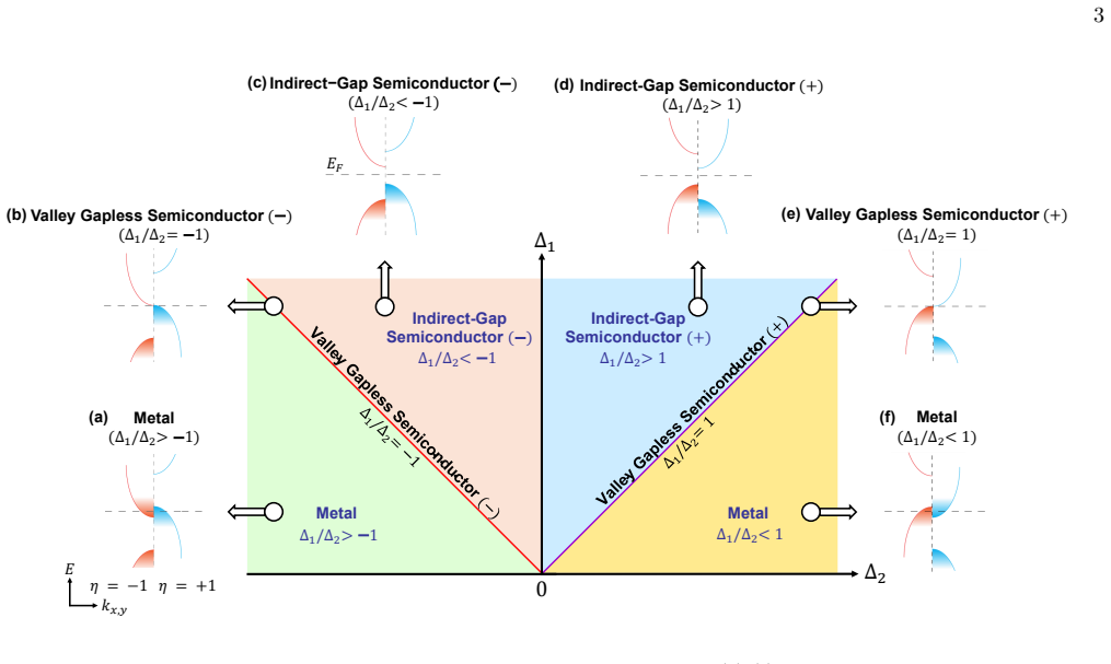
The central object is the two-band Dirac Hamiltonian $H_\eta(k) = \eta\hbar v_{Fx} k_x \tau_x + \hbar v_{Fy} k_y \tau_y + \Delta_1 \tau_z - \eta \Delta_2 \tau_0$, whose two competing terms set the phase. The mechanism is the competition between $\Delta_1$, which opens the same-sign gap in both valleys, and $\Delta_2$, which shifts the Dirac points of the two valleys in opposite energy directions; when the two are equal, the conduction band of one valley meets the valence band of the other at the Fermi level, making the carrier type valley-locked. In the honeycomb lattice the same competition is carried by the Haldane term (time-reversal breaking, $t_H$) and the modified Haldane term (inversion- and time-reversal breaking, $t_{MH}$), with $t_H = t_{MH}$ the VGS condition. The transport calculation then uses wavefunction matching of the Dirac spinors across the lead, gated VGS, and drain regions to obtain the valley-dependent transmission amplitude $t_\eta$ and conductance $G_\eta$.
What would settle it
Measure the valley polarization efficiency $P$ of a gate-controlled VGS device as a function of $U_g$ at low temperature: the central claim predicts a sharp transition from $P = -1$ to $P = +1$ at $U_g = 0$ with $|P| = 1$ on both sides, so a rounded step, plateaus with $|P| < 1$, or a window where both valleys transmit would contradict it. In parallel, a scattering calculation that includes a short-range impurity potential coupling $K$ and $K'$ should show how much intervalley scattering is required to destroy the polarization flip.
Extended reading notes
Core claim
At the heart of the paper is the two-band valley-dependent Dirac Hamiltonian $H_\eta(k) = \eta\hbar v_{Fx} k_x \tau_x + \hbar v_{Fy} k_y \tau_y + \Delta_1 \tau_z - \eta \Delta_2 \tau_0$, where $\Delta_1$ is a Dirac mass that opens an intravalley gap and $\Delta_2$ is a valley-dependent scalar potential that shifts the two Dirac cones in opposite directions. The VGS is the critical line $\Delta_1/\Delta_2 = 1$ (and the mirror line $-1$ for the opposite sign of $\Delta_2$), where the intervalley gap $\Delta_{\mathrm{inter}} = 2(|\Delta_1| - \eta \Delta_2)$ vanishes while the intravalley gap $2|\Delta_1|$ remains nonzero. In the honeycomb realization the same phase appears when $t_H = t_{MH}$, with $t_H$ the Haldane next-nearest-neighbour hopping and $t_{MH}$ the modified Haldane term. The paper's central transport claim is that in a source-VGS-drain junction with a top gate, the valley-dependent transmission $T_\eta$ vanishes inside a gate-voltage window that is valley-dependent, so for $U_g < 0$ only the $\eta = -1$ valley transmits and for $U_g > 0$ only the $\eta = +1$ valley transmits; the valley polarization efficiency $P = (G_+ - G_-)/(G_+ + G_-)$ therefore takes the values $-1$ and $+1$ and flips sharply at $U_g = 0$.
Load-bearing premise
The load-bearing premise is that electrons never scatter between the two valleys while passing through the device, so the valley index is conserved and the two valley conductances can simply be added; the paper supports this with the large momentum separation between valleys and smooth gate potentials, but gives no quantitative disorder estimate, so any appreciable intervalley scattering would wash out the perfect filtering and the sharp polarization flip at zero gate voltage.
Editorial extensions
If this is right
- A single gate voltage can switch a device between fully valley-polarized electron transport and fully valley-polarized hole transport, with the sign of the polarization set by the sign of the gate voltage.
- The VGS phase can be realized in a honeycomb lattice by tuning the modified Haldane hopping to equal the Haldane hopping, a condition already within reach of optical-lattice, photonic-crystal, and topolectrical-circuit realizations.
- In TMDC monolayers with spin-orbit coupling of strength $\lambda_{\mathrm{SOC}}$, the VGS appears in one spin subband when the Semenoff mass vanishes, because both $\Delta_1$ and $\Delta_2$ equal $\lambda_{\mathrm{SOC}}/2$.
- The predicted $P = \pm 1$ plateaus can be probed by helicity-resolved photoluminescence, which the paper identifies as the direct experimental signature.
Reading between the lines
- Editorial inference: the same ratio condition $\Delta_1/\Delta_2 = 1$ suggests that any knob that tunes the two terms independently, such as strain, Floquet driving, or layer stacking, could sweep the system through the VGS line and act as an electrically controllable valve, since the sharp polarization flip appears only at the ratio.
- Editorial inference: the perfect $P = \pm 1$ result is computed from independent valley conductances, so in a real sample short-range disorder or atomically sharp gate edges, which couple valleys, would likely round the plateaus unless the interfaces are made smooth on the lattice scale; quantifying this rounding is a natural next calculation.
- Editorial inference: the sharp sign flip at $U_g = 0$ could be used as a binary valley switch for logic or memory, but the paper does not quantify temperature, noise, or power dissipation, which would determine whether the effect survives in a practical device.
Editorial analysis
A structured set of objections, weighed in public.
Referee Report
Summary. The paper proposes and analyzes the 'valley gapless semiconductor' (VGS), defined in the two-band Dirac Hamiltonian of Eq. (1) by the condition Δ1/Δ2 = ±1, where the Dirac mass Δ1 and a valley-dependent scalar potential Δ2 align the conduction-band edge of one valley with the valence-band edge of the other. The eigenvalues (Eq. (3)) give a clean Δ1–Δ2 phase diagram: indirect-gap semiconductor for |Δ1/Δ2| > 1, metal for |Δ1/Δ2| < 1, and VGS at |Δ1/Δ2| = 1, with valley-polarized carriers in an energy window of width 4|Δ1| centered on the touching point. Section III realizes the VGS in a honeycomb lattice with competing Haldane (tH) and modified Haldane (tMH) hoppings, with the VGS at tMH = tH, and the transport section (Sec. IV) studies a gate-controlled barrier between normal leads, computing valley-resolved transmission, conductance, and polarization P = (G+ − G−)/(G+ + G−) by closed-form mode matching (Appendices A–C). The central claim is that the VGS-based filter produces full valley polarization that flips sharply from P = −1 to P = +1 at Ug = 0, enabling all-electrical valley control.
Significance. The two-band analysis is sound and self-contained: the phase diagram and the VGS condition follow directly from the eigenvalues with no fitting, the honeycomb realization maps onto the continuum model with a single tunable ratio tMH/tH, and the closed-form scattering coefficients in Appendix C make the predicted P = ±1 windows analytically checkable and falsifiable. The conceptual message — that a VGS couples carrier type to valley index and thereby allows electrical switching of valley polarization — is well grounded in the band structure and is of genuine interest for valleytronics, and the paper appropriately distinguishes its proposal from the experimentally observed valley-polarized quantum Hall phase of Pb1−xSnxSe. The main weakness is that the transport section's headline result (the flip at Ug = 0) is tied to an unstated energy reference; once that is fixed, the device prediction is meaningful. The contribution is incremental relative to the authors' earlier VGS proposal (ref. [76]) but supplies a concrete lattice model and a device-level analysis that the earlier work lacked.
major comments (1)
- [Sec. IV (Eqs. (12)–(15)) and Appendix B (Eq. (B2))] The central device claim—full valley polarization with a sharp flip of P at Ug = 0 for the VGS—rests on an energy reference that is never stated. From Z±(x) = E + U(x) + ηΔ2(x) ± Δ1(x) (main text, paragraph containing Eqs. (12)–(13); Appendix B, Eq. (B2)), valley η has a propagating mode in the central region only when |E + Ug + ηΔ2| > Δ1, so the blocking windows are −(E + ηΔ2 + Δ1) < Ug < −(E + ηΔ2 − Δ1). The text instead states them as −(ηΔ2 + Δ1) < Ug < −(ηΔ2 − Δ1), and later quotes P = −1 (+1) for −(Δ2 + Δ1) < Ug < Δ1 − Δ2 (Δ2 − Δ1 < Ug < Δ2 + Δ1), with the flip at Ug = 0; all of these omit E and are correct only for E = 0. Since Sec. IV fixes EF = Ul + E = 1, the choice E = 0 corresponds to the unstated lead potential Ul = 1. With the equally natural choice Ul = 0 (E = EF = 1) and the stated Δ1 = Δ2 = 0.5EF, the same condition gives windows −2 < Ug < −1 (η = + blocked) and −1 < Ug < 0 (η = − blocked), i.e., full polarization of the opposite sign, located at negative Ug, and no fully polarized window for Ug > 0. The headline 'sharp flip at Ug = 0' is therefore a consequence of the chosen zero of energy rather than a gauge-invariant prediction; in general the flip occurs at E + Ug = 0 (equivalently Ug = Ul − EF), the point at which carriers in the barrier switch between electron- and hole-like. This affects the abstract, the mechanism statement in Fig. 3(b) ('For a positive (negative) gate voltage, only the electrons (holes) in the η = +1 (−1) valley are transmitted'), and the conclusion. The revision should state E (or Ul) explicitly, write the windows with E included, and rephrase the flipping condition accordingly.
minor comments (6)
- [Sec. III (Eq. (9) paragraph)] The sentence stating that 'in TMDC monolayers such as MoS2, the VGS is expected in one of the spin subbands' overstates the case: Eq. (9) realizes the VGS only for mS = 0, whereas monolayer MoS2 has a large Semenoff mass (mS ≈ 0.8 eV) that puts Δ1/Δ2 ≈ 1 ± 2mS/λSOC, far from the VGS condition; the claim should be reframed as an engineering scenario (tuning mS toward zero) rather than an expectation for intrinsic MoS2.
- [Sec. IV (Eq. (13) area)] The incident-angle definition is garbled: the text reads θ0 = arcsin(ℏvF ky / E_F^{1/2}), whereas Appendix C (Eq. (C4) and its context) implies sin θ0 = ℏvFy ky / EF; the formula should be corrected.
- [Sec. IV (Eq. (10))] The potential profile U(x) = UlΘ(−x) + UgΘ(dx − x²) + UlΘ(x − d) and the analogous Θ(dx − x²) in Δ1,2(x) use a factor that appears to be a typo for the rectangular-barrier form Θ(x)Θ(d − x); as written the barrier region is not clearly defined and the setup is not reproducible.
- [Sec. IV (intervalley-scattering paragraph)] The assumption that intervalley scattering is negligible is supported only by a qualitative momentum-separation argument and a reference to smoother-potential results in ref. [74]; a quantitative estimate (e.g., the intervalley scattering amplitude or mean free path relative to the valley-selective window width Δ1 and the device length d) would substantially strengthen the device claim.
- [Sec. IV (parameter paragraph)] The statements that the results are 'qualitatively similar for different combinations of the parameters' and 'remain valid under the anisotropic case' are asserted without demonstration; a supporting example or argument would make the robustness claim checkable.
- [Sec. IV (P-window text after Eq. (15))] For the semiconducting phase (Δ2 < Δ1), the stated full-polarization windows −(Δ2+Δ1) < Ug < Δ1−Δ2 (P = −1) and Δ2−Δ1 < Ug < Δ2+Δ1 (P = +1) include the interval |Ug| < Δ1 − Δ2 in which both valleys are blocked (G = 0) and P is ill-defined, as the red dashed line in Fig. 3(e) itself indicates; the windows should be restricted to −(Δ2+Δ1) < Ug < −(Δ1−Δ2) and Δ1−Δ2 < Ug < Δ2+Δ1.
Circularity Check
No significant circularity: the VGS condition and the transport P=±1 response are derived from the model Hamiltonian rather than fitted or defined into existence; the only self-reference is background attribution.
full rationale
The derivation chain is self-contained. The VGS phase condition Δ1/Δ2=1 is obtained algebraically from the eigenvalues E_{η,±}(k)=−ηΔ2±sqrt((ℏvF|k|)^2+Δ1^2) and the definition Δ_inter=2(|Δ1|−ηΔ2); setting Δ_inter=0 gives the VGS condition, so the phase boundary is a consequence of the model, not an input. The honeycomb-lattice realization maps Δ1=tH sinφ and Δ2=tMH sinφ′ and then derives tH=tMH from the same eigenvalue condition; no parameter is fitted to the target phase. The transport calculation is equally direct: valley-dependent transmission Tη, conductance Gη, and polarization P are obtained by wavefunction matching in Appendices A–C, with Z±(x)=E+U(x)+ηΔ2(x)±Δ1(x). The reported blocking windows and the P=+1/−1 response follow from the band structure and the gate potential, not from any fitted quantity. The paper does cite its own earlier VGS concept paper (ref. [76], with overlapping authorship), but that citation is background attribution rather than load-bearing evidence: none of the derivations in Sections II–IV require a theorem or result imported from [76]. The intervalley-scattering-negligible assumption is a stated physical approximation supported by the large momentum separation between valleys and by prior smoother-potential studies; even if it is a weakness, it is an assumption, not a circular reduction. A separate correctness concern is that the blocking windows in Sec. IV omit the incident energy E, so the sharp flip at Ug=0 corresponds to E=0 (i.e., Ul=EF); with Ul=0 the flip would move to Ug=−EF. This is an energy-reference ambiguity and a correctness risk, but it is not circularity because no prediction is being made equal to its own input by construction.
Assumptions & free parameters
free parameters (4)
- Δ1 (Dirac mass in the device) =
0.5 EF
- Δ2/Δ1 ratio =
0.5, 1.0, 1.5 (three phases)
- kF d (central region length) =
20
- tH/t (Haldane hopping in honeycomb band plots) =
0.1
assumptions (5)
- domain assumption Intervalley interaction is negligible, so the Hamiltonian is block-diagonal in valley index.
- domain assumption Interfaces are smooth on the atomic scale, so intervalley scattering at the potential steps is negligible.
- domain assumption The leads are described by the same massless Dirac Hamiltonian with a constant potential Ul, and the incident energy E is measured relative to the Fermi level such that E=0 and EF=Ul.
- domain assumption The TMDC low-energy model of ref. [38] is valid, including Δ1=Δ2 for each spin subband.
- domain assumption The two-band Dirac description captures the band structure near the valley points.
Cite this review
Pith. "Pith review of Valley Gapless Semiconductor: Models and Applications." pith.science (2026). https://pith.science/paper/O7BONGEC
@misc{pith2026250202057,
  author       = {Pith},
  title        = {Pith review of: Valley Gapless Semiconductor: Models and Applications},
  year         = {2026},
  howpublished = {\url{https://pith.science/paper/O7BONGEC}},
  note         = {Machine review of arXiv:2502.02057}
}
read the original abstract
The emerging field of valleytronics harnesses the valley degree of freedom of electrons, akin to how electronic and spintronic devices utilize the charge and spin degrees of freedom of electrons respectively. The engineering of valleytronic devices typically relies on the coupling between valley and other degrees of freedom such as spin, giving rise to valley-spintronics where an external magnetic field manipulates the information stored in valleys. Here, the valley gapless semiconductor is proposed as a potential electrically controlled valleytronic platform because the valley degree of freedom is coupled to the carrier type, i.e., electrons and holes. The valley degree of freedom can be electrically controlled by tuning the carrier type via the device gate voltage. We demonstrate the proposal for realizing a valley gapless semiconductor in the honeycomb lattice with the Haldane and modified Haldane models. The system's valley-carrier coupling is further studied for its transport properties in an all-electrically controlled valley filter device setting. Our work highlights the significance of the valley gapless semiconductor for valleytronic devices.
Figures


Reference graph
Works this paper leans on
- [76]
-
[1]
When ∆ 1 ̸= 0, the Dirac points are destroyed and the band structures illustrated in Fig
(3) For ∆1 = ∆2 = 0, the system is gapless which is known as a Dirac semimetal, supporting two Dirac points lo- calized at the same energy. When ∆ 1 ̸= 0, the Dirac points are destroyed and the band structures illustrated in Fig. 1 reveal an intravalley gap, denoted as ∆ intra, which represents the energy difference between the con- duction and valence ba...
-
[2]
Y. Liu, Y. Gao, S. Zhang, J. He, J. Yu, and Z. Liu, Val- leytronics in transition metal dichalcogenides materials, Nano Res. 12, 2695 (2019)
2019
-
[3]
Zheng, Y.-F
J.-D. Zheng, Y.-F. Zhao, Y.-F. Tan, Z. Guan, N. Zhong, F.-Y. Yue, P.-H. Xiang, and C.-G. Duan, Coupling of ferroelectric and valley properties in 2D materials, J. Appl. Phys. 132, 120902 (2022)
2022
-
[4]
H. Yu, X. Cui, X. Xu, and W. Yao, Valley excitons in two-dimensional semiconductors, Natl. Sci. Rev. 2, 57 (2015)
2015
-
[5]
J. R. Schaibley, H. Yu, G. Clark, P. Rivera, J. S. Ross, K. L. Seyler, W. Yao, and X. Xu, Valleytronics in 2D materials, Nat Rev Mater 1, 16055 (2016)
2016
-
[6]
C. Luo, Z. Huang, H. Qiao, X. Qi, and X. Peng, Val- leytronics in two-dimensional magnetic materials, J. Phys. Mater. 7, 022006 (2024)
2024
-
[7]
X. Xu, W. Yao, D. Xiao, and T. F. Heinz, Spin and pseudospins in layered transition metal dichalcogenides, Nature Phys 10, 343 (2014)
2014
Show all 136 references
-
[8]
Tyulnev, ´A
I. Tyulnev, ´A. Jim´ enez-Gal´ an, J. Poborska, L. Vamos, P. S. J. Russell, F. Tani, O. Smirnova, M. Ivanov, R. E. Silva, and J. Biegert, Valleytronics in bulk MoS2 with a topologic optical field, Nature 628, 746 (2024)
2024
-
[9]
S. Yang, H. Long, W. Chen, B. Sa, Z. Guo, J. Zheng, J. Pei, H. Zhan, and Y. Lu, Valleytronics Meets Strain- tronics: Valley Fine Structure Engineering of 2D Tran- sition Metal Dichalcogenides, Adv. Opt. Mater. 12, 2302900 (2024)
2024
-
[10]
Huang, K
K. Huang, K. Samanta, D.-F. Shao, and E. Y. Tsymbal, Two-Dimensional Nonvolatile Valley Spin Valve, ACS Nano 19, 3448 (2025)
2025
-
[11]
A. R. Nirjhar and S. Ahmed, Magnetic Proximity- Induced Colossal Valley Splitting in WTe 2 for Room Temperature Valleytronics, ACS Appl. Electron. Mater. 7, 2012 (2025)
2025
-
[12]
S.-D. Guo, P. Li, and G. Wang, First-principles calcu- lations study of valley polarization in antiferromagnetic bilayer systems, Phys. Rev. B 111, L140404 (2025)
2025
-
[13]
Jiang, Y
H. Jiang, Y. Zhang, L. An, Q. Tan, X. Dai, Y. Chen, W. Chen, H. Cai, J. Fu, J. Z´ u˜ niga-P´ erez,et al., Chi- ral light detection with centrosymmetric-metamaterial- assisted valleytronics, Nat. Mater. , 1 (2025)
2025
-
[14]
Shen, J.-D
Y.-H. Shen, J.-D. Zheng, W.-Y. Tong, Z.-Q. Bao, X.-G. Wan, and C.-G. Duan, Twist-induced quantum valley Hall states in bilayer germanene, Phys. Rev. B 111, 075421 (2025)
2025
-
[15]
A. M. Shirai, Y. Murotani, T. Fujimoto, N. Kanda, J. Yoshinobu, and R. Matsunaga, Valley polarization dynamics of photoinjected carriers at the band edge in room-temperature silicon studied by terahertz po- larimetry, Phys. Rev. B 111, L121201 (2025)
2025
-
[16]
R. Wang, K. Chang, W. Duan, Y. Xu, and P. Tang, Twist-Angle-Dependent Valley Polarization of In- tralayer Moir´ e Excitons in van der Waals Superlattices, 10 Phys. Rev. Lett. 134, 026904 (2025)
2025
-
[17]
Herrmann, S
P. Herrmann, S. Klimmer, T. Lettau, T. Weickhardt, A. Papavasileiou, K. Mosina, Z. Sofer, I. Paradisanos, D. Kartashov, J. Wilhelm, et al., Nonlinear valley selec- tion rules and all-optical probe of broken time-reversal symmetry in monolayer WSe 2, Nat. Photon. 19, 300 (2025)
2025
-
[18]
Jiang, L.-Y
X.-C. Jiang, L.-Y. Qiao, and Y.-Z. Zhang, Anomalous valley Hall effect in monolayer chromium-based triple-Q magnets, Phys. Rev. B 111, L140416 (2025)
2025
-
[19]
Zhang, J
W. Zhang, J. Zhou, and S. Cheng, Valley transport in breathing kagome lattices with chiral spin textures, Phys. Rev. B 111, 165307 (2025)
2025
-
[20]
Gunawan, Y
O. Gunawan, Y. P. Shkolnikov, K. Vakili, T. Gokmen, E. P. De Poortere, and M. Shayegan, Valley Susceptibil- ity of an Interacting Two-Dimensional Electron System, Phys. Rev. Lett. 97, 186404 (2006)
2006
-
[21]
ˇZuti´ c, J
I. ˇZuti´ c, J. Fabian, and S. Das Sarma, Spintronics: Fun- damentals and applications, Rev. Mod. Phys. 76, 323 (2004)
2004
-
[22]
M. A. Mueed, M. S. Hossain, I. Jo, L. N. Pfeiffer, K. W. West, K. W. Baldwin, and M. Shayegan, Realization of a Valley Superlattice, Phys. Rev. Lett. 121, 036802 (2018)
2018
-
[23]
Gokmen, M
T. Gokmen, M. Padmanabhan, O. Gunawan, Y. P. Shkolnikov, K. Vakili, E. P. De Poortere, and M. Shayegan, Parallel magnetic-field tuning of valley splitting in AlAs two-dimensional electrons, Phys. Rev. B 78, 233306 (2008)
2008
-
[24]
Shen, W.-Y
X.-W. Shen, W.-Y. Tong, S.-J. Gong, and C.-G. Duan, Electrically tunable polarizer based on 2D orthorhombic ferrovalley materials, 2D Mater. 5, 011001 (2017)
2017
-
[25]
Tong, S.-J
W.-Y. Tong, S.-J. Gong, X. Wan, and C.-G. Duan, Con- cepts of ferrovalley material and anomalous valley Hall effect, Nat Commun 7, 13612 (2016)
2016
-
[26]
Hu, W.-Y
H. Hu, W.-Y. Tong, Y.-H. Shen, X. Wan, and C.-G. Duan, Concepts of the half-valley-metal and quantum anomalous valley Hall effect, npj Comput Mater 6, 129 (2020)
2020
-
[27]
Y. Lai, Z. Song, Y. Wan, M. Xue, C. Wang, Y. Ye, L. Dai, Z. Zhang, W. Yang, H. Du, et al. , Two- dimensional ferromagnetism and driven ferroelectricity in van der Waals CuCrP2S6, Nanoscale 11, 5163 (2019)
2019
-
[28]
T. Cao, G. Wang, W. Han, H. Ye, C. Zhu, J. Shi, Q. Niu, P. Tan, E. Wang, B. Liu, et al., Valley-selective circu- lar dichroism of monolayer molybdenum disulphide, Nat Commun 3, 887 (2012)
2012
-
[29]
Z. Wan, W. Zhou, G. Zheng, H. Duan, Y. Chen, and F. Ouyang, Tuning the Magnetization Direction and Valley Splitting of Monolayer Ferrovalley CrISe: Impli- cations for Spintronics and Valleytronics Devices, ACS Appl. Nano Mater. 8, 2466 (2025)
2025
-
[30]
A. M. Jones, H. Yu, N. J. Ghimire, S. Wu, G. Aivazian, J. S. Ross, B. Zhao, J. Yan, D. G. Mandrus, D. Xiao, et al., Optical generation of excitonic valley coherence in monolayer WSe2, Nature Nanotech 8, 634 (2013)
2013
-
[31]
H. Zeng, J. Dai, W. Yao, D. Xiao, and X. Cui, Valley polarization in MoS 2 monolayers by optical pumping, Nature Nanotech 7, 490 (2012)
2012
-
[32]
Aivazian, Z
G. Aivazian, Z. Gong, A. M. Jones, R.-L. Chu, J. Yan, D. G. Mandrus, C. Zhang, D. Cobden, W. Yao, and X. Xu, Magnetic control of valley pseudospin in mono- layer WSe2, Nature Phys 11, 148 (2015)
2015
-
[33]
Suzuki, M
R. Suzuki, M. Sakano, Y. Zhang, R. Akashi, D. Morikawa, A. Harasawa, K. Yaji, K. Kuroda, K. Miyamoto, T. Okuda, et al., Valley-dependent spin polarization in bulk MoS 2 with broken inversion sym- metry, Nature Nanotech 9, 611 (2014)
2014
-
[34]
Zhong, K
D. Zhong, K. L. Seyler, X. Linpeng, R. Cheng, N. Sivadas, B. Huang, E. Schmidgall, T. Taniguchi, K. Watanabe, M. A. McGuire, W. Yao, D. Xiao, K.- M. C. Fu, and X. Xu, Van der Waals engineering of ferromagnetic semiconductor heterostructures for spin and valleytronics, Sci. Adv...
2017
-
[35]
Z. Wang, J. Shan, and K. F. Mak, Valley-and spin- polarized Landau levels in monolayer WSe 2, Nature Nanotech 12, 144 (2017)
2017
-
[36]
Z. Wu, B. T. Zhou, X. Cai, P. Cheung, G.-B. Liu, M. Huang, J. Lin, T. Han, L. An, Y. Wang, et al., In- trinsic valley Hall transport in atomically thin MoS 2, Nat Commun 10, 611 (2019)
2019
-
[37]
P. Dey, L. Yang, C. Robert, G. Wang, B. Urbaszek, X. Marie, and S. A. Crooker, Gate-Controlled Spin- Valley Locking of Resident Carriers in WSe 2 Monolay- ers, Phys. Rev. Lett. 119, 137401 (2017)
2017
-
[38]
Xiao, G.-B
D. Xiao, G.-B. Liu, W. Feng, X. Xu, and W. Yao, Cou- pled Spin and Valley Physics in Monolayers of MoS 2 and Other Group-VI Dichalcogenides, Phys. Rev. Lett. 108, 196802 (2012)
2012
-
[39]
L. Li, L. Shao, X. Liu, A. Gao, H. Wang, B. Zheng, G. Hou, K. Shehzad, L. Yu, F. Miao, et al., Room- temperature valleytronic transistor, Nat. Nanotechnol. 15, 743 (2020)
2020
-
[40]
Gong, G.-B
Z. Gong, G.-B. Liu, H. Yu, D. Xiao, X. Cui, X. Xu, and W. Yao, Magnetoelectric effects and valley-controlled spin quantum gates in transition metal dichalcogenide bilayers, Nat Commun 4, 2053 (2013)
2013
-
[41]
R. Xu, Z. Zhang, J. Liang, and H. Zhu, Valleytronics: Fundamental Challenges and Materials Beyond Transi- tion Metal Chalcogenides, Small , 2402139 (2024)
2024
-
[42]
A. M. Jones, H. Yu, J. S. Ross, P. Klement, N. J. Ghimire, J. Yan, D. G. Mandrus, W. Yao, and X. Xu, Spin–layer locking effects in optical orientation of exci- ton spin in bilayer WSe 2, Nature Phys 10, 130 (2014)
2014
-
[43]
S. Wu, J. S. Ross, G.-B. Liu, G. Aivazian, A. Jones, Z. Fei, W. Zhu, D. Xiao, W. Yao, D. Cobden, et al., Electrical tuning of valley magnetic moment through symmetry control in bilayer MoS 2, Nature Phys 9, 149 (2013)
2013
-
[44]
Shimazaki, M
Y. Shimazaki, M. Yamamoto, I. V. Borzenets, K. Watanabe, T. Taniguchi, and S. Tarucha, Generation and detection of pure valley current by electrically in- duced Berry curvature in bilayer graphene, Nature Phys 11, 1032 (2015)
2015
-
[45]
M. Sui, G. Chen, L. Ma, W.-Y. Shan, D. Tian, K. Watanabe, T. Taniguchi, X. Jin, W. Yao, D. Xiao, et al., Gate-tunable topological valley transport in bi- layer graphene, Nature Phys 11, 1027 (2015)
2015
-
[46]
Scuri, T
G. Scuri, T. I. Andersen, Y. Zhou, D. S. Wild, J. Sung, R. J. Gelly, D. B´ erub´ e, H. Heo, L. Shao, A. Y. Joe, A. M. Mier Valdivia, T. Taniguchi, K. Watanabe, M. Lonˇ car, P. Kim, M. D. Lukin, and H. Park, Electrically Tun- able Valley Dynamics in Twisted WSe2/WSe2 Bilayers, ...
2020
-
[47]
J. Lee, K. F. Mak, and J. Shan, Electrical control of the valley Hall effect in bilayer MoS 2 transistors, Nature Nanotech 11, 421 (2016)
2016
-
[48]
Zhang, X
T. Zhang, X. Xu, B. Huang, Y. Dai, L. Kou, and Y. Ma, Layer-polarized anomalous Hall effects in valleytronic van der Waals bilayers, Mater. Horiz. 10, 483 (2023). 11
2023
-
[49]
Z.-M. Yu, S. Guan, X.-L. Sheng, W. Gao, and S. A. Yang, Valley-Layer Coupling: A New Design Principle for Valleytronics, Phys. Rev. Lett. 124, 037701 (2020)
2020
-
[50]
S. V. Morozov, K. S. Novoselov, M. I. Katsnelson, F. Schedin, L. A. Ponomarenko, D. Jiang, and A. K. Geim, Strong Suppression of Weak Localization in Graphene, Phys. Rev. Lett. 97, 016801 (2006)
2006
-
[51]
McCann, K
E. McCann, K. Kechedzhi, V. I. Fal’ko, H. Suzuura, T. Ando, and B. L. Altshuler, Weak-Localization Mag- netoresistance and Valley Symmetry in Graphene, Phys. Rev. Lett. 97, 146805 (2006)
2006
-
[52]
Y. S. Ang, S. A. Yang, C. Zhang, Z. Ma, and L. K. Ang, Valleytronics in merging Dirac cones: All-electric- controlled valley filter, valve, and universal reversible logic gate, Phys. Rev. B 96, 245410 (2017)
2017
-
[53]
A. F. Morpurgo and F. Guinea, Intervalley Scatter- ing, Long-Range Disorder, and Effective Time-Reversal Symmetry Breaking in Graphene, Phys. Rev. Lett. 97, 196804 (2006)
2006
-
[54]
J. Xin, Y. Tang, Y. Liu, X. Zhao, H. Pan, and T. Zhu, Valleytronics in thermoelectric materials, npj Quant Mater 3, 9 (2018)
2018
-
[55]
J. Chen, Y. Zhou, J. Yan, J. Liu, L. Xu, J. Wang, T. Wan, Y. He, W. Zhang, and Y. Chai, Room- temperature valley transistors for low-power neuromor- phic computing, Nat Commun 13, 7758 (2022)
2022
-
[56]
C. W. J. Beenakker, N. V. Gnezdilov, E. Dresselhaus, V. P. Ostroukh, Y. Herasymenko, i. d. I. Adagideli, and J. Tworzyd lo, Valley switch in a graphene super- lattice due to pseudo-Andreev reflection, Phys. Rev. B 97, 241403 (2018)
2018
-
[57]
Y.-M. Xie, D. K. Efetov, and K. T. Law, φ0-Josephson junction in twisted bilayer graphene induced by a valley- polarized state, Phys. Rev. Res. 5, 023029 (2023)
2023
-
[58]
The key challenge to designing valleytronic devices in- volves generating and manipulating valley-polarized car- riers
and other novel devices [59–65]. The key challenge to designing valleytronic devices in- volves generating and manipulating valley-polarized car- riers. The degeneracy of the two valleys, protected by both the time-reversal and inversion symmetries, lim- its their direct appli...
2025 arXiv
-
[59]
J. J. Wang, S. Liu, J. Wang, and J.-F. Liu, Valley su- percurrent in the Kekul´ e graphene superlattice hetero- junction, Phys. Rev. B 101, 245428 (2020)
2020
-
[60]
X. Wu, H. Meng, F. Kong, H. Zhang, Y. Bai, and N. Xu, Tunable nonlocal valley-entangled Cooper pair splitter realized in bilayer-graphene van der Waals spin valves, Phys. Rev. B 101, 125406 (2020)
2020
-
[61]
X. Chen, L. Zhang, and H. Guo, Valley caloritronics and its realization by graphene nanoribbons, Phys. Rev. B 92, 155427 (2015)
2015
-
[62]
X.-T. An, J. Xiao, M. W.-Y. Tu, H. Yu, V. I. Fal’ko, and W. Yao, Realization of Valley and Spin Pumps by Scattering at Nonmagnetic Disorders, Phys. Rev. Lett. 118, 096602 (2017)
2017
-
[63]
Z. Wu, F. Zhai, F. M. Peeters, H. Q. Xu, and K. Chang, Valley-Dependent Brewster Angles and Goos-H¨ anchen Effect in Strained Graphene, Phys. Rev. Lett. 106, 176802 (2011)
2011
-
[64]
X. Qiu, Q. Lv, and Z. Cao, A high-quality spin and val- ley beam splitter in WSe 2 tunnelling junction through the Goos–H¨ anchen shift, J. Phys.: Condens. Matter31, 225303 (2019)
2019
-
[65]
R. Liu, Y. Zhang, Y. Zhou, J. Nie, L. Li, and Y. Zhang, Polarization-driven high Rabi frequency of piezotronic valley transistors, Nano Energy 113, 108550 (2023)
2023
-
[66]
S. Lai, Z. Zhang, N. Wang, A. Rasmita, Y. Deng, Z. Liu, and W.-b. Gao, Dual-Gate All-Electrical Valleytronic Transistors, Nano Lett. 23, 192 (2023)
2023
-
[67]
K. Shao, H. Geng, E. Liu, J. L. Lado, W. Chen, and D. Y. Xing, Non-Hermitian Moir´ e Valley Filter, Phys. Rev. Lett. 132, 156301 (2024)
2024
-
[68]
D. Xiao, W. Yao, and Q. Niu, Valley-Contrasting Physics in Graphene: Magnetic Moment and Topologi- cal Transport, Phys. Rev. Lett. 99, 236809 (2007)
2007
-
[69]
K. Das, K. Ghorai, D. Culcer, and A. Agarwal, Non- linear Valley Hall Effect, Phys. Rev. Lett. 132, 096302 (2024)
2024
-
[70]
Ghadimi, C
R. Ghadimi, C. Mondal, S. Kim, and B.-J. Yang, Quan- tum Valley Hall Effect without Berry Curvature, Phys. Rev. Lett. 133, 196603 (2024)
2024
-
[71]
Zhang, D.-F
S.-H. Zhang, D.-F. Shao, Z.-A. Wang, J. Yang, W. Yang, and E. Y. Tsymbal, Tunneling Valley Hall Effect Driven by Tilted Dirac Fermions, Phys. Rev. Lett. 131, 246301 (2023)
2023
-
[72]
J. Zhou, Q. Sun, and P. Jena, Valley-Polarized Quan- tum Anomalous Hall Effect in Ferrimagnetic Honey- comb Lattices, Phys. Rev. Lett. 119, 046403 (2017)
2017
-
[73]
H. Pan, Z. Li, C.-C. Liu, G. Zhu, Z. Qiao, and Y. Yao, Valley-Polarized Quantum Anomalous Hall Effect in Sil- icene, Phys. Rev. Lett. 112, 106802 (2014)
2014
-
[74]
H. Pan, X. Li, F. Zhang, and S. A. Yang, Perfect valley filter in a topological domain wall, Phys. Rev. B 92, 041404 (2015)
2015
-
[75]
H. Pan, X. Li, H. Jiang, Y. Yao, and S. A. Yang, Valley- polarized quantum anomalous Hall phase and disorder- induced valley-filtered chiral edge channels, Phys. Rev. B 91, 045404 (2015)
2015
-
[77]
X. L. Wang, Proposal for a New Class of Materials: Spin Gapless Semiconductors, Phys. Rev. Lett. 100, 156404 (2008)
2008
-
[78]
Guo, Y.-L
S.-D. Guo, Y.-L. Tao, G. Wang, S. Chen, D. Huang, and Y. S. Ang, Proposal for valleytronic materials: Fer- rovalley metal and valley gapless semiconductor, Front. Phys. 19, 23302 (2024)
2024
-
[79]
Krizman, J
G. Krizman, J. Bermejo-Ortiz, T. Zakusylo, M. Ha- jlaoui, T. Takashiro, M. Rosmus, N. Olszowska, J. J. Ko lodziej, G. Bauer, Y. Guldner, G. Springholz, and L.- A. de Vaulchier, Valley-Polarized Quantum Hall Phase in a Strain-Controlled Dirac System, Phys. Rev. Lett. 132, 166601 (2024)
2024
-
[80]
F. D. M. Haldane, Model for a Quantum Hall Effect without Landau Levels: Condensed-Matter Realization of the ”Parity Anomaly”, Phys. Rev. Lett. 61, 2015 (1988)
1988
-
[81]
Colom´ es and M
E. Colom´ es and M. Franz, Antichiral Edge States in a Modified Haldane Nanoribbon, Phys. Rev. Lett. 120, 086603 (2018)
2018
-
[82]
Qi, Y.-S
X.-L. Qi, Y.-S. Wu, and S.-C. Zhang, Topological quan- tization of the spin Hall effect in two-dimensional para- magnetic semiconductors, Phys. Rev. B 74, 085308 (2006)
2006
-
[83]
Ezawa, Spin valleytronics in silicene: Quantum spin Hall–quantum anomalous Hall insulators and single- valley semimetals, Phys
M. Ezawa, Spin valleytronics in silicene: Quantum spin Hall–quantum anomalous Hall insulators and single- valley semimetals, Phys. Rev. B 87, 155415 (2013)
2013
-
[84]
Jotzu, M
G. Jotzu, M. Messer, R. Desbuquois, M. Lebrat, T. Uehlinger, D. Greif, and T. Esslinger, Experimen- tal realization of the topological Haldane model with ultracold fermions, Nature 515, 237 (2014)
2014
-
[85]
J. W. McIver, B. Schulte, F.-U. Stein, T. Matsuyama, G. Jotzu, G. Meier, and A. Cavalleri, Light-induced anomalous Hall effect in graphene, Nat. Phys. 16, 38 (2020)
2020
-
[86]
T. Li, S. Jiang, B. Shen, Y. Zhang, L. Li, Z. Tao, T. Devakul, K. Watanabe, T. Taniguchi, L. Fu, et al., Quantum anomalous Hall effect from intertwined moir´ e 12 bands, Nature 600, 641 (2021)
2021
-
[87]
Zhou, G.-G
P. Zhou, G.-G. Liu, Y. Yang, Y.-H. Hu, S. Ma, H. Xue, Q. Wang, L. Deng, and B. Zhang, Observation of Pho- tonic Antichiral Edge States, Phys. Rev. Lett. 125, 263603 (2020)
2020
-
[88]
Y. Yang, D. Zhu, Z. Hang, and Y. Chong, Observation of antichiral edge states in a circuit lattice, Sci. China Phys. Mech. Astron. 64, 1 (2021)
2021
-
[89]
M. Vila, N. T. Hung, S. Roche, and R. Saito, Tunable circular dichroism and valley polarization in the modi- fied Haldane model, Phys. Rev. B 99, 161404 (2019)
2019
-
[90]
Ezawa, Photoinduced Topological Phase Transition and a Single Dirac-Cone State in Silicene, Phys
M. Ezawa, Photoinduced Topological Phase Transition and a Single Dirac-Cone State in Silicene, Phys. Rev. Lett. 110, 026603 (2013)
2013
-
[91]
W. Zhao, K. Kang, Y. Zhang, P. Kn¨ uppel, Z. Tao, L. Li, C. L. Tschirhart, E. Redekop, K. Watanabe, T. Taniguchi, et al., Realization of the Haldane Chern insulator in a moir´ e lattice, Nat. Phys.20, 275 (2024)
2024
-
[92]
Mitra, ´A
S. Mitra, ´A. Jim´ enez-Gal´ an, M. Aulich, M. Neuhaus, R. E. Silva, V. Pervak, M. F. Kling, and S. Biswas, Light-wave-controlled Haldane model in monolayer hexagonal boron nitride, Nature , 1 (2024)
2024
-
[93]
Oka and H
T. Oka and H. Aoki, Photovoltaic Hall effect in graphene, Phys. Rev. B 79, 081406 (2009)
2009
-
[94]
Hofmann, T
T. Hofmann, T. Helbig, C. H. Lee, M. Greiter, and R. Thomale, Chiral Voltage Propagation and Calibra- tion in a Topolectrical Chern Circuit, Phys. Rev. Lett. 122, 247702 (2019)
2019
-
[95]
Liu, F.-L
J.-W. Liu, F.-L. Shi, K. Shen, X.-D. Chen, K. Chen, W.- J. Chen, and J.-W. Dong, Antichiral surface states in time-reversal-invariant photonic semimetals, Nat Com- mun 14, 2027 (2023)
2023
-
[96]
X. Xi, B. Yan, L. Yang, Y. Meng, Z.-X. Zhu, J.-M. Chen, Z. Wang, P. Zhou, P. P. Shum, Y. Yang, et al., Topological antichiral surface states in a magnetic Weyl photonic crystal, Nat Commun 14, 1991 (2023)
2023
-
[97]
H. Yuan, M. S. Bahramy, K. Morimoto, S. Wu, K. No- mura, B.-J. Yang, H. Shimotani, R. Suzuki, M. Toh, C. Kloc, et al., Zeeman-type spin splitting controlled by an electric field, Nature Phys 9, 563 (2013)
2013
-
[98]
B. Yang, E. Molina, J. Kim, D. Barroso, M. Lohmann, Y. Liu, Y. Xu, R. Wu, L. Bartels, K. Watan- abe, T. Taniguchi, and J. Shi, Effect of Distance on Photoluminescence Quenching and Proximity-Induced Spin–Orbit Coupling in Graphene/WSe 2 Heterostruc- tures, Nano Lett. 18, 3580 (2018)
2018
-
[99]
Cheiwchanchamnangij, W
T. Cheiwchanchamnangij, W. R. L. Lambrecht, Y. Song, and H. Dery, Strain effects on the spin-orbit- induced band structure splittings in monolayer MoS 2 and graphene, Phys. Rev. B 88, 155404 (2013)
2013
-
[100]
Fujita, M
T. Fujita, M. B. A. Jalil, and S. G. Tan, Valley filter in strain engineered graphene, Appl. Phys. Lett. 97, 043508 (2010)
2010
-
[101]
M. I. Katsnelson, K. S. Novoselov, and A. K. Geim, Chiral tunnelling and the Klein paradox in graphene, Nature Phys 2, 620 (2006)
2006
-
[102]
Ozawa, A
T. Ozawa, A. Amo, J. Bloch, and I. Carusotto, Klein tunneling in driven-dissipative photonic graphene, Phys. Rev. A 96, 013813 (2017)
2017
-
[103]
C. W. J. Beenakker, Colloquium: Andreev reflection and Klein tunneling in graphene, Rev. Mod. Phys. 80, 1337 (2008)
2008
-
[104]
A. H. Castro Neto, F. Guinea, N. M. R. Peres, K. S. Novoselov, and A. K. Geim, The electronic properties of graphene, Rev. Mod. Phys. 81, 109 (2009)
2009
-
[105]
P. E. Allain and J.-N. Fuchs, Klein tunneling in graphene: optics with massless electrons, Eur. Phys. J. B 83, 301 (2011)
2011
-
[106]
A. R. Myers, D. B. Sulas-Kern, R. Fei, D. Ghoshal, M. A. Hermosilla-Palacios, and J. L. Blackburn, Quanti- fying carrier density in monolayer MoS2 by optical spec- troscopy, J. Chem. Phys. 161, 044706 (2024)
2024
-
[107]
Y. Yin, Z. Cheng, L. Wang, K. Jin, and W. Wang, Graphene, a material for high temperature devices– intrinsic carrier density, carrier drift velocity and lattice energy, Sci Rep 4, 5758 (2014)
2014
-
[108]
Friesen, S
M. Friesen, S. Chutia, C. Tahan, and S. N. Coppersmith, Valley splitting theory of SiGe /Si/SiGe quantum wells, Phys. Rev. B 75, 115318 (2007)
2007
-
[109]
N. H. Shon and T. Ando, Quantum transport in two- dimensional graphite system, J. Phys. Soc. Jpn. 67, 2421 (1998)
1998
-
[110]
K. F. Mak, K. He, J. Shan, and T. F. Heinz, Control of valley polarization in monolayer MoS 2 by optical helic- ity, Nature Nanotech 7, 494 (2012)
2012
-
[111]
J. M. Koh, T. Tai, and C. H. Lee, Simulation of Interaction-Induced Chiral Topological Dynamics on a Digital Quantum Computer, Phys. Rev. Lett. 129, 140502 (2022)
2022
-
[112]
J. Wang, S. Valligatla, Y. Yin, L. Schwarz, M. Medina- S´ anchez, S. Baunack, C. H. Lee, R. Thomale, S. Li, V. M. Fomin, et al., Experimental observation of Berry phases in optical M¨ obius-strip microcavities, Nat. Pho- ton. 17, 120 (2023)
2023
-
[113]
S. A. Vitale, D. Nezich, J. O. Varghese, P. Kim, N. Gedik, P. Jarillo-Herrero, D. Xiao, and M. Roth- schild, Valleytronics: Opportunities, Challenges, and Paths Forward, Small 14, 1801483 (2018)
2018
-
[114]
C. H. Lee and X.-L. Qi, Lattice construction of pseu- dopotential Hamiltonians for fractional Chern insula- tors, Phys. Rev. B 90, 085103 (2014)
2014
-
[115]
T. D. Stanescu, V. Galitski, and S. Das Sarma, Topo- logical states in two-dimensional optical lattices, Phys. Rev. A 82, 013608 (2010)
2010
-
[116]
Raoux, M
A. Raoux, M. Morigi, J.-N. Fuchs, F. Pi´ echon, and G. Montambaux, From Dia- to Paramagnetic Orbital Susceptibility of Massless Fermions, Phys. Rev. Lett. 112, 026402 (2014)
2014
-
[117]
K. W. Lee, P.-H. Fu, and Y. S. Ang, Interplay between Haldane and modified Haldane models in α−T3 lattice: Band structures, phase diagrams, and edge states, Phys. Rev. B 109, 235105 (2024)
2024
-
[118]
Vidal, R
J. Vidal, R. Mosseri, and B. Dou¸ cot, Aharonov-Bohm Cages in Two-Dimensional Structures, Phys. Rev. Lett. 81, 5888 (1998)
1998
-
[119]
Vidal, P
J. Vidal, P. Butaud, B. Dou¸ cot, and R. Mosseri, Dis- order and interactions in Aharonov-Bohm cages, Phys. Rev. B 64, 155306 (2001)
2001
-
[120]
Oka and S
T. Oka and S. Kitamura, Floquet Engineering of Quan- tum Materials, Annu. Rev. Condens. Matter Phys. 10, 387 (2019)
2019
-
[121]
K. W. Lee, M. J. A. Calderon, X.-L. Yu, C. H. Lee, Y. S. Ang, and P.-H. Fu, Floquet engineering of topological phase transitions in a quantum spin Hall α−T3 system, Phys. Rev. B 111, 045406 (2025). 13
2025
-
[122]
Goldman and J
N. Goldman and J. Dalibard, Periodically Driven Quan- tum Systems: Effective Hamiltonians and Engineered Gauge Fields, Phys. Rev. X 4, 031027 (2014)
2014
-
[123]
Rahav, I
S. Rahav, I. Gilary, and S. Fishman, Effective Hamilto- nians for periodically driven systems, Phys. Rev. A 68, 013820 (2003)
2003
-
[124]
Plekhanov, G
K. Plekhanov, G. Roux, and K. Le Hur, Floquet engi- neering of Haldane Chern insulators and chiral bosonic phase transitions, Phys. Rev. B 95, 045102 (2017)
2017
-
[125]
C. H. Lee, W. W. Ho, B. Yang, J. Gong, and Z. Papi´ c, Floquet Mechanism for Non-Abelian Fractional Quan- tum Hall States, Phys. Rev. Lett. 121, 237401 (2018)
2018
-
[126]
F. Qin, C. H. Lee, and R. Chen, Light-induced phase crossovers in a quantum spin Hall system, Phys. Rev. B 106, 235405 (2022)
2022
-
[127]
F. Qin, R. Chen, and C. H. Lee, Light-enhanced non- linear Hall effect, Commun Phys 7, 368 (2024)
2024
-
[128]
Stegmaier, A
A. Stegmaier, A. Fritzsche, R. Sorbello, M. Greiter, H. Brand, C. Barko, M. Hofer, U. Schwingenschl¨ ogl, R. Moessner, C. H. Lee, A. Szameit, A. Alu, T. Kießling, and R. Thomale, Topological Edge State Nucleation in Frequency Space and its Realization with Floquet Elec- trical...
2024 arXiv
-
[129]
Li, P.-H
R. Li, P.-H. Fu, J.-F. Liu, and J. Wang, Armchair edge states in shear-strained graphene: Magnetic properties and quantum valley Hall edge states, Phys. Rev. B 109, 045403 (2024)
2024
-
[130]
S.-D. Guo, Y. Liu, J. Yu, and C.-C. Liu, Valley polar- ization in twisted altermagnetism, Phys. Rev. B 110, L220402 (2024)
2024
-
[131]
C.-C. Liu, H. Jiang, and Y. Yao, Low-energy effec- tive Hamiltonian involving spin-orbit coupling in sil- icene and two-dimensional germanium and tin, Phys. Rev. B 84, 195430 (2011)
2011
-
[132]
L¨ u, Y.-C
X.-L. L¨ u, Y.-C. Zhang, P.-H. Fu, and J.-F. Liu, Phase diagrams and topological mixed edge states in silicene with intrinsic and extrinsic Rashba effects, Phys. Rev. Res. 6, 043108 (2024)
2024
-
[133]
S.-Q. Lin, H. Tan, P.-H. Fu, and J.-F. Liu, Interaction- driven Chern insulating phases in the α-T3 lattice with Rashba spin-orbit coupling, iScience 26 (2023)
2023
-
[134]
Dai, P.-H
X. Dai, P.-H. Fu, Y. S. Ang, and Q. Chen, Two- dimensional Weyl nodal-line semimetal and antihelical edge states in a modified Kane-Mele model, Phys. Rev. B 110, 195409 (2024)
2024
-
[135]
P. A. M. Dirac, The quantum theory of the electron, Proc. R. Soc. Lond. A 117, 610 (1928)
1928
-
[136]
P. A. M. Dirac, The Principles of Quantum Mechanics (Clarendon Press, Oxford, 1930)
1930
Reviewed August 9, 2026 · model on record in the stance chip above.
Discussion (0). Continue with ORCID to comment.