A High Input Impedance Chopper Stabilized Amplifier Based On Charge Conservation
Pith reviewed 2026-06-27 05:47 UTC · model grok-4.3
The pith
Differential capacitor flipping makes chopper amplifier input impedance purely capacitive and independent of chopping frequency.
A machine-rendered reading of the paper's core claim, the machinery that carries it, and where it could break.
Core claim
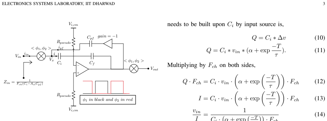
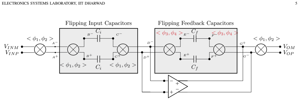
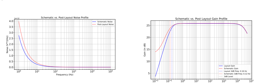
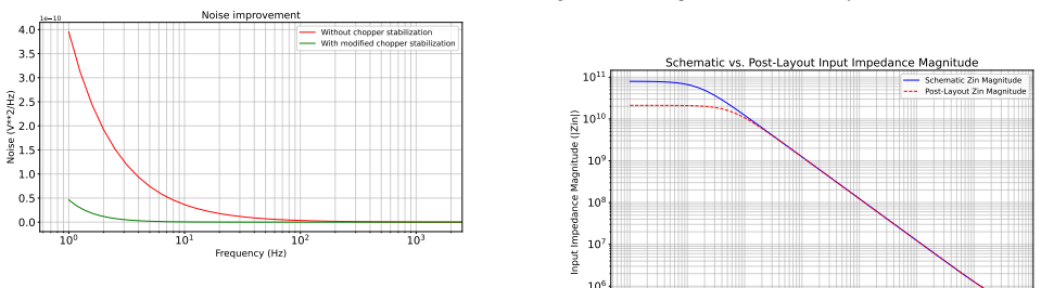
The differential capacitor flipping technique for chopper based CCIA prevents discharge and recharge of Ci's in every cycle by reconfiguring the capacitor positions while preserving the chopping operation. This ideally results in a purely capacitive Zin which is independent of Fch. The circuit implemented in TSMC 65 nm CMOS technology node features Zin of 21 GOhms at DC.
What carries the argument
Differential capacitor flipping technique, which reconfigures input capacitor positions to conserve charge while preserving chopping.
If this is right
- The amplifier can interface directly with sensors having output impedances of several megaohms without loading effects.
- Higher chopping frequencies become usable for flicker noise reduction because they no longer reduce input impedance.
- ECG acquisition with dry electrodes becomes feasible at low power without external buffering.
- The same charge-conservation approach applies to other capacitively coupled chopper amplifiers in CMOS.
Where Pith is reading between the lines
- The method could support multi-channel biopotential recording arrays where sensor loading must stay minimal across channels.
- If charge conservation holds across process corners, the technique may reduce the need for large on-chip input capacitors.
- Extension to other sensor types with high output impedance, such as certain chemical or pressure sensors, appears direct.
Load-bearing premise
Reconfiguring the capacitor positions maintains the chopping operation and achieves charge conservation without introducing additional charge injection, noise, or offset that would affect performance or the claimed independence from Fch.
What would settle it
A plot of measured input impedance versus chopping frequency that remains flat rather than falling inversely with frequency.
Figures


read the original abstract
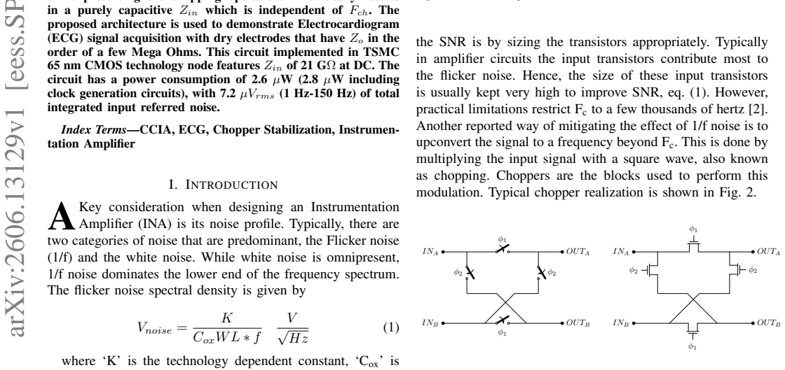
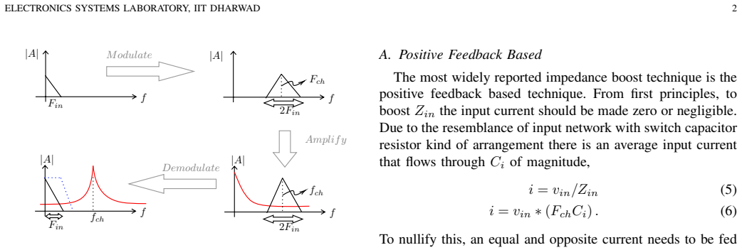
Chopper stabilized amplifiers are popularly used for realizing amplifiers with low offset and for rejecting flicker noise. One of the main limitations of these amplifiers is the low Input Impedance (Zin) produced by the switch capacitor input network. Zin here is resistive due to the switch capacitor action and is inversely proportional to the product of Chopping frequency (Fch) and Input Capacitance (Ci). Since Fch should be greater than the flicker noise corner frequency, this results in a low Zin. When interfacing sensors with high Sensor Output Impedance (Zo), chopper stabilized amplifiers load the sensors resulting in reduced sensitivity. This paper presents a novel input impedance boosting technique - Differential capacitor flipping technique for chopper based Capacitively Coupled Instrumentation Amplifier (CCIA), which prevents discharge and recharge of Ci's in every cycle by reconfiguring the capacitor positions while preserving the chopping operation. This ideally results in a purely capacitive Zin which is independent of Fch. The proposed architecture is used to demonstrate Electrocardiogram (ECG) signal acquisition with dry electrodes that have Zo in the order of a few Mega Ohms. This circuit implemented in TSMC 65 nm CMOS technology node features Zin of 21 GOhms at DC. The circuit has a power consumption of 2.6E(-6)W (2.8E(-6)W including clock generation circuits), with 7.2E(-6)Vrms (1 Hz-150 Hz) of total integrated input referred noise. ~
Editorial analysis
A structured set of objections, weighed in public.
Referee Report
Summary. The manuscript proposes a differential capacitor flipping technique for chopper-stabilized capacitively coupled instrumentation amplifiers (CCIA). By reconfiguring the positions of the input capacitors while preserving chopping, the method aims to conserve charge and eliminate the switched-capacitor resistive component of Zin, yielding a purely capacitive input impedance independent of chopping frequency Fch. The design is realized in TSMC 65 nm CMOS, reports a DC Zin of 21 GΩ, consumes 2.6 µW (2.8 µW with clock generation), and demonstrates ECG acquisition using dry electrodes with sensor output impedances in the MΩ range.
Significance. If the claimed Fch independence holds under realistic switch parasitics, the technique would remove a fundamental limitation of conventional chopper CCIA designs when interfacing high-Zo sensors. The reported DC Zin value and power/noise figures indicate a practical implementation suitable for biomedical applications; however, the absence of explicit verification that Zin remains constant with varying Fch limits the strength of the central claim.
major comments (2)
- [Abstract / Results] Abstract and results: only a single DC Zin value (21 GΩ) is stated. The central claim of purely capacitive, Fch-independent Zin requires explicit confirmation (measurement or simulation) that Zin does not vary with Fch; without this, residual switched-capacitor resistance from finite switch resistance or charge injection cannot be ruled out.
- [Proposed Technique] Proposed technique section: the differential flipping reconfiguration must be shown to preserve exact charge conservation and chopping polarity without introducing additional charge-injection paths or mismatch-induced leakage. The manuscript should provide either an analytical model of the residual resistive term or Monte-Carlo/simulation results quantifying deviation from ideal capacitive behavior.
minor comments (2)
- [Abstract] The abstract states “ideally results in a purely capacitive Zin”; the manuscript should clarify whether this idealization is supported by measured data across Fch or remains an unverified modeling assumption.
- [Results] Power and noise figures are given with and without clock generation; the manuscript should specify the exact bandwidth (1 Hz–150 Hz) used for the integrated noise measurement and confirm it matches the ECG application bandwidth.
Simulated Author's Rebuttal
We thank the referee for the detailed and constructive review. The comments highlight the need to strengthen the evidence for the central claim of frequency-independent input impedance. We address each major comment below and will revise the manuscript to incorporate the requested verifications and analyses.
read point-by-point responses
-
Referee: [Abstract / Results] Abstract and results: only a single DC Zin value (21 GΩ) is stated. The central claim of purely capacitive, Fch-independent Zin requires explicit confirmation (measurement or simulation) that Zin does not vary with Fch; without this, residual switched-capacitor resistance from finite switch resistance or charge injection cannot be ruled out.
Authors: We agree that a single DC measurement is insufficient to fully substantiate the Fch-independence claim. In the revised manuscript, we will add both measured Zin values across a range of chopping frequencies (e.g., 1 kHz to 10 kHz) and corresponding circuit simulations that include finite switch resistance and charge injection. These additions will explicitly confirm that the resistive component remains negligible and that Zin stays capacitive. revision: yes
-
Referee: [Proposed Technique] Proposed technique section: the differential flipping reconfiguration must be shown to preserve exact charge conservation and chopping polarity without introducing additional charge-injection paths or mismatch-induced leakage. The manuscript should provide either an analytical model of the residual resistive term or Monte-Carlo/simulation results quantifying deviation from ideal capacitive behavior.
Authors: We will expand the proposed technique section with a step-by-step analytical derivation of charge conservation across the differential flipping phases, explicitly showing that chopping polarity is preserved and no additional charge-injection paths are created under ideal conditions. We will also include Monte-Carlo simulation results (accounting for device mismatch and switch parasitics) that quantify the residual resistive term, demonstrating that any deviation from purely capacitive behavior remains below the measurement noise floor. revision: yes
Circularity Check
No circularity: claim follows directly from described circuit topology
full rationale
The paper presents the differential capacitor flipping technique as a circuit reconfiguration that prevents discharge/recharge of Ci by repositioning capacitors while preserving chopping, directly yielding (ideally) purely capacitive Zin independent of Fch. No equations, fitted parameters, or predictions are shown that reduce this independence to a prior input or self-citation; the 21 GΩ DC measurement is reported as an experimental result of the implemented topology in 65 nm CMOS. The text contains no self-citations, uniqueness theorems, or ansatzes that load-bear the central claim. The derivation chain is therefore self-contained as a topological consequence under the stated ideal-switch assumptions.
Axiom & Free-Parameter Ledger
axioms (1)
- domain assumption Capacitor reconfiguration during chopping preserves charge conservation and chopping function without side effects
Reference graph
Works this paper leans on
-
[1]
Design of analog cmos integrated circuits, 2000
Behzad Razavi. Design of analog cmos integrated circuits, 2000
2000
-
[2]
Menolfi and Qiuting Huang
C. Menolfi and Qiuting Huang. A fully integrated, untrimmed cmos instrumentation amplifier with submicrovolt offset.IEEE Journal of Solid-State Circuits, 34(3):415–420, 1999
1999
-
[3]
Capacitively- coupled chopper amplifiers.Delft University of Technology
Qinwen Fan, Kofi AA Makinwa, and Johan H Huijsing. Capacitively- coupled chopper amplifiers.Delft University of Technology. Ipskamp Druckkers BV, 2013
2013
-
[4]
Chopper instrumentation amplifier design with fully symmetric loops for input impedance boosting.IEEE Transactions on Circuits and Systems I: Regular Papers, 71(10):4434–4445, 2024
Safaa Abdelfattah, Nikita Mirchandani, Aatmesh Shrivastava, and Mar- vin Onabajo. Chopper instrumentation amplifier design with fully symmetric loops for input impedance boosting.IEEE Transactions on Circuits and Systems I: Regular Papers, 71(10):4434–4445, 2024. 3To quantify, it will be in the order of nano-farads
2024
-
[5]
A low-noise low-power chopper instrumen- tation amplifier with robust technique for mitigating chopping ripples
Liang Fang and Ping Gui. A low-noise low-power chopper instrumen- tation amplifier with robust technique for mitigating chopping ripples. IEEE Journal of Solid-State Circuits, 57(6):1800–1811, 2022
2022
-
[6]
Tianxiang Qu, Qinjing Pan, Liheng Liu, Xiaoyang Zeng, Zhiliang Hong, and Jiawei Xu. A 1.8–Gωinput-impedance 0.15–µv input- referred–ripple chopper amplifier with local positive feedback and sar-assisted ripple reduction.IEEE Journal of Solid-State Circuits, 58(3):796–805, 2023
2023
-
[7]
Yongjae Park, Ji-Hyoung Cha, Su-Hyun Han, Jee-Ho Park, and Seong- Jin Kim. A 3.8-µw 1.5-nef 15-Gωtotal input impedance chopper stabilized amplifier with auto-calibrated dual positive feedback in 110- nm cmos.IEEE Journal of Solid-State Circuits, 57(8):2449–2461, 2022
2022
-
[8]
Jiawei Xu, Refet Firat Yazicioglu, Bernard Grundlehner, Pieter Harpe, Kofi A. A. Makinwa, and Chris Van Hoof. A160µw8-channel active electrode system for eeg monitoring.IEEE Transactions on Biomedical Circuits and Systems, 5(6):555–567, 2011
2011
-
[9]
Analog front-end input-impedance boosting techniques for bio-potential monitoring—a review.IEEE Transactions on Instrumentation and Measurement, 2024
Feng Yan and Jingjing Liu. Analog front-end input-impedance boosting techniques for bio-potential monitoring—a review.IEEE Transactions on Instrumentation and Measurement, 2024
2024
-
[10]
A high dynamic-range neural recording chopper amplifier for simultaneous neural recording and stimulation.IEEE Journal of Solid-State Circuits, 52(3):645–656, 2017
Hariprasad Chandrakumar and Dejan Markovi ´c. A high dynamic-range neural recording chopper amplifier for simultaneous neural recording and stimulation.IEEE Journal of Solid-State Circuits, 52(3):645–656, 2017
2017
-
[11]
Hariprasad Chandrakumar and Dejan Markovi ´c. An 80-mvpp linear- input range, 1.6- Gωinput impedance, low-power chopper amplifier for closed-loop neural recording that is tolerant to 650-mvpp common-mode interference.IEEE Journal of Solid-State Circuits, 52(11):2811–2828, 2017
2017
-
[12]
Jiawei Xu, Srinjoy Mitra, Chris Van Hoof, Refet Firat Yazicioglu, and Kofi A. A. Makinwa. Active electrodes for wearable eeg acquisition: Re- view and electronics design methodology.IEEE Reviews in Biomedical Engineering, 10:187–198, 2017
2017
-
[13]
The acquisition and application of ecg in wearable devices
Jichen Zhu. The acquisition and application of ecg in wearable devices. In2022 International Conference on Electronics and Devices, Computational Science (ICEDCS), pages 175–178. IEEE, 2022
2022
-
[14]
A high-impedance 3-mosfet pseudo-resistor for instrumentation amplifiers of biomedical sensors
Feng Yan, Kangkang Sun, Zhipeng Li, Jian Guan, Bingjun Xiong, and Jingjing Liu. A high-impedance 3-mosfet pseudo-resistor for instrumentation amplifiers of biomedical sensors. In2023 IEEE Asia Pacific Conference on Circuits and Systems (APCCAS), pages 125–128, 2023
2023
-
[15]
27.1 a 2.8µw 80mv pp- linear-input-range 1.6 gω-input impedance bio-signal chopper amplifier tolerant to common-mode interference up to 650mv pp
Hariprasad Chandrakumar and Dejan Markovic. 27.1 a 2.8µw 80mv pp- linear-input-range 1.6 gω-input impedance bio-signal chopper amplifier tolerant to common-mode interference up to 650mv pp. In2017 IEEE International Solid-State Circuits Conference (ISSCC), pages 448–449. IEEE, 2017
2017
-
[16]
Huijsing, and Kofi A
Qinwen Fan, Fabio Sebastiano, Johan H. Huijsing, and Kofi A. A. Makinwa. A 1.8µw 60 nv/ √ hz capacitively-coupled chopper instrumentation amplifier in 65 nm cmos for wireless sensor nodes.IEEE Journal of Solid-State Circuits, 46(7):1534–1543, 2011
2011
-
[17]
Zhijun Zhou, Longbin Zhu, Wenjie Wang, Jihong Li, Qiao Meng, and Zhigong Wang. A capacitively coupled chopper instrumentation amplifier with compensated auto-zeroed dc servo-loop for neural signal recording.IEEE Transactions on Circuits and Systems II: Express Briefs, 70(12):4314–4318, 2023
2023
discussion (0)
Sign in with ORCID, Apple, or X to comment. Anyone can read and Pith papers without signing in.