REVIEW 2 major objections 6 minor 31 references
Wafer-scale robust graphene electronics under industrial processing conditions
T0 review · 2 major / 6 minor · reviewed 2026-08-10 · deepseek-v4-flash
Pith's one-line read A pyrene-based 'molecular glue' covalently anchored to silicon wafers keeps graphene from delaminating in harsh chemical baths used in chip fabrication, and wafer-scale device measurement yields reach 99.7%.
desk verdict Solid delamination chemistry under harsh processing conditions, but the wafer-scale yield headline is weakened by the measurement-yield definition and unmatched wafers. read the letter →
The pith
A machine-rendered reading of the paper's core claim, the machinery that carries it, and where it could break.
The reading
What carries the argument
The load-bearing element is a covalently grafted pyrene monolayer on the SiO2 surface, made in two steps: APTES silane chemistry introduces amine groups, and a HATU-mediated peptide coupling attaches 1-pyrenebutyric acid, so each pyrene unit is bound to the wafer by a flexible linker. Graphene then binds to the wafer through π-π stacking between its hexagonal lattice and the pyrene rings, while the hydrophobic character of the layer repels water that would otherwise intercalate and lift the graphene off. The argument rests on this π-π adhesion being strong enough to resist the mechanical and chemical forces of sonication, alkaline and acidic solutions, and organic solvents.
What would settle it
Fabricate matched BARE and PYRENE GFET arrays on same-batch 4-inch wafers with identical transfer and processing, and compare measurement yield; if the yield gap shrinks to within statistical noise, the pyrene layer is not responsible for the wafer-scale yield advantage. Separately, image graphene coverage after 12 h in 0.5 M KOH on pyrene-coated versus bare chips processed identically; a comparable delamination rate would falsify the central adhesion claim.
Extended reading notes
Core claim
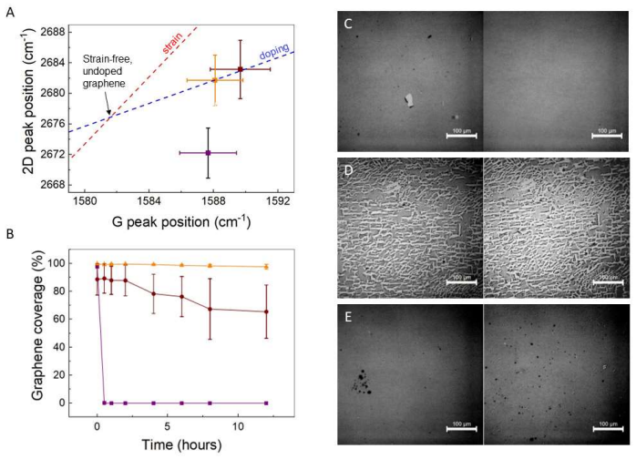
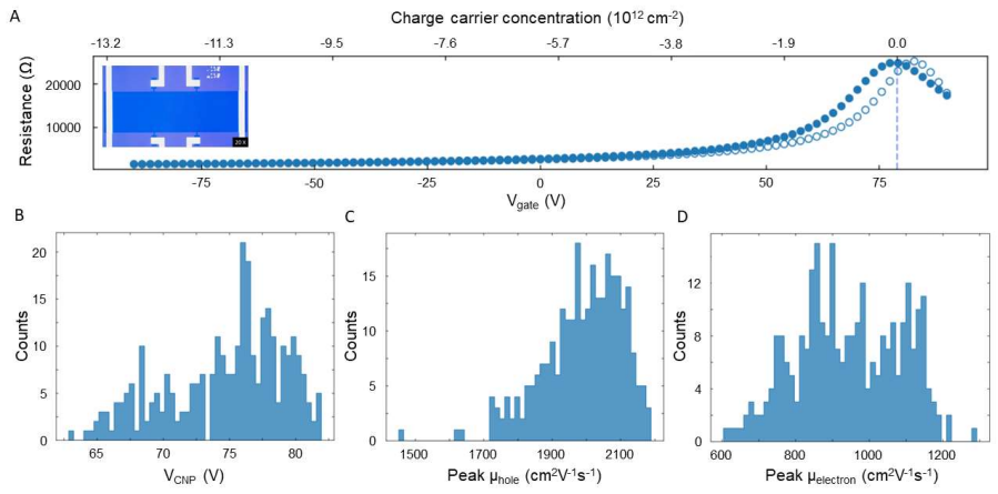
On the paper's own terms, the central discovery is that a pyrene-based molecular adhesion layer prevents water from undermining graphene on silicon wafers without degrading the electronic quality of the graphene. The layer is formed by first attaching aminopropyl groups to the oxide surface and then coupling 1-pyrenebutyric acid to them, leaving pyrene moieties that stack against graphene through π-π interactions. Under immersion in 0.5 M KOH, graphene coverage after 12 hours is 98% on pyrene-coated wafers versus 1% on bare wafers; in glacial acetic acid the numbers are 99% versus 30%, and in NMP 99% versus 3%. Devices built on pyrene-coated 4-inch wafers reached measurement yields of 86–99.7% (versus 31–89% on bare wafers, depending on oxide thickness) and showed similar hole and electron mobilities to devices on bare wafers. In sonication tests, all pyrene devices survived 20 minutes without an increase in resistance, while most devices on bare wafers failed; the pyrene devices also stayed essentially hysteresis-free, which the authors attribute to suppressed water intercalation.
Load-bearing premise
The wafer-scale yield claim assumes the bare and pyrene-coated wafers are otherwise equivalent, but the authors note the measured wafers were not necessarily from the same batch and that gate-capacitance profiles vary between batches, so part of the 99.7% versus 89.0% yield gap could come from wafer-batch differences rather than the pyrene layer.
Editorial extensions
If this is right
- Graphene field-effect transistors could be put through standard semiconductor cleaning and etching steps, including alkaline photoresist removers and NMP-based processes, without losing the graphene layer.
- Device fabrication on functionalized wafers can be scaled to full 4-inch wafers with near-100% measurement yield while keeping mobilities and charge-neutrality voltages comparable to devices on bare wafers.
- Liquid-gated graphene sensors could be regenerated or functionalized in harsh solvents and sonication baths, which are currently avoided for fear of delamination.
- The pyrene layer suppresses strain and doping in transferred graphene on the wafer scale, giving a more uniform starting material for device arrays.
Reading between the lines
- An implication the authors do not develop is that the pyrene layer could serve as a general platform for 2D materials beyond graphene, since any material with π-conjugated or van der Waals character may anchor through the same pyrene units.
- Because the wafer-scale yield comparison used BARE and PYRENE wafers that were not necessarily from the same batch, a direct same-batch comparison is the natural next test; the delamination results do not depend on this assumption, but the headline yield advantage does.
- The 3-day room-temperature coupling step is slow by industrial standards; a faster or plasma-assisted coupling variant would test whether the yield and robustness gains survive a production-compatible cycle time.
- Long-term stability beyond 12-hour immersions or repeated processing cycles is not reported; extrapolating the claimed robustness to device lifetimes of years assumes the pyrene-graphene interaction does not degrade with repeated wet/dry cycling.
Editorial analysis
A structured set of objections, weighed in public.
Referee Report
Summary. The paper reports a two-step covalent functionalization of Si/SiO2 wafers with a pyrene-based monolayer (via APTES silanization and HATU-mediated coupling of 1-pyrenebutyric acid). The authors characterize the modified surface (contact angle, AFM, XPS) and show that graphene transferred onto these wafers retains 98–99% coverage after 12 h in 0.5 M KOH, glacial acetic acid, or NMP, compared with 1–30% on bare wafers. Liquid-gated GFETs on pyrene-coated wafers survive sonication in acetone better than devices on bare or OTS/HMDS/PHEN-coated wafers. On full 4-inch wafers, the authors report a device measurement yield of 86.2% (285 nm oxide) and 99.7% (90 nm oxide) for pyrene-coated wafers, compared with 31.4% and 89.0% for bare wafers, with similar electronic properties.
Significance. If the coverage and delamination results hold, this is a practically relevant method for integrating CVD graphene into wafer-scale semiconductor processing, as it addresses a known water-intercalation delamination problem. The coverage data are direct, quantitative, and reproducible across three different harsh liquid environments, and the paper provides a plausible chemical mechanism (π–π interaction between pyrene and graphene). The work also includes a full-wafer demonstration with an industry partner, which strengthens the real-world relevance. However, the wafer-scale yield claim is less secure than the delamination data because of the measurement-yield definition and unmatched wafer batches.
major comments (2)
- [Results and discussion, Wafer-scale GFETs (Table 4)] The yield comparison is based on a metric that counts intact devices with VCNP outside the gate sweep as failures, and the BARE and PYRENE wafers are explicitly stated to be from unmatched batches. Therefore the yield gap (99.7% vs 89.0% on 90 nm oxide; 86.2% vs 31.4% on 285 nm oxide) cannot be directly attributed to the pyrene layer or to improved mechanical stability; a batch-dependent shift in doping or oxide capacitance would produce the same signature. The authors should either present a matched-wafer comparison, report a functional yield that is insensitive to VCNP location, or clearly restrict the claim to what the metric can support.
- [Results and discussion, Delamination tests (Table 3)] The delamination tests show that graphene coverage on pyrene-coated wafers remains high after immersion in KOH, acetic acid, and NMP, but no electrical measurements of these exposed films are presented. The title and abstract claim 'robust graphene electronics under industrial processing conditions,' yet the evidence for electronics robustness comes only from sonication experiments, not from the chemical-exposure tests. The authors should either include post-exposure transport measurements or rephrase the claims to distinguish adhesion/coverage robustness from electronic-device robustness.
minor comments (6)
- [General] The numbering of supplementary figures and tables is inconsistent: the main text cites Figure S1, S2, S3, S4 and Table S1, S2, but the supplementary section begins at Figure S5 and Table S5. This makes it difficult to locate the corresponding data and should be corrected.
- [Figure 3C-E] The optical micrographs of the delamination tests lack scale bars; please add them.
- [Table 2] The caption says 'dI/dVt=20min values are reported relative to ΔdI/dVt=0min' but the meaning of ΔdI/dV is unclear; please specify the normalization.
- [Wafer-scale GFETs] The gate sweep range used to define the measurement yield is not stated; please report it so the yield values are interpretable.
- [Table 4] The column labeled 'hyst' is not defined; if it is VCNP,forward - VCNP,backward, please say so.
- [Sonication experiments] With only four devices per surface, the sonication survival statistics (e.g., 4/4 for PYRENE vs 1/4 for BARE) have wide confidence intervals; please report individual data points or confidence intervals in Figure 2 and Table 2.
Circularity Check
No significant circularity: the paper's claims are supported by direct experimental measurements, with at most comparability caveats that are not circular reasoning.
full rationale
The paper is an experimental demonstration, not a derivation, and no predictive claim reduces by construction to its inputs. The functionalization is verified by contact angle, XPS, and AFM; graphene quality by Raman spectroscopy; adhesion/robustness by direct optical coverage measurements in KOH, acetic acid, and NMP; and electronic performance by transport measurements. The central delamination result (98% vs 1% coverage in KOH after 12 h) is a direct observation, independent of any fitted parameter or assumed mechanism. The wafer-scale device measurement yield is honestly defined as the fraction of devices with VCNP inside the sweep range, and the authors explicitly state that intact devices with out-of-range VCNP are excluded and that BARE and PYRENE wafers were not necessarily from the same batch. This is a limitation on the strength of the yield comparison, not circularity: the yield metric is not defined in terms of the pyrene layer, and the conclusion is not forced by the definition. Citations to prior work on pyrene-graphene interactions (refs 20-21) provide external context but are not load-bearing because the present paper's coverage and transport data stand on their own. No self-citation chain, imported uniqueness theorem, fitted input renamed as prediction, or ansatz smuggled via citation was found. The one caveat worth noting for correctness review is the unmatched-wafer comparison underlying the 99.7% versus 89.0% yield gap, but that is a statistical comparability issue, not a circularity issue.
Assumptions & free parameters
assumptions (5)
- domain assumption XPS C1s peak at 284.7 eV is attributed to sp2 carbon from pyrene moieties, confirming the covalent surface functionalization.
- domain assumption Graphene adhesion is mediated by pi-pi stacking between graphene and pyrene, and this is the cause of the observed delamination resistance.
- standard math Raman G versus 2D peak positions can be linearly decomposed into strain and doping components using the calibration of Lee et al. (ref 22).
- domain assumption Liquid-gating and back-gating mobility extraction assumes a standard capacitive model with known gate capacitance.
- domain assumption Optical inspection of a 150 micrometer central circle is a valid measure of graphene coverage and delamination.
Cite this review
Pith. "Pith review of Wafer-scale robust graphene electronics under industrial processing conditions." pith.science (2026). https://pith.science/paper/XV2WDFEB
@misc{pith2026250112963,
  author       = {Pith},
  title        = {Pith review of: Wafer-scale robust graphene electronics under industrial processing conditions},
  year         = {2026},
  howpublished = {\url{https://pith.science/paper/XV2WDFEB}},
  note         = {Machine review of arXiv:2501.12963}
}
read the original abstract
For commercial grade electronic devices, stable structures are required to ensure a long device life span. When such devices contain nanomaterials like graphene, it is crucial that these materials resist industrial processes and harsh environments. For environments that contain water, graphene delamination is a notorious drawback, as water intercalation and eventually liftoff readily occur in aqueous and especially in alkaline solutions. This limitation renders graphene incompatible with key wafer-processing steps in the semiconductor industry. In this work, a covalent pyrene-based adhesion layer is synthesized in a facile, two-step procedure. Through {\pi}-{\pi} interactions, the adhesion of graphene to silicon wafers was maintained under conditions that resemble harsh processes, i.e. acidic and alkaline solutions, several organic solvents, and sonication. Moreover, they could be produced with a device measurement yield up to 99.7% and reproducible device-to-device electronic performance on 4-inch silicon wafers. Our results show that a straightforward functionalization of silicon wafers with an adhesive layer can be directly applicable in industrial-scale fabrication processes, giving access to robust graphene field effect devices that are built to last long.
Figures


Figures from the paper (1 more)
Reference graph
Works this paper leans on
-
[1]
Electric field effect in atomically thin carbon films
Novoselov KS, et al. Electric field effect in atomically thin carbon films. Science 306, 666 (20/04)
-
[2]
The electronic properties of graphene
Castro Neto AH, Guinea F, Peres NMR, Novoselov KS, Geim AK. The electronic properties of graphene. Reviews of Modern Physics 81, 109-162 (2009)
work page 2009
-
[3]
Graphene photonics and optoelectronics
Bonaccorso F, Sun Z, Hasan T, Ferrari AC. Graphene photonics and optoelectronics. Nature Photonics 4, 611-622 (2010)
work page 2010
-
[4]
Mechanical and electromechanical properties of graphene and their potential application in MEMS
Khan ZH, Kermany AR, Öchsner A, Iacopi F. Mechanical and electromechanical properties of graphene and their potential application in MEMS. Journal of Physics D: Applied Physics 50, 053003 (2017)
work page 2017
-
[5]
Graphene and carbon nanotube (CNT) in MEMS/NEMS applications
Zang X, Zhou Q, Chang J, Liu Y, Lin L. Graphene and carbon nanotube (CNT) in MEMS/NEMS applications. Microelectronic Engineering 132, 192-206 (2015)
work page 2015
-
[6]
Graphene based sensors and biosensors
Justino CIL, Gomes AR, Freitas AC, Duarte AC, Rocha-Santos TAP. Graphene based sensors and biosensors. TrAC Trends in Analytical Chemistry 91, 53-66 (2017)
work page 2017
-
[7]
Graphene-based sensors for human health monitoring
Huang H , et al. Graphene-based sensors for human health monitoring. Frontiers in Chemistry 7, (2019)
work page 2019
-
[8]
Sensing at the Surface of Graphene Field-Effect Transistors
Fu W, Jiang L, van Geest EP, Lima LMC, Schneider GF. Sensing at the Surface of Graphene Field-Effect Transistors. Advanced Materials 29, 1603610 (2017)
work page 2017
Show all 31 references
-
[9]
Enhancement of the adhesion energy between monolayer graphene and SiO2 by thermal annealing
Megra YT, Lim S, Lim T, Na SR, Suk JW. Enhancement of the adhesion energy between monolayer graphene and SiO2 by thermal annealing. Applied Surface Science 570, 151243 (2021). 12
2021
-
[10]
Interfacial bonding characteristics between graphene and dielectric substrates
Das S, Lahiri D, Agarwal A, Choi W. Interfacial bonding characteristics between graphene and dielectric substrates. Nanotechnology 25, 045707 (2014)
2014
-
[11]
Graphene annealing: How clean can it be? Nano Letters 12, 414-419 (2012)
Lin Y-C, Lu C-C, Yeh C-H, Jin C, Suenaga K, Chiu P-W. Graphene annealing: How clean can it be? Nano Letters 12, 414-419 (2012)
2012
-
[12]
Clean graphene surface through high temperature annealing
Xie W, Weng L-T, Ng KM, Chan CK, Chan C-M. Clean graphene surface through high temperature annealing. Carbon 94, 740-748 (2015)
2015
-
[13]
Roll-to-roll green transfer of CVD graphene onto plastic for a transparent and flexible triboelectric nanogenerator
Chandrashekar BN, et al. Roll-to-roll green transfer of CVD graphene onto plastic for a transparent and flexible triboelectric nanogenerator. Advanced Materials 27, 5210- 5216 (2015)
2015
-
[14]
Fabrication of patterned silane based self- assembled monolayers by photolithography and surface reactions on silicon-oxide substrates
Herzer N, Hoeppener S, Schubert US. Fabrication of patterned silane based self- assembled monolayers by photolithography and surface reactions on silicon-oxide substrates. Chemical Communications 46, 5634-5652 (2010)
2010
-
[15]
Organized monolayers by adsorption
Sagiv J. Organized monolayers by adsorption. 1. Formation and structure of oleophobic mixed monolayers on solid surfaces. Journal of the American Chemical Society 102, 92-98 (1980)
1980
-
[16]
Surface chemical reactions on self-assembled silane based monolayers
Wang L, Schubert US, Hoeppener S. Surface chemical reactions on self-assembled silane based monolayers. Chemical Society Reviews 50, 6507-6540 (2021)
2021
-
[17]
Enhancing structural properties and performance of graphene-based devices using self-assembled HMDS monolayers
Ramadan S, et al. Enhancing structural properties and performance of graphene-based devices using self-assembled HMDS monolayers. ACS Omega 6, 4767-4775 (2021)
2021
-
[18]
Graphene on a hydrophobic substrate: Doping reduction and hysteresis suppression under ambient conditions
Lafkioti M, et al. Graphene on a hydrophobic substrate: Doping reduction and hysteresis suppression under ambient conditions. Nano Letters 10, 1149-1153 (2010)
2010
-
[19]
Relationship between the dipole moment of self-assembled monolayers incorporated in graphene transistors and device electrical stabilities
Ku GM, Lee E, Kang B, Lee JH, Cho K, Lee WH. Relationship between the dipole moment of self-assembled monolayers incorporated in graphene transistors and device electrical stabilities. RSC Advances 7, 27100-27104 (2017)
2017
-
[20]
Direct measurements of the interaction between pyrene and graphite in aqueous media by single molecule force spectroscopy: Understanding the π−π Interactions
Zhang Y, Liu C, Shi W, Wang Z, Dai L, Zhang X. Direct measurements of the interaction between pyrene and graphite in aqueous media by single molecule force spectroscopy: Understanding the π−π Interactions. Langmuir 23, 7911-7915 (2007)
2007
-
[21]
Measuring and manipulating the adhesion of graphene
Miskin MZ, Sun C, Cohen I, Dichtel WR, McEuen PL. Measuring and manipulating the adhesion of graphene. Nano Letters 18, 449-454 (2018)
2018
-
[22]
Optical separation of mechanical strain from charge doping in graphene
Lee JE, Ahn G, Shim J, Lee YS, Ryu S. Optical separation of mechanical strain from charge doping in graphene. Nature Communications 3, 1024 (2012)
2012
-
[23]
Raman spectrum of graphene and graphene layers
Ferrari AC, et al. Raman spectrum of graphene and graphene layers. Physical Review Letters 97, 187401 (2006)
2006
-
[24]
Understanding and controlling the substrate effect on graphene electron-transfer chemistry via reactivity imprint lithography
Wang QH, et al. Understanding and controlling the substrate effect on graphene electron-transfer chemistry via reactivity imprint lithography. Nature Chemistry 4, 724- 732 (2012)
2012
-
[25]
Controlled modulation of electronic properties of graphene by self-assembled monolayers on SiO2 substrates
Yan Z, Sun Z, Lu W, Yao J, Zhu Y, Tour JM. Controlled modulation of electronic properties of graphene by self-assembled monolayers on SiO2 substrates. ACS Nano 5, 1535-1540 (2011)
2011
-
[26]
Carrier control of graphene driven by the proximity effect of functionalized self-assembled monolayers
Yokota K, Takai K, Enoki T. Carrier control of graphene driven by the proximity effect of functionalized self-assembled monolayers. Nano Letters 11, 3669-3675 (2011)
2011
-
[27]
Large-scale graphene transistors with enhanced performance and reliability based on interface engineering by phenylsilane self- assembled monolayers
Liu Z, Bol AA, Haensch W. Large-scale graphene transistors with enhanced performance and reliability based on interface engineering by phenylsilane self- assembled monolayers. Nano Letters 11, 523-528 (2011)
2011
-
[28]
Work-function engineering of graphene electrodes by self-assembled monolayers for high-performance organic field-effect transistors
Park J , et al. Work-function engineering of graphene electrodes by self-assembled monolayers for high-performance organic field-effect transistors. The Journal of Physical Chemistry Letters 2, 841-845 (2011)
2011
-
[29]
Hysteresis of electronic transport in graphene transistors
Wang H, Wu Y, Cong C, Shang J, Yu T. Hysteresis of electronic transport in graphene transistors. ACS Nano 4, 7221-7228 (2010). 13
2010
-
[30]
Hysteresis modeling in graphene field effect transistors
Winters M, Sveinbjörnsson EÖ, Rorsman N. Hysteresis modeling in graphene field effect transistors. Journal of Applied Physics 117, 074501 (2015)
2015
-
[31]
Mechanism and suppression of physisorbed-water-caused hysteresis in graphene FET sensors
Bartošík M, et al. Mechanism and suppression of physisorbed-water-caused hysteresis in graphene FET sensors. ACS Sensors 5, 2940-2949 (2020). Supplementary Information Materials and methods Chemicals were purchased at Sigma Aldrich or Brunschwig Chemie and used without further...
2020
Reviewed August 10, 2026 · model on record in the stance chip above.
Discussion (0). Continue with ORCID to comment.