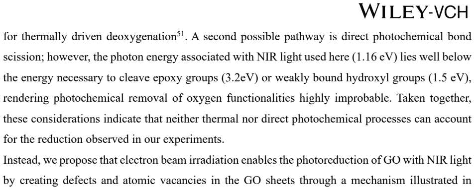
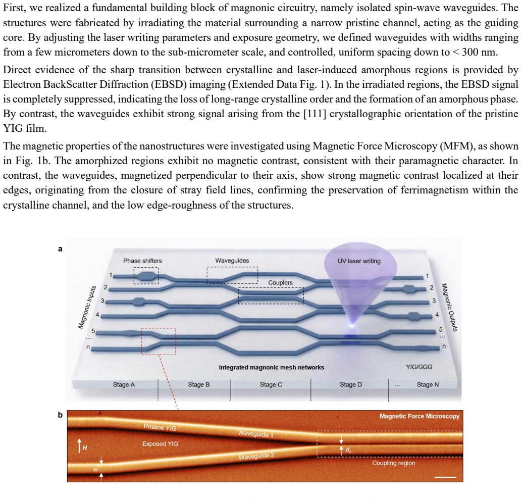
pith. machine review for the scientific record. sign in

physics.app-ph

Applied Physics

Applications of physics to new technology, including electronic devices, optics, photonics, microwaves, spintronics, advanced materials, metamaterials, nanotechnology, and energy sciences.

0
physics.app-ph 2026-05-14 2 theorems

Ultrasound identifiability set by forward structure and variability

Identifiability Limits in Ultrasonic Microstructure Characterisation: A Canonical and Stochastic Framework

Forward-map geometry and variance-weighted analysis show combined observables help but intrinsic spread still limits recovery of correlation

Figure from the paper full image
abstract click to expand
Ultrasound for microstructure characterisation is increasingly studied and is often assessed through inversion performance. However, the framework is fundamentally constrained by the information content available in the measured response. Hence, this work examines identifiability directly by analysing the geometry of the forward operator in both a canonical pulse-echo model and a stochastic surrogate microstructure. For the canonical model, a closed-form sensitivity analysis reveals information limits arising from parameter coupling, dimensional restriction, and interface-driven saturation. For the surrogate microstructures represented by Gaussian random fields, the forward map from correlation length $D$ and texture-coherence parameter $T$ to the attenuation and velocity observables remains structurally full rank. However, the sensitivity geometry is strongly anisotropic, with uneven parameter influence across the observable space. When intrinsic microstructural variability is incorporated, practical identifiability is further reduced. A variance-weighted Fisher framework shows that recoverability is governed by the balance between sensitivity magnitude and stochastic variability, rather than by structural rank alone. Inversion results confirm this behaviour: single observables produce elongated and weakly constrained objective landscapes, whereas combined observables improve conditioning through complementary sensitivities. These results show that, within the feature-level framework considered here, identifiability limits are governed primarily by forward-map structure and intrinsic variability, with direct implications for observable selection and measurement design.
0
0
physics.app-ph 2026-05-13 1 theorem

AC Harman underestimates module efficiency by 30 percent

Quantitative comparison of heat flow, guarded-heater and AC Harman methods for thermoelectric module efficiency

Heat flow and guarded heater methods match closely while boundary effects and radiation reduce the effective temperature difference in theAC

Figure from the paper full image
abstract click to expand
The evaluation of thermoelectric conversion efficiency remains challenging owing to the lack of internationally standardized measurement protocols. Commonly used techniques -- including the heat flow, guarded heater, and AC Harman methods -- differ fundamentally in their operating principles and sensitivity to heat losses. In this study, we benchmark three module-level efficiency measurement techniques -- the heat-flow, guarded heater, and AC Harman methods -- using commercial Bi$_2$Te$_3$-based modules with different substrates materials. The conversion efficiencies obtained using the heat flow and guarded heater methods showed good agreement within experimental uncertainty for temperature differences up to 70 K. In contrast, the AC Harman method underestimated the conversion efficiency by approximately 30 %. Through systematic measurements on modules with different substrates and detailed finite element simulations, this underestimation was attributed to boundary-condition effects and radiative heat dissipation, which significantly reduce the effective temperature difference developed across the module in the Harman configuration. These results highlight the limitations of the AC Harman method for quantitative conversion-efficiency evaluation under non-ideal thermal environments and emphasize the necessity of accounting for radiative and substrate-related heat losses. Nevertheless, with appropriate modeling and correction, strategies, the AC Harman method remains a viable tool for rapid performance screening. Our results provide a quantitative benchmark of major measurement techniques and contribute to clarify best practices for module-level thermoelectric metrology and guide method selection, fully supporting future efforts toward methodological standardization.
0
0
physics.app-ph 2026-05-12 Recognition

U-core windings cancel fluxes to enable ZVS Cuk converter

An Integrated Magnetics Design for an Isolated ZVS Cuk Converter

Placement sets coupling so DC flux vanishes and AC flux leaves just enough ripple for all switches to achieve zero-voltage switching, shown

abstract click to expand
This paper proposes a new integrated magnetics (IM) design for an isolated zero-voltage-switching (ZVS) Cuk converter (IZCC). In this design, six magnets are wound onto a single magnetic core, and to minimize magnetic core size and losses, both direct current (DC) and alternating current (AC) flux cancellations are considered. The DC flux is fully cancelled, and the AC flux must be cancelled until a limited value such that the input and output inductor currents have enough ripple to provide the conditions for achieving ZVS on all switches. Therefore, the value of the coupling coefficients (CC) between the windings should be considered such that the minimum ripple to achieve ZVS for all the switches is available. The design is implemented on a simple magnetic U-core, and the CC values are specified based on the winding locations and arrangement. To validate the idea experimentally, a hardware prototype is proposed with a power of 0.5 kW, a switching frequency of 150 kHz, and a peak efficiency of 97.25%.
0
0
physics.app-ph 2026-05-12 2 theorems

Imaginary-time evolution filters spectra and caps stable real-time reconstruction

Analytic Continuation Between Real- and Imaginary-Time Quantum Dynamics and the Fundamental Instability of Inverse Reconstruction

Low-energy features remain recoverable inside a defined bandwidth while higher frequencies are lost irreversibly due to scale-dependent map

Figure from the paper full image
abstract click to expand
We develop a unified spectral-semigroup framework that connects real-time and imaginary-time quantum dynamics through analytic continuation. Within this formulation, evolution is expressed as an exponential reweighting of spectral components generated by a single operator $\mathcal{G}$, placing unitary and dissipative dynamics on equal footing within a common spectral structure. The mapping naturally induces a nonlocal fractional operator in time, giving rise to a contractive semigroup governed by a square-root spectral deformation and identifying imaginary-time evolution as an effective fractional low-pass filter. While exponential attenuation suppresses high-frequency components, the inverse transformation remains systematically controllable within a well-defined spectral window. In this regime, stable reconstruction of low-energy and coarse-grained dynamical features is achieved, establishing a predictive relation between imaginary-time evolution and recoverable information. This leads to a quantitative description of a bandwidth-resolved asymmetry between forward propagation and inverse recovery. Across systems with continuous and discrete spectra, few-level coherence, and non-Hermitian generators, we demonstrate that spectral structure governs reconstruction fidelity in a unified manner. In particular, non-Hermitian and open-system settings reveal that irreversibility emerges as a geometry- and scale-dependent feature of the spectrum, tied to both damping and eigenstate non-orthogonality. These results recast analytic continuation as a structured, scale-dependent filtering process with quantifiable and systematically accessible reconstruction limits, providing a unified perspective on the interplay between dynamics, spectral geometry, and information recovery.
0
0
physics.app-ph 2026-05-12 1 theorem

CNIS design delivers 1% energy resolution for cold neutrons

Physical design of cold neutron direct geometry inelastic spectrometer at China Spallation Neutron Source

Bent guides and flexible choppers at CSNS enable high-resolution studies of low-energy excitations starting in 2029.

Figure from the paper full image
abstract click to expand
The Cold-Neutron Inelastic Spectrometer (CNIS) is a direct-geometry, time-of-flight instrument designed for China Spallation Neutron Source (CSNS) and optimized to probe low-energy lattice and magnetic excitations. The instrument integrates a long flight path with bent supermirror guides and an elliptical-focusing geometry to suppress high-energy background while improving cold-neutron delivery to the sample. A flexible multi-disk chopper suite provides pulse shaping, band selection and monochromatization, enabling multi-$E_\textrm{i}$ operation. Modular features, including an interchangeable high-focusing guide insert, radial collimation and a vacuum ``airbox'' for simplified sample-environment integration, enhance signal-to-noise and operational versatility. Through combined flight-path and chopper optimization, CNIS achieves excellent routine-mode energy resolution and can reach approximately $\sim 1\%$ in a dedicated high-resolution configuration. CNIS is planned to commence user operation in 2029, offering a highly flexible platform for cold-neutron inelastic scattering studies.
0
0
physics.app-ph 2026-05-11 Recognition

Heap shape analysis yields unique DEM parameters for powders

From Angle of Repose to Heap Morphology: Full-Field Calibration of DEM for Granular Powders

Pixel-wise comparison of full experimental and simulated heap profiles overcomes non-uniqueness in angle-of-repose calibration for cohesive

Figure from the paper full image
abstract click to expand
The calibration of discrete element method (DEM) models is commonly performed by tuning model parameters to match an experimental measurements, most commonly the angle of repose (AOR). Although widely used, AOR-based calibration metrics do not adequately characterize the full heap morphology, particularly when dealing with cohesive granular materials. As a result, AOR-based calibrations often leads to non-unique parameter sets. In this work, we propose a DEM calibration procedure based on full-field image analysis of static powder heaps rather than scalar AOR measurements. The method compares an average experimental heap profile (AEHP), obtained from repeated GranuHeap experiments, with an average numerical heap profile (ANHP) generated from DEM simulations. This comparison is performed using pixel-wise grayscale intensity values of both average heap profiles. Two metal powders commonly used in additive manufacturing, Ti6Al4V and Al6061, are used to evaluate the proposed methodology. This work highlights the limitations of traditional AOR-based approaches and demonstrates that full-field heap morphology offers a more reliable framework for DEM calibration.
0
0
physics.app-ph 2026-05-11 Recognition

Time modulation dynamically tunes resonances in metasurfaces

Time-Controlled Resonances in 2-D Metasurfaces via Equivalent Circuits

Equivalent circuits from Floquet expansions show how temporal control enables multi-band responses in thin structures.

Figure from the paper full image
abstract click to expand
This work introduces a semi-analytical frequency-domain framework for the analysis of two-dimensional, time-modulated (2+1)-D metasurfaces controlled by PIN diodes. The formulation focuses on the unit-cell level, modeled as a waveguide discontinuity problem, where the space-time periodicity of the structure enables the representation of scattered fields via Floquet expansions. After appropriate mathematical treatment, these expansions lead to an equivalent circuit description of the metasurface, providing physical insight into its spatiotemporal scattering behavior and facilitating the design of reconfigurable electromagnetic devices. The model is employed to explore key phenomena present in space-time systems, such as frequency mixing and spatiotemporal scattering. In addition, dynamic tuning is explored in resonant metasurfaces, where time becomes an additional degree of freedom for the design. The dynamic control of resonances opens a new way to explore multi-band and wideband behaviors from very thin metasurfaces under temporal coupling.
0
0
physics.app-ph 2026-05-11 2 theorems

Reciprocal-space model gives spin-wave dispersion for dipolar bilayers

Reciprocal Space Approach to Dipolarly Coupled Magnetic Hetero-Structures

Analytic access to symmetric and antisymmetric modes in exchange-decoupled magnetic layers separated by a spacer.

Figure from the paper full image
abstract click to expand
We present an analytical framework capable of describing spin-waves dynamic in magnetic hetero-structures composed of a pair of exchange-decoupled magnetic layers separated by a nonmagnetic spacer, focusing in particular on garnet-based multilayers. The model captures the formation of collective spin-wave modes, namely symmetric and antisymmetric, arising from dipolar coupling and provides direct access to the dispersion relation of the system and consequent interference phenomena. This formalism establishes a versatile theoretical tool for the predictive design of dipolarly coupled magnonic devices, providing access to their eigenfrequencies and mode shapes.
0
0
physics.app-ph 2026-05-08

AC current triggers reverse heat flow for local cooling

Reverse heat flow with Peltier-induced thermoinductive effect

Exact solution shows the thermoinductive effect occurs universally in solids and strengthens with thermoelectric properties, verified by 25m

Figure from the paper full image
abstract click to expand
The concept of "thermal inductance" expands the options of thermal circuit design. However, the inductive component is the only missing components in thermal circuits, unlike their electromagnetic counterparts. Herein, we report an electrically controllable reverse heat flow, in which heat flows from a low-temperature side to a high-temperature side locally and temporarily in a single material by imposing thermal inertia and an ac current. This effect can be regarded as an equivalent of the "thermoinductive" effect induced by the Peltier effect. We derive an exact solution indicating that this reverse heat flow occurs universally in solid-state systems and that it is considerably enhanced by thermoelectric properties. A local cooling of 25 mK is demonstrated in (Bi,Sb)2Te3, which is explained by our exact solution. This effect can be directly applied to the potential fabrication of a "thermoinductor" in thermal circuits.
0
0
physics.app-ph 2026-05-06

Sparse regression identifies initial gaps in piecewise-linear systems

Data-driven Initial Gap Identification of Piecewise-linear Systems using Sparse Regression and Universal Approximation Theorem

Approximating governing equations as sums of piecewise-linear functions lets the switching gap be calculated from coefficients and points.

Figure from the paper full image
abstract click to expand
This paper proposes a method for identifying an initial gap in piecewise-linear systems from data. Piecewise-linear systems appear in many engineered systems such as degraded mechanical systems and infrastructures, and are known to show strong nonlinearities. To analyze the behavior of such piecewise-linear systems, it is necessary to identify the initial gap, at which the system behavior switches. The proposed method identifies the initial gap by discovering the governing equations using sparse regression and calculating the gap based on the universal approximation theorem. A key step to achieve this is to approximate a piecewise-linear function by a finite sum of piecewise-linear functions in sparse regression. The equivalent gap is then calculated from the coefficients of the multiple piecewise-linear functions and their respective switching points in the obtained equation. The proposed method is first applied to a numerical model to confirm its applicability to piecewise-linear systems. Experimental validation of the proposed method has then been conducted with a simple mass-spring-hopping system, where the method successfully identifies the initial gap in the system with high accuracy.
0
0
physics.app-ph 2026-05-06

Diffractors leave mode spacing unchanged in reverberation chambers

Effect of Adding Wave Diffractors Within Reverberation Chambers on the Frequency Spacing of Adjacent Resonant Modes

Differences in adjacent resonant frequencies fall within measurement uncertainties.

Figure from the paper full image
abstract click to expand
This paper takes advantage of a recent method able to extract the characteristics of resonant modes in a metallic enclosure such as a reverberation chamber (RC). The aim here is to analyze, the effect of inserting curvilinear objects within a parallelepiped RC on the chamber performances, particularly from the point of view of the frequency spacing of adjacent resonant modes. Two configurations are compared: one is a parallelepiped RC with added curvilinear diffracting objects, and the other is the same chamber without diffractors but with added absorbers to compensate the decrease of the quality factor. The obtained results exhibit differences that fall within the measurement uncertainties.
0
0
physics.app-ph 2026-05-06

Double coils triple wireless power output under misalignment

Analysis and Design of Double-Transmitting Coil Systems based on Parity-Time Symmetry

A PT symmetry system with parallel transmitters and a custom negative resistance circuit keeps voltage steady within 3.4 percent.

abstract click to expand
The wireless power transfer (WPT) system based on parity-time (PT) symmetry has the advantages of robustness, stability, and efficient power transmission. However, traditional PT symmetry structures have limited voltage power output and are susceptible to horizontal misalignment effects. Multiple transmission coils have been proven to improve the power and misalignment tolerance of WPT systems, but variations in inter-coil coupling significantly affect transmission power. Towards this end, this article proposes a double-transmitting coil WPT system based on PT symmetry, which is innovative in that a novel negative resistance structure based on operational amplifier (OA) is proposed, and the parallel structure of double-transmitting coil is applied to this negative resistance structure. Compared with the traditional WPT system based on a single-transmitting coil PT, this system improves the power and misalignment tolerance in the PT symmetry region. The large-sized and small-sized receiving coils increase the load power to 313% and 185% respectively. Moreover, in the symmetry region, the displacement of the receiving coil in the horizontal and vertical directions results in variations of the equivalent coupling coefficient, which can achieve stable power transmission in three dimensions. The voltage fluctuation rate of both receiving coils does not exceed 3.4%, greatly improving the degree of freedom of the receiving system.
0
0
physics.app-ph 2026-05-06

Errors found in EC2 chronoamperometry paper

Critical study of A. Eswari and S. Sarvana kumar, "Chronoamperometric response of electrochemical reaction diffusion system: a new theoretical and numerical investigation for EC2 scheme", in J. Iran. Chem. Soc. 21(8), (2024), 2183-2199

A critical study identifies incorrect mathematics and results by comparing against independent simulations of the reaction-diffusion system.

Figure from the paper full image
abstract click to expand
The title paper is discussed critically. There are major problems with incorrect statements, irrelevant citations, incorrect mathematics leading to incorrect results, which are compared with our own simulations.
0
0
physics.app-ph 2026-05-06

WGAN maps EM targets to switchable dual-band FSS topologies

WGAN based Inverse Design of Active Dual Band FSS with Switchable Transmission

The model generates pin-diode structures that keep high-frequency transmission while switching low-frequency behavior, with over 90 percent,

abstract click to expand
This letter presents a novel design method for switchable dual band transmissive frequency selective surface (FSS). The proposed FSS possesses characteristics of maintaining passband characteristics at high frequencies, while switching from transmission to reflection at low frequencies with pin diodes states altering. Specifically, we propose a crystal growth-based topology generation strategy, and utilize a simplified U-Net Wasserstein GAN (WGAN) neural network model to establish an inverse mapping model from electromagnetic response to structure topology parameters. The trained WGAN achieves training and validation accuracies of 95.59% and 90.84%, while the simplified U-Net attains training and validation accuracies of 98.5% and 94.1%. Using the trained WGAN. The generated structural topologies were validated through full-wave simulations and experimental measurements. The proposed method enhances the design flexibility and overcomes the time- consuming drawbacks of conventional FSS design.
0
0
physics.app-ph 2026-05-06

Acoustic waves modulate second-harmonic light at 226 MHz

Ultrafast acoustic modulation of second-harmonic generation in monolayer transition metal dichalcogenides

Synchronized measurements link surface strain directly to nonlinear optical response in atomically thin layers, enabling high-speed control.

Figure from the paper full image
abstract click to expand
High-speed modulation and deterministic control of optical nonlinear processes in nanomaterials are essential for realizing future nanoscale optoelectronic devices. Applying strain is a ubiquitous and versatile approach to deform atomically thin materials, allowing direct modification of their electronic and optical properties. Yet, strain engineering of nonlinear processes has so far relied predominantly on static approaches, which inherently limit modulation speed, reproducibility, and device scalability. Here, we demonstrate ultrafast acoustic modulation of second-harmonic (SH) generation in monolayer transition metal dichalcogenides using surface acoustic waves (SAWs). By employing a fully phase-synchronized SH measurement combined with stroboscopic surface displacement detection, we directly visualize dynamic SH modulation at a frequency of 226 MHz. Moreover, theoretical modeling and determination of photoelastic coefficients enable quantitative extraction of the SAW-induced dynamic strain. Our results establish a direct link between acoustic fields and optical nonlinearities, providing a robust platform for dynamic strain engineering in two-dimensional nanophotonic devices.
0
0
physics.app-ph 2026-05-05

Fredholm mapping turns thermal blur into virtual waves

Generalized Virtual-Wave Theory for Photothermal Coherence Tomography under Arbitrary Excitation Toward Non-Contact Industrial Inspection of Composite Materials

Arbitrary heating waveforms are converted to propagating fields that sharpen defect depth in composites

Figure from the paper full image
abstract click to expand
Photothermal imaging is a powerful noncontact and nondestructive technique for subsurface inspection of composite materials, yet its performance is fundamentally limited by the diffusive and irreversible nature of heat transport, leading to severe image blurring and ambiguous depth interpretation. The concept of virtual waves provides a route to overcome this limitation by linking diffusion fields to propagating wave fields, but existing approaches are largely restricted to idealized impulsive excitation. Here, we propose a generalized virtual-wave photothermal tomography framework that extends the diffusion-to-wave transformation to arbitrary boundary excitations, including pulsed, harmonic, and chirped waveforms. Starting from the heat equation with a general source term, we derive a Fredholm integral mapping between the measured diffusion field and a virtual wave field governed by a wave equation, explicitly enforcing causality and thermodynamic irreversibility. The resulting ill-posed inverse problem is solved using ADMM or truncated SVD, depending on the excitation characteristics. Numerical and experimental results demonstrate that the proposed method converts blurred thermal responses into wave-like fields with clear wavefronts and reflections, enabling improved depth localization and tomographic reconstruction. Experiments on carbon fiber reinforced polymer samples with embedded defects show enhanced contrast, sharper boundaries, and more reliable depth interpretation compared with conventional thermographic techniques. This work establishes a unified and physically grounded framework for wave-based photothermal tomography under realistic excitation conditions.
1 0
0
physics.app-ph 2026-05-04 2 theorems

Nanogaps in NbTi resonators raise cryogenic sensitivity by 10x

Surface nanostructuring of NbTi superconducting thin-film resonators for enhanced cryogenic thermometry

Lowering critical temperature 1.5 K produces 62 MHz/K response at 4.2 K for better ultra-cold monitoring.

Figure from the paper full image
abstract click to expand
The rising complexity of cutting-edge cryogenic systems is currently imposing challenging technical constraints to the monitoring of ultra-cold temperatures through standard commercially available sensors. Among different alternative technologies, superconducting microwave resonators have been recently investigated as ideal candidates for performing on-chip cryogenic thermometry, in reason of their intrinsically low power dissipation, typically large temperature sensitivities and excellent sub-mK resolution below 10 K. In such a framework, through this study we aim at demonstrating the possibility to enhance the temperature performance of superconducting microwave resonators by means of surface nanostructuring. More specifically, different arrays of nanogaps are strategically patterned on the inductive line of a 1.3 GHz planar resonator, by partially etching a Nb50Ti50 thin film, in order to tune the critical transition of the material and, therefore, increase the curvature of the fres(T) response. Although the presence of such weak-links introduces larger microwave losses, a 1.5 K decrease of TC is recorded, which directly translates into an enhancement of the temperature sensitivity by a factor 10, with respect to a reference non-nanostructured sensor. In particular, a maximum value of dfres/dT = 62 MHz/K, at 4.2 K, is achieved for the device showing the largest nanogap width of about 350 nm, demonstrating that the surface nanostructuring of superconducting thin-films can be effectively engineered to enhance the temperature response of microwave resonators for high-performance cryogenic thermometry. We believe that similar approaches might be investigated and, eventually, adopted for the near-future development of the next generation of low-temperature sensors.
0
0
physics.app-ph 2026-05-04

Live imaging cuts antiviral testing time by 26 hours

Continuous quantification of viral plaque dynamics using ultra-large-area label-free imaging enables rapid antiviral susceptibility testing

Continuous label-free tracking shows how drug doses delay and block plaque growth, yielding results days earlier than stained endpoint tests

Figure from the paper full image
abstract click to expand
The plaque reduction assay (PRA) remains the gold standard for antiviral susceptibility testing, evaluating drug potency by measuring reductions in plaque-forming units (PFUs). However, the traditional PRA is time-consuming, labor-intensive, prone to manual counting errors, and offers limited scalability. Moreover, its reliance on destructive fixation and chemical staining reduces the assay to a static, endpoint observation, obscuring the dynamic, time-resolved kinetics of dose-dependent viral inhibition. Here, we introduce a label-free, time-resolved PRA platform that transforms the conventional assay into a continuous, high-dimensional measurement of viral infection dynamics. Our system integrates a compact lens-free imaging setup with a custom-designed ultra-large-area (100 cm^2) thin-film transistor (TFT) image sensor and deep learning-based algorithms to autonomously quantify PFU dynamics within an incubator. Validated using herpes simplex virus type-1 (HSV-1) treated with acyclovir, the platform matched chemically-stained ground truth measurements with zero false positives while accelerating readout by ~26 hours. Crucially, our system revealed that increasing drug concentrations induce temporally distinct delays and suppress new PFU formation, enabling conclusive drug efficacy evaluations within ~60 hours post-infection. This scalable, label-free framework redefines antiviral susceptibility testing as a rapid, time-resolved and information-rich measurement framework, providing a generalizable platform for virology research, high-throughput drug screening, and clinical diagnostics.
0
0
physics.app-ph 2026-05-04

MOSFET circuit keeps IRS phase shift at 180 degrees past 1 W

Numerical Validation of a MOSFET-Based Control Circuit for High-Power Intelligent Reflecting Surfaces for Wireless Power Transfer Applications

Back-to-back switches plus capacitors suppress nonlinearity so binary reflection control survives high-power wireless transfer conditions.

Figure from the paper full image
abstract click to expand
Intelligent reflecting surfaces (IRSs) have attracted considerable attention because of their ability to dynamically control electromagnetic wave propagation. While most existing IRSs have been developed for low-power communication and sensing applications, their extension to high-power wireless power transfer (WPT) environments remains largely unexplored, as the high induced currents can damage or saturate the sensitive control elements, disrupting their tuning functionality. Here, we propose a metal-oxide-semiconductor field-effect transistor-based (MOSFET-based) binary control circuit for IRSs operating at 2.4 GHz that can withstand input power levels exceeding 1 W per unit cell. The control circuit employs a back-to-back MOSFET switching topology with series and parallel capacitors to suppress impedance variations arising from device nonlinearity while maintaining a reflection phase difference of approximately 180 degrees between the ON and OFF states. A theoretical model based on transmission lines is developed and validated against full-wave co-simulations incorporating nonlinear SPICE device models. The dynamic range is evaluated with respect to both the rated current and the reflection phase difference, demonstrating stable operation up to 1.25 W. Supercell-level beam steering is further demonstrated through far-field simulations, confirming active control of the reflection angle via switching pattern reconfiguration. These results establish a foundation for the deployment of IRSs in high-power WPT scenarios.
0
0
physics.app-ph 2026-05-04

Skin sensor reconstructs 3D shapes to 0.62 mm accuracy in 0.1 s

A skin-like conformal sensor for real-time shape mapping

A 5-by-5 strain-gauge array maps continuous deformations without cameras, even under combined stretch, bend, and press.

Figure from the paper full image
abstract click to expand
Reliable real-time 3D shape sensing is essential for robust control and interpretation of deformable systems during motion. Existing vision-based approaches require line-of-sight and complex instrumentation, limiting operation in occluded and space-constrained settings. Here, we introduce a scalable, skin-like sensor that reconstructs its continuous 3D deformation in real time from distributed strain measurements. The device embeds a 2D array of mirror-stacked, printed oxidized eutectic gallium-indium (o-EGaIn) strain gauges within an elastomeric film to measure off-neutral-axis strains. Combined with a mechanics-informed observation model and a fast optimization routine, the system estimates local curvature, elongation, offset, and orientation under concurrent stretching, bending, and indentation, enabling reconstruction of complex surfaces. A 5-by-5 array with a 12 mm pitch achieves a mean surface reconstruction error of 0.62 mm with 0.1s latency across all tested scenarios. When conforming to complex surfaces, the sensor provides fast 3D shape mapping of the underlying geometry. Demonstrations involving palm gesturing, finger indentation, and contact-induced balloon deformation highlight utility for epidermal motion tracking, haptic interaction, and intraoperative monitoring.
0
0
physics.app-ph 2026-05-04

Electron beam pre-treatment lets one laser pulse reduce graphene oxide in 960 ns

Fast reduction of electron-beam-activated graphene oxide by an infrared laser pulse

Defects raise near-infrared absorption and drive oxygen diffusion, cutting reduction time for thin films to under a microsecond.

Figure from the paper full image
abstract click to expand
Rapid and controllable reduction of graphene oxide (GO) remains a critical challenge for realizing its full technological potential. Here, we report efficient reduction of GO by a synergistic electron-beam-assisted single-pulse near-infrared (NIR) laser process. Time-resolved electron energy-loss spectroscopy measured with a dynamic transmission electron microscope (DTEM) is used to locally track the oxygen concentration evolution after NIR laser pulse irradiation. This finds an oxygen diffusivity of 1.6 +/- 0.4 x 10$^{-8}$ m$^2$/s, which corresponds to 90% reduction of a 46-nm thick film within 960 ns. Electron beam irradiation is found to change the optical absorptivity of GO in the NIR region and the thermal heating cycle resulting from the laser pulse is simulated. Structural characterization via selected-area electron diffraction (SAED) and high-resolution transmission electron microscopy (HRTEM) finds localized restoration of sp$^2$ bonding accompanied by turbostatic disorder in the reduced GO. Together, these results point to a mechanism involving the creation of defects and vacancies produced by electron beam irradiation, which increases the efficiency of NIR light absorption and oxygen diffusion normal to the layers. This study demonstrates the important role of such defects in controlling the photochemistry of GO and its response to NIR illumination.
0
0
physics.app-ph 2026-05-04

NV centers on anvil diamond track iron's magnetic loss to 30 GPa

High-pressure magnetic transition in iron observed via diamond quantum sensing

Quantum imaging shows the stray field drop that marks the alpha-to-epsilon transition inside a pressure cell.

Figure from the paper full image
abstract click to expand
Diamond quantum sensors offer high precision and spatial resolution as magnetic probes, making them promising for a wide range of applications. While diamond anvil cells (DACs) can generate extremely high pressures, techniques for magnetometry under such conditions remain limited. By fabricating an ensemble of NV centers directly on the anvil diamond surface, we enable precise magnetic measurements under high pressure. In this work, we employ this NV ensemble to image the stray magnetic field of iron up to 30 GPa, enabling the observation of the magnetic transition ($\alpha$-$\varepsilon$ transition) in iron.
0
0
physics.app-ph 2026-05-04

Multiplication shares excess energy with hot carriers in TMD cells

Fundamental Efficiency Limits of Transition-Metal Dichalcogenide Solar Cells with Carrier Multiplication and Hot-Carrier Effects

A detailed-balance model shows carrier multiplication cannot exceed the reversible hot-carrier limit and adds almost no gain for high-gap 2D

Figure from the paper full image
abstract click to expand
Detailed-balance limits for transition-metal dichalcogenide (TMD) solar cells have been reported, but existing TMD-specific limits do not simultaneously resolve thickness-dependent optics, carrier multiplication (CM), hot-carrier (HC) extraction, and finite cooling leakage. Here, we develop a generalized detailed-balance theory that provides an upper-bound framework. The model combines energy- and thickness-dependent absorptance a(E,d), exciton-resolved monolayer absorbance, an experimentally available CM quantum-yield limit (eta_CM <= 0.97), and an endoreversible HC engine with ideal energy-selective contacts and finite heat-leak coefficient kappa. The framework shows that CM and HC draw on the same above-gap photon-energy reservoir; therefore, CM does not raise the reversible HC thermodynamic limit. Instead, CM can protect finite-kappa performance only by shifting excess-energy utilization from a cooling-sensitive voltage channel into collected current. For optically thick TMDs under AM1.5G illumination, the SQ optimum lies near E_g = 1.3 eV, whereas the CM/HC-favored envelope shifts toward E_g = 1.0 eV with reversible efficiencies above 50%. For monolayer TMDs such as WSe2 (E_g = 1.63 eV), CM is essentially inactive because only about 3.7% of above-gap AM1.5G photons satisfy E > 2E_g, giving an idealized short-circuit-current gain of only about 0.6% before device nonidealities. Bulk-like TMDs can show large HC-related gains at d = 10-50 nm, but even kappa = 0.2 W m^-2 K^-1 implies about 100 W m^-2 heat leak for Delta T = 500 K. Thus, high-E_g monolayer TMDs are not promising one-sun CM candidates, whereas narrow-E_g, bulk-like TMD absorbers remain plausible beyond-SQ candidates only if energy-selective extraction and phonon-engineered cooling suppression are realized together.
0
0
physics.app-ph 2026-05-01

Laser writing builds programmable magnonic meshes for chip RF routing

Programmable Integrated Magnonic Meshes

Seven-stage networks with six inputs and outputs keep spin-wave coherence without amplification, scaling magnonic circuitry.

Figure from the paper full image
abstract click to expand
Integrated circuits are a cornerstone of modern information technology, and analog wave-based architectures could enable fast and efficient processing beyond conventional charge electronics. In magnonics, spin waves provide a highly tunable, compact and energy-efficient medium for on-chip microwave signal transport and processing. However, progress has been limited to isolated elements or short devices, severely limiting the overall functional complexity and scalability. Here we realize the key elements of universal magnonic circuitry, using a single-step direct laser writing process in yttrium iron garnet, and monolithically cascade them in multi-stage programmable devices and networks. Using magneto-optical Kerr effect microscopy, we show efficient spin-wave propagation and preserved phase coherence in waveguide structures for hundreds of wavelengths. In coupled waveguides, we observe complete and periodic power transfer over several coupling lengths, and in phase shifters we achieve arbitrary, tunable phase delays. By cascading these elements, we realize programmable splitters, frequency demultiplexers, and phase-controlled 2x2 routers, where output power and relative phase can be programmed on demand via external fields. Finally, we realize programmable magnonic interferometric meshes for on-chip radio-frequency signal routing, with up to six magnonic inputs and outputs and seven cascaded stages, without the need for intermediate amplification. These direct-write cascaded networks bridge a long-standing gap in magnonic scalability, offering a viable pathway toward integrated, large-scale architectures for both classical and quantum processing.
0
0
physics.app-ph 2026-05-01

Alumina coating stabilizes NV centers in diamond nanopillars at 6 K

Stabilisation of NV centres in diamond nanopillars at low temperature

Coated pillars keep single-photon purity and brightness steady under laser light in vacuum, while uncoated ones degrade, enabling use in non

Figure from the paper full image
abstract click to expand
Degradation of near surface nitrogen vacancy (NV) centers in diamond under optical illumination has restricted their deployment in applications such as scanning NV magnetomety, particularly under harsh environment such as low temperatures and vacuum. Previously, alumina passivation of planar diamond samples has been shown to reduce the degradation of near surface ensemble NV centers in vacuum. Here, we expand this study to incorporate photonic nanostructures by analyzing the single photon emission characteristics of NV centers embedded in an array of alumina-coated diamond nanopillars in high vacuum and low temperature (6K, high vacuum) environments under non-resonant (522 nm) laser exposure. We find that, in contrast to the oxygen-terminated diamond nanopillars, NV centers in the alumina-coated nanopillars demonstrate negligible change in the single photon purity and brightness over the course of laser exposure in vacuum. At low temperature, NV centers under alumina termination demonstrate stable single photon emission, whereas under oxygen termination the single photon purity degrades under high intensity laser exposure. Alumina surface passivation is therefore shown as a viable path toward the realization of robust NV-diamond based nanoscale sensing under non-ambient atmospheric environments, including using diamond scanning probes.
1 0
0
physics.app-ph 2026-05-01

Ovonic switches let hardware neurons add and divide

Neuronal arithmetic operators based on Ovonic threshold switches (OTS) for biologically inspired analog computing

Circuits achieve biological-style summation and divisive gain control, delivering order-of-magnitude gains in energy and scale over CMOS.

abstract click to expand
Biological neurons perform arithmetic computations - including additive integration and divisive gain modulation - through synaptic conductance changes and shunting inhibition, enabling context-dependent information processing that far exceeds simple threshold-and-fire models. Replicating these capabilities in compact hardware remains a fundamental challenge for neuromorphic engineering. Here, we demonstrate artificial neuron circuits based on Ovonic threshold switches (OTS) that physically implement three arithmetic operations: SUM, PARALLEL, and DIVISION. The SUM and PARALLEL neurons exploit MOSFET-controlled dendritic conductances, producing output firing rates that collapse onto invariant curves as a function of combined inputs - satisfying the canonical criteria for neuronal addition. The DIVISION neuron leverages a JFET-based shunting pathway, inspired by GABA_A-mediated inhibition in the cortex, to achieve divisive gain modulation well described by a Hill-type function (R2 ~ 0.95, Hill exponent n ~ 1.3), consistent with nonlinear normalization observed in visual and olfactory circuits. Applying the DIVISION neuron to pixel-wise image normalization under non-uniform illumination recovers obscured visual content, mirroring contrast normalization in the visual cortex. Compared to CMOS-based division implementations, the proposed approach offers improvements in energy efficiency and scalability exceeding an order of magnitude, establishing a viable path toward compact, brain-inspired analog computing.
0
0
physics.app-ph 2026-04-30

NiOx Ga2O3 diodes reach over 10 kV breakdown with 2.3 GW/cm2 PFOM

VBr >10 kV E-Beam/Sputtered Vertical NiOx/(011) β-Ga2O3 HJDs with PFOM >2.3 GW/cm2

The edge-terminated vertical devices extract a record 5.3 MV/cm field in thick (011) drift layers.

Figure from the paper full image
abstract click to expand
Beta-gallium oxide (\beta-Ga2O3) holds enormous potential for medium voltage range power electronic applications. This work reports VBr > 10 kV/Ron,sp = 43 m\Omega*cm2 class edge terminated vertical heterojunction diodes (HJDs) with e-beam/sputtered nickel oxide (NiOx) stack on epitaxial (011) \beta-Ga2O3. The power figure of merit (PFOM) of the HJD exceeds 2.3 GW/cm2. The extracted parallel plane breakdown field is > 5.3 MV/cm, which is the highest reported electric field for thick (011) \beta-Ga2O3 epitaxial drift layer.
0
0
physics.app-ph 2026-04-30

Interface cuts let finite metamaterials beat classical dampers

Unveiling the key role of Interfaces in the Design of finite-sized Metamaterial Structures

Varying the unit-cell boundary in sandwich panels changes vibration performance enough to outperform standard civil-engineering solutions.

Figure from the paper full image
abstract click to expand
This paper investigates the influence of interfaces on the performance of finite-sized mechanical metamaterial structures for vibration damping applications. The metamaterial structures are designed in a sandwich configuration in which two homogeneous plates are connected to a metamaterial array. We test four different arrays that are obtained from the same metamaterial by differently cutting the metamaterial's unit cell at the metamaterial/plate interface. When the four unit cells are periodically repeated in space, they create the same infinitely large metamaterial with an identical mechanical response. In finite-sized structures, however, the different interfaces between the metamaterial array and the plates~--~called ``material interfaces''~--~and between the metamaterial and the air~--~called ``free interfaces''~--~strongly affect the specimen's vibration transmission characteristics. Using experimental measurements and validated finite-element (FE) models, we demonstrate a significant influence of the different types of interfaces on the global responses and local displacement fields of the structures. We also demonstrate the presence of a vibroacoustic coupling in the structures which also depends on the type of metamaterial/plate interfaces. Furthermore, we explore optimization strategies for enhancing the vibration damping performance of the metamaterial structures considering not only the metamaterial array but also the adjacent structures (the homogeneous plates). A comparison with benchmark cases illustrates the optimization potential that the interfaces' design offers for the vibration damping capability of finite-sized metamaterial structures. We show that optimizing the type of targeted interfaces can shift a metamaterial's response from underperforming to significantly outperforming compared to classical solutions for noise and vibration damping in civil engineering.
0
0
physics.app-ph 2026-04-30

Frequency separates two light-strain effects in semiconductors

Dynamic disentanglement of photoflexoelectricity and flexophotovoltage

Oscillating cantilever tests on perovskites distinguish photoflexoelectricity from flexophotovoltage via unique frequency and phase patterns

abstract click to expand
The coupling between light and strain gradients shows two kinds of effects: light enhanced flexoelectricity (photoflexoelectricity) and gradient enhanced photovoltage (flexophotovoltage). Although these effects originate from fundamentally different physical mechanisms (one is light enhanced electromechanical coupling, the other is a bulk photovoltaic effect), in this article we show that dynamic flexoelectric measurements of semiconductors under illumination intrinsically contain contributions from both. To allow disentangling them, we have developed a general theoretical framework for their combined response in oscillating systems, demonstrating that the two contributions can be unambiguously separated through their distinct frequency and phase dependencies. We have validated these predictions using oscillating cantilever measurements on centrosymmetric perovskite semiconductors (SrTiO3 and methylammonium lead bromide, MAPbBr3), obtaining selfconsistent values for the coefficients both effects which are in excellent agreement with independent static measurements. Our results establish a general protocol for disentangling both light strain gradient couplings using only oscillatory measurements, and clarify the interpretation of flexoelectric measurements under illumination.
0
0
physics.app-ph 2026-04-30

The paper introduces a multi-fidelity Bayesian optimization method to inversely design…

Inverse Design of Cellular Composites for Targeted Nonlinear Mechanical Response via Multi-Fidelity Bayesian Optimisation

Multi-fidelity Bayesian optimization enables efficient inverse design of spinodoid cellular composites to achieve targeted nonlinear…

abstract click to expand
The rise of machine learning and additive manufacturing has enabled the design of architected materials with tailored properties that surpass those of natural materials. Inverse design offers a data-efficient alternative to trial-and-error methods, yet most existing approaches depend on either large datasets or scarce high-fidelity data from simulations and experiments. These requirements pose a particular challenge for architected materials with nonlinear mechanical responses, where capturing complex deformation modes requires expensive evaluations. To address this, a Multi-Fidelity Bayesian Optimisation (MFBO) framework for the inverse design of cellular composites that directly targets their full nonlinear response is introduced. By integrating information from multiple fidelity sources and scalarising the response using a similarity score, the framework enables efficient exploration of the design space while reducing reliance on costly evaluations. As a proof of concept, the method is applied to spinodoid cellular composites using finite element models, validated with compression tests on short carbon-fibre reinforced PET-G composites. Four target responses were considered, with three multi-fidelity strategies benchmarked against a standard single-fidelity approach. Across all cases, MFBO achieved higher similarity scores and consistently recovered the targeted responses, outperforming the single-fidelity baseline under the same evaluation budget, while also successfully recovering all targeted responses. These results demonstrate the effectiveness of MFBO for inverse design of stochastic architected materials, where high-quality data is scarce but lower-cost proxies exist. By efficiently navigating complex design spaces, MFBO enables the creation of cellular composites with precisely tailored nonlinear mechanical behaviour.
0
0
physics.app-ph 2026-04-29

Quantum random walk reproduces all crystal diffraction effects

A unified quantum random walk model for internal crystal effects in dynamical diffraction

One framework now handles temperature gradients, Talbot fringes, and angled faces inside dynamical diffraction intensity patterns.

Figure from the paper full image
abstract click to expand
The theory of dynamical diffraction (DD) in perfect crystals is the backbone of high-precision neutron and X-ray diffraction experiments, enabling accurate determination of crystal structure factors and the realization of perfect crystal interferometers. In practice, however, real crystals exhibit deformations and imperfections, including surface roughness, defects, temperature gradients, angled crystal faces, and curvature, that degrade interferometer performance and are difficult to model using conventional DD theory, particularly in complex geometries. To address these challenges, a quantum information (QI) model for DD has been under development, with demonstrated experimental agreement for both ideal crystals and in the presence of some imperfections such as surface roughness and defects. Here, we present a unified quantum random walk model that is now suitable for reproducing all established DD effects. We demonstrate this by incorporating a broad range of internal crystal effects influencing DD intensity distributions, including linear temperature gradients, the DD Talbot effect, and angled or miscut crystals. These results establish the QI model as a comprehensive and flexible framework for experimental analysis, as well as for the design of next-generation perfect crystal neutron interferometers and neutron optical components, such as condensing monochromators.
0
0
physics.app-ph 2026-04-29

NV centers achieve nanoscale deuterium NMR at low fields

Quantum sensing-enabled deuterium NMR spectroscopy with nanoscale sensitivity at low magnetic fields

Statistical spin fluctuations provide six-to-eight-order sensitivity boost while operating at fields two orders of magnitude weaker than in

Figure from the paper full image
abstract click to expand
Nuclear magnetic resonance (NMR) spectroscopy provides unparalleled access to molecular structure and dynamics but is traditionally limited by weak signal strength, requiring large sample volumes and high magnetic fields. Here, we demonstrate nanoscale deuterium (2H) NMR spectroscopy using nitrogen vacancy (NV) centers in diamond, reproducing the characteristic quadrupolar powder line shapes that are present in the conventional bulk NMR spectra. By detecting statistical spin fluctuations from nanometer scale detection volumes, our approach delivers a sensitivity enhancement of six to eight orders of magnitude over inductive detection while operating at magnetic fields two orders of magnitude lower than those used in conventional NMR. Temperature dependent measurements of a deuterated polymer and molecular solid reveal distinct motional averaging and phase transitions with nanoscale sensitivity. Powder-like NV detected 2H NMR establishes a powerful tool for probing molecular dynamics on the nanoscale and, in the ultimate limit, at the single molecule level - capabilities beyond those of most existing spectroscopic techniques.
0
0
physics.app-ph 2026-04-29 Recognition

MEMS clock reaches 8 parts-per-trillion stability over 8 hours

A micromechanical frequency reference with parts-per-trillion holdover stability

Dual-frequency resonance tracking removes electronic gain drift, matching chip-scale atomic clocks in a compact silicon device.

Figure from the paper full image
abstract click to expand
Microelectromechanical (MEMS) resonators are widely used in timekeeping applications, and recent advances in fabrication, materials, and encapsulation technology have advanced their potential as high stability frequency references. However, for holdover applications that require the highest levels of long-term frequency stability, compact vapor atomic clocks remain dominant. In this work, we demonstrate a 268 MHz MEMS clock that achieves record fractional frequency stability of ~8 parts-per-trillion at an averaging time of 8 hours, competitive with chip-scale atomic clocks. We achieved this using a single-crystal silicon electrostatic resonator that has no currently known intrinsic drift mechanism and is protected from the environment with a wafer-level encapsulation. We specifically identify gain variations in the sustaining electronics as the dominant limitation in conventional phase-locked oscillator architectures -- originating from temperature sensitivity and drifts in the electronic components -- and overcome this by implementing a frequency-locked loop architecture based on dual-frequency resonance tracking (DFRT). This novel approach removes the specific gain of the supporting electronics as a frequency determining variable in the oscillator. When combined with dual-mode tracking and ratiometric temperature stabilization of the resonator, this approach enables a dramatic enhancement to long-term frequency stability and establishes gain-insensitive DFRT locking as a general paradigm for high-stability MEMS clocks.
0
0
physics.app-ph 2026-04-28

Metasurface yields reflector-free high-Q acoustic waves in liquids

Reflector-Free, Highly Confined Love-Like SAWs Enabled by a Phononic Metasurface for Real-Time Monitoring of Cell Dynamics

Zero radiation losses and strong confinement enable real-time cell death monitoring without traditional reflectors.

Figure from the paper full image
abstract click to expand
Surface acoustic wave (SAW) devices are widely used in sensing and biosensing but generally suffer from strong attenuation in liquid environments. Conventional approaches rely on reflectors to reduce these losses, yet these components remain difficult to optimize: limited device miniaturization, and increase fabrication complexity. Here, we introduce an innovative design strategy that integrates a phononic metasurface with tailored electromechanical properties of the substrate to generate a type of shear-horizontal (SH) surface resonance modes that exhibit strong lateral confinement and zero radiation into both the substrate bulk and the free surface, eliminating the need for reflectors. This approach enables highly tailorable surface acoustic resonances with distinctive enhanced dynamic strain-energy confinement leading to significantly higher quality factors than conventional SAW devices, particularly in water-loaded conditions. We show the fabrication and experimental validation of the proposed phononic metasurface-based SAW resonator and showcase its biosensing capabilities through real-time monitoring of cellular death.
0
0
physics.app-ph 2026-04-28

Acoustic metasurface multiplexes holograms on velocity components

Vectorial Acoustic Multiplexed Holography

Physics-informed design separates vx, vy, and pressure channels with high fidelity and low crosstalk in experiments.

abstract click to expand
Encoding more information into wave fields is a central goal in imaging, communication, and wave control. Optical holography benefits from polarization multiplexing, but acoustic holography remains largely limited to pressure-only encoding because sound in fluids lacks naturally independent vector channels. Here, we show that particle velocity can serve as a practical multiplexing degree of freedom despite the intrinsic pressure-velocity coupling governed by the acoustic Euler equation. We develop a physics-informed inverse-design approach that incorporates acoustic propagation and pressure-velocity coupling to create a binary metasurface for vector-field acoustic holographic multiplexing. Experiments demonstrate dual-channel multiplexing on the in-plane velocity components v_x and v_y, and further extend to three-channel multiplexing by incorporating pressure p, with high-fidelity reconstruction and low cross-talk. This approach adds a new information dimension without reducing spatial or spectral bandwidth and enables broader forms of wave-based information encoding and multiplexed wave control.
0
0
physics.app-ph 2026-04-28

Double-layer LiTaO3 hits 25.7% coupling for SH2 mode

Complementary-polarity double-layer LiTaO3 resonators for symmetry-selective SH2 excitation with ultrahigh electromechanical coupling (kt² = 25.7%)

Opposite polarizations in bonded films match the vibration mode symmetry for efficient high-frequency acoustics

Figure from the paper full image
abstract click to expand
We report a structurally simple double-layer lithium tantalate (LiTaO3) bulk acoustic resonator that enables symmetry-selective excitation of the second-order thickness-shear (SH2) mode with ultrahigh electromechanical coupling. Two 31 deg Y-oriented single-crystal LiTaO3 films are rotation-bonded with complementary polarization (+X/-X) and driven by a longitudinal electric field. Matching between the effective piezoelectric symmetry and the SH2 mode yields an effective electromechanical coupling coefficient of kt^2 = 25.7% at 5.24 MHz. To our knowledge, this is the highest kt^2 reported for a LiTaO3 resonator architecture to date. The measured response is dominated by the target SH2 mode, with only weak parasitic features in the operating band. The structure is also tunable: the resonance frequency and coupling can be adjusted through geometric parameters while maintaining stable modal behavior, indicating good process tolerance. Finite-element analysis further suggests straightforward frequency scaling beyond 5 GHz by reducing the film and electrode thickness while preserving approximately 25% kt^2. In addition, introducing a SiO2 compensation layer is predicted to improve the temperature coefficient of frequency to approximately -25 ppm/deg C. These results establish complementary-polarity double-layer LiTaO3 as a practical platform for high-coupling, spurious-suppressed acoustic resonators and provide a scalable route toward wideband ultrasonic resonators, filters, and related transducers.
0
0
physics.app-ph 2026-04-28

Ion damage reaches 11.5 μm deep in β-Ga2O3 except on (001)

Evidence of Micron-Scale Ion Damage in (010), (110), and (011) {β}-Ga₂O₃ Epitaxial Layers

Sputtering and plasma etching reduce donor density by over 80 percent in three orientations while leaving the fourth largely intact.

abstract click to expand
We report on the experimental observation of up to 11.5 ${\mu}m$ deep charge depletion in (010), (110), and (011) ${\beta}-Ga_2O_3$ epitaxial layers due to ion damage from sputtering and inductively coupled plasma (ICP) etching processes whereas charge depletion in (001) ${\beta}-Ga_2O_3$ epitaxial layers was minimal. The orientation-dependent reduction in CV-measured charge density was first observed in $NiO_x$ reactively sputtered heterojunction p-n diodes (HJDs). When compared to reference low-damage Schottky barrier diodes (SBDs), the sputtered HJDs showed a $9.4{\times}$ increase in the specific on resistance $(R_{on,sp})$ and 85% reduction in net donor concentration $(N_D - N_A)$ at zero bias for sputter-damaged HJDs on (010) epitaxial layers whereas HJDs on (001) remained unchanged. Similarly, sputtered SiO2 caused a reduction of $N_D - N_A$ 11.5 ${\mu}m$ deep into the (010) material. Next, SBDs were fabricated on ${\beta}-Ga_2O_3$ surfaces previously etched via a BCl3 based ICP process and compared to SBDs on un-etched surfaces. The (010) SBDs on etched surfaces exhibited a $7.7{\times}$ increase in $R_{on,sp}$ and a 91% reduction in $N_D - N_A$ at zero bias where the (001) etched diodes exhibited little change. Additionally, (110) and (011) diodes fabricated on ICP damaged surfaces also saw a ~82% reduction in $N_D - N_A$ at zero bias, indicating (110) and (011) are also susceptible to ion damage. Damage in the (010), (110), and (011) diodes is potentially caused by energetic ions that travel into the open channels present along the [010] direction and create compensating point defects which could potentially diffuse further.
1 0
0
physics.app-ph 2026-04-28

Bias voltage turns soft membranes into pressure sensors

Pressure sensing by electro-mechanical coupling in compliant dielectric membranes polarized by a bias voltage

Capacitance shifts in nearly incompressible silicone rubber produce measurable voltage under deformation, unlike stiff piezoelectrics.

Figure from the paper full image
abstract click to expand
Among smart materials, piezoelectric materials occupy a very prominent position for sensing and actuation functions. Combined with simple or more advanced shunts, they are also proposed in various vibration mitigation schemes. However, the selection of available piezoelectric materials is mainly limited to ceramics (with an elastic modulus in the order of 10 Gpa (e.g. PZT ceramics) and a few polymer materials, with elastic modulus in the range of 1 Gpa (e.g. PVDF). In both cases, the high mechanical impedance and, consequently, the small dynamic strains limit the application of these materials to stiff structures. In this contribution, we discuss using a bias voltage to polarize dielectric materials and thereby compensate for the lack of spontaneous polarization observed in piezoelectrics. This enables access to materials with a wider range of elastic properties, such as soft elastomers, e.g. poly(dimethylsiloxane). As an example, we present a practical implementation of a silicone rubber membrane used as a highly compliant dynamic pressure sensor. For such nearly-incompressible materials, the capacitance change during dynamic deformation of the membranes is sufficiently large to generate a measurable dynamic voltage change over the membrane.
0
0
physics.app-ph 2026-04-27

Tri-element co-doping stabilizes n-type diamond

The boron-hydrogen-phosphorus tri-elements co-doped stable N-type single crystalline Diamond

Electron density exceeds phosphorus concentration and matches boron and hydrogen levels, giving low resistivity and strong UV output.

abstract click to expand
Diamond is an outstanding semiconductor for extreme electronics, yet reproducible n-type doping remains a long-standing challenge. Here we demonstrate stable n-type single-crystal diamond grown in a single step by a precisely controlled boron-hydrogen-phosphorus co-doping strategy. Hall measurements yield electron concentrations up to 1.0*1019 cm-3 with a resistivity as low as 0.249 ohmic.cm. Secondary-ion mass spectrometry shows that tri-elements doping is the key for achieving n-type conductivity as the electron density exceeds the incorporated phosphorus concentration and is the same level of that of hydrogen and boron concentrations, supporting a donor mechanism beyond an isolated substitutional phosphorus or just boron-hydrogen co-doping. Temperature-dependent photoluminescence (PL) reveals this tri-elements codoping method induces the impurity band, and the donor level is quite shallow around 61.6 meV, consistent with the temperature dependent resistance measurements. Moreover, the co-doped diamond also exhibits strong ultraviolet emission near 270-285 nm, and the internal quantum efficiency is estimated to be 69.4%, while the undoped diamond or only boron doped diamond shows negligible UV emission. These results establish a practical route to low-resistance high luminous n-type diamond and its based chips.
0
0
physics.app-ph 2026-04-24

TiO2 plate disinfects well water in 10 minutes under sun

Solar photocatalytic disinfection of well water using immobilized TiO₂: A comparative field study with SODIS in Antananarivo

Field study shows complete coliform inactivation in all samples versus 51% reduction with standard SODIS, for low-cost rural use.

Figure from the paper full image
abstract click to expand
Access to safe drinking water remains a major challenge in rural areas of developing countries. This study investigates the feasibility of a simple, low-cost solar photocatalytic reactor coated with commercial titanium dioxide (TiO$_2$) for the disinfection of well water contaminated with fecal coliforms. A TiO$_2$ film was deposited on a glass plate using a straightforward acetone slurry method and exposed to natural sunlight in Antananarivo, Madagascar. The efficiency was compared to the conventional SODIS method (solar disinfection without catalyst). Water samples from ten different wells were characterized for physicochemical parameters and bacteriological quality. After only 10 minutes of solar exposure, the photocatalytic reactor achieved complete inactivation (0 CFU/100 mL) of fecal coliforms for all ten samples tested, whereas the SODIS control only reduced the initial count by approximately $51\%$ in a representative sample. While disinfection kinetics varied slightly with water turbidity and pH, complete inactivation was consistently achieved. The results demonstrate that even a non-uniform, low-purity TiO$_2$ coating significantly accelerates bacterial disinfection under solar radiation, offering a promising and affordable household-scale treatment technology for low-resource settings.
0
0
physics.app-ph 2026-04-24

Three-nTron gate detects SNSPD coincidences on chip

Reconfigurable Superconducting Logic for On-Chip Photon Coincidence Detection

Bias-programmable circuit performs AND/XOR/OR at 4.2 K with error rates below 3 percent and drives modulator loads.

Figure from the paper full image
abstract click to expand
Scaling photonic quantum-information platforms requires arrays of superconducting nanowire single-photon detectors (SNSPDs) for feedforward control, in which optical operations are conditioned on preceding Bell-state measurements that typically rely on photon coincidence detections. On-chip superconducting cryotron electronics, performing logic directly on detector outputs and subsequently driving optical modulators, could substantially reduce latency and room-temperature interconnect complexity for feedforward schemes. To date, no cryotron logic gates specifically designed to process SNSPD outputs for quantum applications have been demonstrated. We demonstrate a bias-programmable logic gate based on three nanocryotrons (nTrons), fabricated using the same thin-film technology as SNSPDs. The circuit implements selectable AND (coincidence), XOR (odd-parity), and OR functions on two externally generated electrical pulses at 4.2 K, with bit-error rates below $10^{-3}$, bias margins up to $\pm24\%$, and operation extending to 25 MHz over narrower bias windows. Moreover, it performs coincidence and odd-parity detection on two co-fabricated SNSPDs' outputs with bit-error rates below $3.2 \times 10^{-2}$. As a proof-of-concept, we show that nTrons can drive capacitive loads up to 1.15 V, potentially enabling compatibility with electro-optic modulators in feedforward schemes.
0
0
physics.app-ph 2026-04-24

Surrogate cuts thermoreflectance fitting from hours to minutes

A transfer-learning-enhanced POD-FNN surrogate for rapid signal prediction and inverse fitting in thermoreflectance with patterned transducers

POD-FNN network with transfer learning predicts each signal in 0.01 s instead of 5 s and completes inverse fits in 65 s rather than five-and

abstract click to expand
Patterned-transducer thermoreflectance enhances sensitivity to low-thermal-conductivity materials by suppressing lateral heat spreading in the metal transducer, but its wider use is limited by the cost of repeated high-fidelity forward evaluations in iterative fitting. Here, we develop a transfer-learning-enhanced POD-FNN surrogate for rapid phase prediction in patterned-transducer thermoreflectance, using patterned FDTR as a representative case. A validated COMSOL model is first constructed, and proper orthogonal decomposition is applied directly to the phase signals to build a compact reduced-order representation. A feedforward neural network is then trained to predict the POD coefficients from thermophysical and geometric parameters. Within the original parameter domain, the surrogate achieves mean and median RMSE values of 0.19 and 0.17 degrees, with a maximum RMSE below 0.47 degrees, while reducing the average prediction time per signal from 5.39 s to 0.01 s (about 534x). In inverse analysis, the fitting time for a representative case is reduced from about 18950 s to about 65 s with comparable accuracy. The framework is further applied to measured Al/SiO2 samples, yielding stable silica thermal conductivities of 1.44 +/- 0.088, 1.43 +/- 0.093, and 1.50 +/- 0.079 W/(m K) for conventional FDTR and patterned FDTR with pattern radii of 5.3 and 3.25 um, respectively. Transfer learning further improves performance in expanded parameter domains, with the TL-FR strategy giving the best overall results. Reducing the additional target-domain dataset from 6000 to 1000 samples also lowers the high-fidelity data-generation time from about 34179 s to about 5885 s. The proposed framework provides an accurate and efficient route for repeated forward evaluation, rapid inverse fitting, and cost-effective model updating in patterned thermoreflectance workflows.
0
0
physics.app-ph 2026-04-24

Skull-conforming lenses focus ultrasound through the cranium

Skull-Conforming Acoustic Holographic Lenses for Transcranial Targeting

Personalized holographic interfaces encode wavefront corrections and couple efficiently to deliver accurate deep-brain pressure fields.

Figure from the paper full image
abstract click to expand
Transcranial focused ultrasound (tFUS) offers noninvasive access to deep brain circuits but remains limited by skull-induced phase aberration, acoustic impedance mismatch, and poor volumetric control of intracranial pressure fields. Conventional phased-array and planar holographic strategies compensate aberrations electronically or computationally, yet do not resolve geometric and coupling inconsistencies imposed by subject-specific cranial morphology. We introduce personalized skull-conforming acoustic holograms that physically encode individualized wavefront corrections into a conformal acoustic interface. Within a subject-specific volumetric holography (SSVH) framework, cranial geometry and therapeutic constraints are embedded into a physics-based optimization pipeline for holographic phase synthesis. The resulting lens is integrated with a skull- and skin-conforming coupling layer that enhances impedance continuity, reduces reflection losses, and stabilizes spatial alignment, enabling simultaneous aberration mitigation and efficient transcranial transmission. Numerical simulations across multiple subjects and targets demonstrate consistent volumetric focusing and reliable target coverage while maintaining pressure fields within safety limits. Experimental validation using an ex vivo human skull confirms accurate fabrication, effective acoustic coupling, and faithful reconstruction of designed three-dimensional acoustic fields. By unifying wavefront engineering with anatomical conformity, this work establishes skull-conforming acoustic holography as a scalable strategy for high-fidelity, anatomically adaptive transcranial ultrasound targeting.
1 0
0
physics.app-ph 2026-04-23

Safe active learning tests Ga2O3 sensors with one unsafe trial

Autonomous Reliability Qualification of Ga₂O₃-based Hydrogen and Temperature Sensors via Safe Active Learning

Framework monitors rectification to expand stress conditions safely and forecast long-term degradation trends.

abstract click to expand
We present a Safe Active Learning (SAL) framework for autonomous reliability characterization of rectifying Ga$_2$O$_3$-based devices under coupled thermal and hydrogen stress. SAL treats rectification as a device-physics-motivated safety observable and models its evolution over elapsed time, temperature, and H$_2$ concentration using a Gaussian-process surrogate. To handle condition-dependent and uncertain experiment durations, the method combines an adaptive completion-time window, time-window lower-confidence-bound safety checks, a trust region anchored to previously verified safe conditions, and a two-phase strategy that transitions from conservative safe exploration to progressively relaxed rectification targets as the device degrades. We first evaluate SAL in simulation, where it safely expands the explored region while learning the evolving rectification surface. We then demonstrate SAL experimentally on an automated high-temperature probe-station platform using a Pt/Cr$_2$O$_3$:Mg/$\beta$-Ga$_2$O$_3$ device. In the reported campaign, phase 1 incurred only one unsafe measurement associated with spurious current-voltage sweeps, while phase 2 intentionally probed lower-rectification regimes. Finally, we use the curated SAL dataset for offline long-horizon forecasting of device response at a target voltage using a structured Gaussian-process model with a condition-dependent Kohlrausch--Williams--Watts mean and a residual covariance kernel. The model captures long-time, saturating degradation trends in an auxiliary validation dataset, illustrating how safety-aware autonomous experimentation enables both conservative characterization and subsequent degradation modeling. Although demonstrated here for a rectifying Ga$_2$O$_3$ device, SAL is applicable to other systems where a measurable in situ safety observable can be defined.
0
0
physics.app-ph 2026-04-23

Reflector coating lifts PV yield by 1-2.4 percent yearly

How do sub-bandgap reflectors affect the performance of PV modules?

Reflecting unused infrared light cools silicon modules, adding 1-2% yearly output and up to 4% over 30 years via slower degradation.

Figure from the paper full image
abstract click to expand
Sub-bandgap reflectors (SBR) can reduce the temperature of photovoltaic (PV) modules by reflecting the near-infrared region of the solar spectrum with photon energies smaller than the electronic bandgap of the solar cell absorber material. We consider an ideal SBR, which reflects 100 % of non-harvestable low-energy photons but does not alter the reflectivity of the PV module for usable high-energy photons, and estimate how reducing the module temperature with the SBR affects the annual and the cumulative energy yield of silicon PV modules for six locations in North America and Europe. An ideal SBR would increase the annual energy yield between 1.0 % and 1.5 % for open-rack mounted modules and between 1.6 % and 2.4 % for close-roof mounted PV modules. Whether a non-ideal SBR provides a benefit in actual deployments strongly depends on the location and the optical properties of the coating. Beyond effects on the instantaneous power conversion efficiency and hence the annual energy yield, reducing the temperature by a SBR might also reduce the degradation and increase the overall lifetime of the PV module. By describing degradation using a simple Arrhenius approach using typical activation energies between 0.4 eV and 0.8 eV, we find that an ideal SBR increases the cumulative energy yield over 30 years between 2.2 % and 4.0 % for an open-rack mounted PV module in Princeton, New Jersey, USA.
0
0
physics.app-ph 2026-04-23

Bilayer TFLN cuts residual stress gradient by up to 80 percent

Gradient Residual Stress in Transferred Thin-Film Lithium Niobate and Its Compenstation Using Periodically Poled Piezoelectric Bilayers

Cantilever tests show opposite crystal orientations in stacked films reduce bending and enable stable MEMS devices.

Figure from the paper full image
abstract click to expand
In this work, we experimentally investigate the gradient stress (sigma1) in 128 deg Y-cut transferred thin film lithium niobate (TFLN) films with thicknesses from 100 to 460 nm using cantilever curvature analysis. The results reveal a strong dependence of sigma1 on both crystallographic orientation and film thickness, with stress-free orientations at approximately 55 deg and 125 deg for 220-460 nm films, shifting to approximately 20 deg and 160 deg for 100 nm films. The extracted normalized sigma1 ranges from -0.1 to 3.4 MPa/nm (100 nm), -0.8 to 0.34 MPa/nm (220 nm), and -0.12 to 0.08 MPa/nm (460 nm), indicating a pronounced thickness-dependent through-thickness stress gradient. Finite element simulations show excellent agreement with the measurements, validating the curvature-based extraction method and confirming that sigma1 originates from an orientation-dependent residual stress gradient. To mitigate this effect, a bilayer TFLN structure with opposite crystallographic orientations, forming a periodically poled piezoelectric film (P3F), is investigated, enabling partial cancellation of sigma1. A 90/110 nm P3F bilayer reduces the equivalent normalized sigma1 to -0.4 to -0.04 MPa/nm, resulting in significantly reduced deformation. These results establish gradient stress engineering through orientation, thickness, and bilayer design as an effective strategy for achieving mechanically stable and scalable TFLN microelectromechanical systems (MEMS) devices.
0
0
physics.app-ph 2026-04-22

Vowel shapes alter radio-wave passage through the head

Articulatory movements influence electromagnetic wave transmission through the vocal tract

Simulations and measurements show that different mouth positions produce distinct transmission curves between 1 and 6 GHz.

Figure from the paper full image
abstract click to expand
This study experimentally validates a numerical model of electromagnetic propagation through the human head during the pronunciation of different vowels, with the goal of improving our understanding of the underlying physical phenomena. A realistic finite element model was created from magnetic resonance images acquired while pronouncing the vowels /a/, /i/, and /u/. The model was validated against scattering matrix measurements obtained from two subjects whose geometries were modeled. Despite several potential sources of discrepancy, the simulations and measurements showed good qualitative agreement, confirming the validity of the approach. Similar transmission coefficient patterns were observed across subjects for the same vowels. Within the investigated frequency range of (1-6 GHz), the electric field exhibited a Mie scattering pattern. Local minima and maxima in the transmission coefficient, characterizing different articulatory configurations, were correlated with local variations in the electric field amplitude. The transmission coefficient's shape results from an interplay between resonance patterns and antenna placement, while the degree of mouth opening influences the shape of scattering modes. Although technically challenging, this numerical approach proved effective for studying electromagnetic propagation in the human head. The resulting robust numerical model and improved understanding of the underlying physics are expected to facilitate the development of radio-frequency-based silent speech interfaces.
0
0
physics.app-ph 2026-04-22

Acoustic trap force ratio varies non-monotonically with pressure

Competition between acoustic radiation force and streaming-induced drag force in focused beams for 3D cell trapping

Streaming velocity scales with a lower power of pressure than radiation force once flow becomes inertial, so higher drive does not always,

Figure from the paper full image
abstract click to expand
The ability to trap a single cell or microparticle in three dimensions is important for biomedical and microfluidic applications. Single-beam acoustic tweezers based on focused waves provide a compact and biocompatible approach because of their high spatial resolution and strong intensity gradients. However, 3D trapping remains challenging, especially at high frequencies, because the weak axial restoring radiation force may not overcome the pushing drag force caused by acoustic bulk streaming in free space. The combined effect of acoustic radiation force and streaming-induced drag force on a microparticle has not been systematically studied. Although the radiation force scales with the square of the focal pressure amplitude p_foc, the scaling of streaming-induced drag force with p_foc under different flow conditions remains unclear. Here, we establish a unified theoretical and numerical framework to compare these two effects and derive an explicit scaling law, U0 ~ p_foc^n, for the streaming velocity from the viscous to the inertial regime. We show that n = 2 in the viscous limit (Re_lambda << 1), n = 4/3 in the inertial limit (Re_lambda >> 1), and n lies between 4/3 and 2 in the transition regime (Re_lambda ~ 1). We further introduce the Schiller-Naumann model to estimate the drag force more accurately than the Stokes model. On this basis, we find that the ratio of axial radiation force to drag can vary non-monotonically with p_foc, contrary to the conventional expectation of monotonic increase. This work provides a theoretical basis for optimizing single-beam acoustic tweezers for stable 3D trapping of single cells.
0
0
physics.app-ph 2026-04-21

Reverse bias creates 100x more mobile ions in perovskite diodes

Electrochemical reactions under reverse bias create additional mobile ions that enable hole tunneling in metal halide perovskite diodes

The extra iodine vacancies enable hole tunneling currents that explain breakdown near -5 V, with thin HTL layers making degradation faster.

Figure from the paper full image
abstract click to expand
Gradual reverse-bias breakdown in metal-halide perovskite diodes and solar cells is thought to originate from hole tunneling through steep bands in an ionic depletion region near the electron transport layer after positively charged iodine vacancies accumulate near the hole-transport layer (HTL). However, typical reported mobile ion concentrations near $1\times10^{17}$ cm$^{-3}$ are too small to quantitatively explain significant tunneling current densities and (Zener) breakdown observed near $-5$ V. Here, we show that inferred mobile ion concentrations increase by more than 100$\times$, to over $1\times10^{18}$ cm$^{-3}$, within just three minutes of reverse bias at $-6.0$ V in p-i-n perovskite diodes. We attribute the increase in mobile ion concentration to iodide oxidation and the resulting iodine vacancy creation which must be balanced by reduction reactions near the HTL. Thin and sub-optimal HTL coverage leads to direct contact between the transparent conducting electrode and perovskite and facilitates electron transfer and reduction, enabling the creation of even larger inferred mobile ion concentrations ($\sim1\times10^{19}$ cm$^{-3}$) and leading to faster degradation under reverse bias. This explains previous work that showed increased breakdown voltages and improved reverse-bias stability by implementing thick, uniform HTLs.
0
0
physics.app-ph 2026-04-20

3D model exposes energy losses inside thermomagnetic generators

Understanding Energy Flow and Inefficiency of a Thermomagnetic Generator by Transient Multi-Physics Modelling

Validated simulation matches real device to 95 percent and locates the heat and conversion bottlenecks that limit efficiency and speed.

abstract click to expand
Waste heat recovery improves energy efficiency and reduces greenhouse gas emissions; however, much industrial and environmental heat is wasted at low temperature. Thermomagnetic recovery of waste heat has a high potential for sustainable production of electric energy, especially for low-grade waste heat where conventional technology is inefficient or infeasible. Of particular interest are thermomagnetic generators (TMG) as they require almost no mechanically moving parts, which is beneficial for high reliability. However, all existing prototypes have two remaining challenges: low efficiency and low cycle frequency. In this work, we develop a digital twin of a recent TMG with genus 3 by using multi-physics simulations. We identify shortcomings of previous simulation approaches, and describe why simulations in three dimensions are necessary, which consider coupling between magnetic, thermal, fluid flow, and electrical physics domains. We validate our model, which only uses known geometry and material parameters, by experimental data of the TMG with highest power density today, and attain 96% accuracy in open-circuit voltage and 95% accuracy in power output. This high accuracy allows us to identify the origin of both challenges for TMGs, which are not accessible by experiments. First, we uncover inefficiencies by analyzing the energy flow within a Sankey diagram. Second, we trace the transient heat flow through the generator, which identifies the factors limiting frequency. This paves the way for more efficient and faster TMGs, and their development will be accelerated by our validated digital twin.
0
0
physics.app-ph 2026-04-20

THz rain attenuation peak shifts lower with heavier rainfall

Rain-Attenuation Peak Frequency in the Terahertz Band

Empirical DSD models show the dominant loss band migrates via a power law set by the rainfall-dependent drop-size scale.

abstract click to expand
Rain introduces broadband and frequency-selective attenuation in wideband terahertz (THz) links, making it necessary to identify a compact spectral descriptor that captures how the dominant loss region evolves with rainfall conditions. This article investigates the peak-frequency behavior of rain attenuation by combining Mie-theory calculations with one separable laboratory Gaussian drop-size distribution (DSD) and seven outdoor empirical DSD models whose spectral shapes vary with rainfall rate. The analysis compares total-loss, absorption, and scattering components, examines the roles of characteristic DSD scale and representative drop-size statistics, and evaluates the effect of temperature on the peak location. The results show that, unlike the fixed-shape laboratory case where the peak frequency remains unchanged with rainfall rate, all outdoor empirical DSD models exhibit a monotonic migration of the attenuation peak toward lower frequencies as rainfall rate increases; this behavior is well described by an asymptotic power-law relation and is governed primarily by the rainfall-dependent DSD characteristic scale rather than by total drop concentration or fixed-temperature dielectric dispersion.
0
0
physics.app-ph 2026-04-17

3D multiphysics model captures SMA actuator hysteresis

3D Finite Element-Based Multiphysics Simulation of a Shape Memory Alloy Hybrid Composite Module

Simulation of shape memory alloy composites matches experimental deflection versus temperature curves qualitatively and in scale.

Figure from the paper full image
abstract click to expand
Shape adaptive shape memory alloy hybrid composites (SMAHCs) are composites that incorporate shape memory alloys (SMAs) to realize shape transformation. Despite the availability of numerous analytical and finite element models for predicting the transient response of SMAHCs, many approaches exhibit limitations with respect to the thermomechanical coupling and comprehensive experimental validation. Therefore, this paper presents a coupled, multiphysics, 3D finite element approach for the simulation of a SMAHC actuator, integrating mechanical, thermal and electromagnetic solvers in the Finite Element Code ANSYS LS-DYNA. The proposed approach employs a micromechanical constitutive model implemented in ANSYS LS-DYNA, to accurately capture the complex thermomechanical phase transformation of SMAs. A key feature of the model is the ability to prescribe a defined martensitic pre-strain through a preceding simulation step, in which an initially scaled SMA wire is mechanically loaded and stretched to its nominal length. This procedure enables partial detwinning of the martensitic microstructure and provides a physically motivated initialization of the material state. Joule heating of the SMA wires, as well as varying mechanical loads and ambient temperature conditions, are explicitly considered. The simulation results are validated against experimental data and a fully coupled transient staggered scheme model to assess the predictive capability of the 3D approach. The results show good qualitative agreement, reproducing the characteristic hysteresis of actuator deflection as a function of temperature. Quantitatively, the predicted deflections are of the correct order of magnitude, although marginally outside the 95 % experimental confidence interval. Overall, a consistent trend between simulation and experiment is observed, giving rise to possibility of simulating more complex SMAHC systems.
0
0
physics.app-ph 2026-04-17

The paper proposes a simplified model for calculating the free energy of radiation

Spontaneous Emission, Free Energy, and Relaxation-Limited Processes in Setting Limits on Solar Energy Conversion Efficiency

A simplified free-energy model for radiation estimates the thermodynamic maximum for light-to-usable-energy conversion at approximately…

Figure from the paper full image
abstract click to expand
Understanding the thermodynamics of radiation and the quantum-mechanical interactions between light and matter is important both for theoretical purposes and for technological advances, such as determining the limits of key processes like light-to-usable-energy conversion efficiencies. In this report, we discuss the physics of these two aspects, considering spontaneous emission as a pathway, and highlight the limitations of such descriptions in assessing energy-harvesting efficiency. In view of these limitations, we adopt a simplified approach to evaluate the free energy of radiation, providing a framework to assess various aspects of light-to-usable-energy conversion efficiencies. Our approach allows a theoretical estimate of the thermodynamic maximum limit for light-to-usable-energy conversion, which is approximately 74%. We validate this free energy estimate by modeling and accurately reproducing the Shockley-Queisser limit (~ 33%), which imposes a practical constraint on solar-to-usable-energy conversion efficiency. Beyond free-energy considerations, our model incorporates various processes, such as spontaneous emission, nonradiative thermal losses, and photon upconversion, allowing us to evaluate their roles. The model further suggests that, under certain conditions, the maximum conversion efficiency can reach approximately 48%, for example with multijunction solar cells or via photon upconversion. These findings further suggest that the true thermodynamic limit for light-to-usable-energy conversion may be much higher (approximately 74%). However, accurately estimating this limit requires a more complete understanding of the thermodynamics of light, light-matter interactions, and the connection between them.
0
0
physics.app-ph 2026-04-17

This paper introduces a technique to boost the sensitivity of resistivity measurements in…

Sensitivity Improvement by Sample Vibration Excitation in Resistivity Measurement for Non-Magnetic Material Using MFM

Adding controlled vibration to the sample during MFM scans increases the phase shift signal from induced eddy currents, thereby improving…

Figure from the paper full image
abstract click to expand
A novel approach for measuring the electrical resistivity of non-magnetic materials using magnetic force microscopy (MFM) is discussed. In this method, MFM detects magnetic fields generated by eddy currents induced by the oscillation of a magnetized probe tip. To enhance measurement sensitivity, it is essential to increase the magnitude of these eddy currents. It is discussed that introducing controlled sample vibration amplifies eddy current generation by increasing the relative velocity between the probe tip and the sample surface. Theoretical analysis predicts increase of the phase shift by sample vibration, and experimental validation using a modified MFM system confirms the improvement in sensitivity. The calculated and experimental results exhibit relatively good agreement, establishing that sample vibration excitation is an effective strategy for high-sensitivity resistivity measurements.
0
0
physics.app-ph 2026-04-16

Hybrid converter extends voltage regulation range to 0.2-0.4 ratios

A Wide-Regulation-Range Hybrid Switched-Capacitor Converter for 48V Automotive Power Systems

Prototype maintains over 88 percent efficiency across loads for 48-volt automotive use with both ZCS and ZVS modes.

Figure from the paper full image
abstract click to expand
This paper presents a hybrid switched-capacitor converter (HSCC) with a novel multi-mode modulation (3M) scheme for wide-range voltage regulation in 48-V automotive power systems. By introducing a three-state operating sequence beyond the conventional 2:1 resonant operation, the proposed converter achieves variable step-down conversion ratios while preserving soft-switching operation in most transitions. The proposed modulation supports both zero-current switching (ZCS) and zero-voltage switching (ZVS) modes, enabling efficient operation over a broad range of load and conversion conditions. To enable voltage regulation, a closed-loop control configuration is proposed with a linear proportional-integral (PI) controller, with gain tuning assisted by reinforcement learning (RL) to address the converter's nonlinear and variable-frequency nature while maintaining good transient performance. A hardware prototype was built to validate the proposed modulation scheme. The measured results verify ZCS operation over voltage conversion ratios of 0.2--0.4, with a peak efficiency exceeding 92\% at 100~W, and efficiency above 88\% over a wide operating range for 3:1 conversion. The feasibility of both ZCS and ZVS operation is also experimentally demonstrated. These results show that the proposed HSCC significantly extends the practical regulation range of resonant switched-capacitor converters while maintaining high efficiency.
0
0
physics.app-ph 2026-04-16

Additive process fabricates programmable SMA composites

Additively manufactured Shape Memory Alloy Hybrid Composites with a polymer matrix featuring a re-entrant honeycomb structure

SLA and TFP integration with re-entrant honeycomb geometry produces polymer-matrix hybrids that bend on command.

Figure from the paper full image
abstract click to expand
Stereolithography (SLA) and Tailored Fiber Placement (TFP) were combined to fabricate shape memory alloy hybrid composites (SMAHC) featuring a three-layer structure and exhibiting out of plane bending deformation when activated, in a fully integrated, additive manufacturing process. SMA wires as active elements were attached to a textile reinforcement layer, which then was embedded within a UV-curable polymer matrix and combined with a geometrically tailored toplayer, featuring the re-entrant honeycomb architecture. Exploiting the design freedom of SLA, the overall mechanical response of the SMAHC can be systematically adjusted, enabling controlled out-of-plane bending during thermal activation. Two different SMA integration strategies - manual embedding and automated TFP were investigated to assess their influence on actuation behavior, reproducibility, and deformation behaviour. A total of eight geometric configurations were manufactured and experimentally characterized using synchronized optical measurements. The results demonstrate that the combination of SLA-based fabrication and textile-mediated SMA integration enables precise control over the actuation response, while the use of re-entrant honeycomb structures provides an effective approach to tailor stiffness and deformation characteristics. In particular, the automated TFP integration yields improved reproducibility and more symmetric deformation behavior compared to manual fabrication. The presented approach establishes a fully additive manufacturing route for SMAHCs, enabling the realization of structurally integrated, morphing composite systems with programmable mechanical properties.
0
0
physics.app-ph 2026-04-16

Sequential timing creates magnet-free nonreciprocal conversion

Magnet-Free Nonreciprocal frequency conversion using Sequential Temporal modulation: Theory and Simulations

Unequal dwell times in a lossy mode for forward and reverse paths break symmetry in frequency conversion.

Figure from the paper full image
abstract click to expand
Nonreciprocal conversion is essential for protecting sources and enabling unidirectional signal routing in photonic, phononic, electronics, and quantum systems, yet conventional implementations rely on magnetic bias that could be challenging to integrate on chip. We propose a magnet-free scheme for frequency-domain nonreciprocity based on sequential, time-gated couplings in a three-mode system. By activating interactions in a fixed temporal order, the forward and reverse frequency conversion pathways acquire unequal dwell times in a lossy intermediate mode, producing strong nonreciprocity without requiring nonlinearities or magnetic materials. Using a harmonic-balance formulation and a Dyson-Born expansion, we derive a compact analytical expression for the isolation ratio that reveals the roles of Floquet sidebands, duty-cycle control, modulation frequency, and dissipation. The results are confirmed by direct time-domain simulations over a wide parameter range. From these results, we extract practical design rules for optimizing isolation through temporal sequencing, loss engineering, and modulation timing. The framework is general and directly applicable to integrated platforms in photonics, phononics, microwave electronics, and superconducting circuits.
0
0
physics.app-ph 2026-04-16

SPS method extracts seven thermal parameters from multilayer films

A Variable-Spot-Size and Multi-Frequency Square-Pulsed Source (SPS) Approach for Comprehensive Characterization of Anisotropic Thermal Transport Properties in Multilayered Thin Films

Variable spot sizes and frequencies separate in-plane and cross-plane properties in silicon-on-insulator samples

Figure from the paper full image
abstract click to expand
Multilayered thin-film structures are frequently encountered in industrial applications, where accurate thermal property characterization is essential for performance optimization. These films, typically ranging from nanometers to micrometers in thickness, often exhibit anisotropic thermal conductivity and non-bulk heat capacity, which are challenging to measure. In this study, we introduce a variable-spot-size and multi-frequency square-pulsed source (SPS) method for the simultaneous determination of anisotropic thermal conductivities, heat capacities, and interfacial thermal conductance in multilayered systems. By leveraging a broad modulation frequency range (1 Hz to 10 MHz) and tunable laser spot sizes, the SPS method enhances sensitivity to different thermal parameters across layers. We validate this approach on a silicon-on-insulator (SOI) sample comprising a 1.59 um Si layer, 1.03 um SiO2 layer, and a silicon substrate with a 122 nm aluminum (Al) transducer. The SPS method successfully extracts seven key thermal parameters, including the in-plane and cross-plane thermal conductivities and heat capacity of the Si film, the thermal conductivity and heat capacity of the SiO2 layer, the thermal conductivity of the substrate, and the interfacial thermal conductance between Al and Si. Temperature-dependent measurements from 80 to 500 K showed excellent agreement with literature values and first-principles predictions, confirming the method's accuracy and reliability. These results demonstrate the SPS method as a powerful tool for comprehensive thermal characterization of complex multilayered structures, with implications for both fundamental research and practical applications.
0
0
physics.app-ph 2026-04-16

New method simultaneously measures liquid and interface thermal properties

Simultaneous, Non-Contact Measurement of Liquid and Interfacial Thermal Properties via a Differential Square-Pulsed Source Method

Dual-frequency square pulses and substrate referencing separate conductivity, heat capacity, and conductance without any known material data

Figure from the paper full image
abstract click to expand
Accurate characterization of heat transport across solid-liquid interfaces is essential for thermal management in micro and nanoscale systems. Yet existing techniques often require prior knowledge of liquid properties, which complicates the simultaneous resolution of interfacial and bulk behaviors, and lose sensitivity once interfacial conductance exceeds 100 MW m-2 K-1. Here we present a differential square pulsed source (DSPS) method that provides simultaneous, non-contact measurement of liquid thermal conductivity, volumetric heat capacity, and solid-liquid interfacial conductance without any predefined material parameters. Dual frequency excitation combined with in-situ substrate referencing enables property extraction from multilayer structures, and numerical simulations show a typical uncertainty of about 8 % in interfacial conductance, confirming robustness. The protocol is validated for a wide spectrum of liquids, including oils, lubricants, aqueous electrolytes, and pure water, with excellent agreement with literature values for bulk properties. Analysis of the data set clarifies how vibrational spectrum mismatch, ionic layering, and related interfacial phenomena govern heat transfer, and demonstrates that oleophilic hexadecyl silane modification of aluminum increases interfacial conductance by a factor of sixteen. The results reveal that conductance can be strongly tuned through surface wettability and chemical functionalization, offering direct guidelines for interface engineering. Because the approach is readily extendable to soft materials such as thermal interface gels, it promises broad applicability in emerging interface-dominated thermal technologies.
0
0
physics.app-ph 2026-04-16

Square pulse method measures heat flow at any solid-liquid contact

Universal thermometry of solid-liquid interfacial thermal conductance

The approach also determines nanoscale liquid film thickness and shows material-dependent conductance values from 0.4 to 55 MW per square mK

Figure from the paper full image
abstract click to expand
Solid-liquid interfacial thermal conductance (ITC) critically influences heat transport in microfluidic, electronic, and energy systems, yet most optical thermometry techniques are limited to specific metal-liquid interfaces. In this work, we introduce a universal broadband square-pulsed thermometry method that enables simultaneous quantification of ITC across a wide range of arbitrary solid-liquid interfaces, while also providing accurate measurements of nanoscale liquid-film thickness. To validate the method, we applied it to Al-water interfaces, yielding ITC values in the range of 50-55 MW m^(-2) K^(-1), consistent with prior studies. The technique also reveals markedly lower ITCs for glass-water (9.9 MW m^(-2) K^(-1)) and Si-water (5.7 MW m^(-2) K^(-1)), and further measurements on Al-silicone oil (~10 MW m^(-2) K^(-1)) and PMMA-silicone oil (~0.4 MW m^(-2) K^(-1)) extend the validation to highly viscous nonpolar liquids and polymer-liquid interfaces. These results highlight the capability of the method to capture thermal transport differences across diverse solid-liquid combinations. Further comparisons with acoustic/diffuse mismatch models and molecular dynamics simulations, together with theoretical analysis, highlight the influence of vibrational mismatch, wettability, and surface condition on interfacial thermal transport. This broadly applicable technique enables rapid, quantitative characterization of solid-liquid interfacial thermal transport, with broad implications for interfacial heat transfer science and technology.
0
0
physics.app-ph 2026-04-16

Two-stage SEM detects 99% rare features at 58% scan time

SPARSE -- Efficient High-Resolution SEM Imaging of Rare Microstructural Features Across Large Areas by Selective Rescanning

Fast overview scan followed by targeted high-resolution rescans of only the detected regions reduces acquisition time while keeping high hit

Figure from the paper full image
abstract click to expand
Characterisation of rare microstructural features in scanning electron microscopy (SEM) requires imaging large areas at high resolution. This leads to prohibitively long acquisition times. We present an open-source Python framework that addresses this bottleneck through a two-stage approach: a fast scan identifies regions of interest, which are then selectively rescanned with imaging parameters suitable for quantitative analysis. The framework defines a generic microscope interface and a modular detection interface, allowing adaptation to different microscope platforms and detection methods. Scanning, detection, and rescanning are parallelized using separate processes, ensuring that computation time does not extend acquisition time. The two processes communicate exclusively through queues, avoiding shared mutable state and eliminating the need for explicit synchronization. We validate the framework on damage detection in dual-phase DP800 steel using a Tescan Clara SEM. For a representative configuration a detection rate of 99 % is achieved at approximately 58 % of the conventional acquisition time. At 95 % detection rate, acquisition time drops to 19 %. These time savings estimates represent lower bounds based on the ratio of scanned pixels. The complete implementation will be made available upon publication and upon request during peer-review.
0
0
physics.app-ph 2026-04-16

Narrower tracks convert skyrmions into skyrmion bags

Confinement-controlled pathways to complex skyrmionic textures in Co/W/Pt multilayers

In Pt/Co/W micro-tracks, tighter confinement fragments domains, suppresses pairs, and makes skyrmion bags the dominant state at room temp.

abstract click to expand
Magnetic skyrmions and higher-order topological spin textures offer rich opportunities for multi-level information encoding, yet their deterministic stabilization and transformation under geometric confinement at room temperature remain poorly understood. Here, we demonstrate that geometric confinement acts as a robust and universal control parameter that governs a hierarchical transformation pathway of chiral spin textures in Pt/Co/W multilayer micro-tracks. As the confinement increases, extended labyrinth domains fragment into isolated skyrmions, followed by the systematic suppression of skyrmion pairs and the preferential stabilization of compact higher-order textures. We find that confinement strongly enhances the formation of skyrmioniums via recombination and promotes their subsequent evolution into uniform skyrmion bags by capturing additional skyrmions. Statistical analysis reveals a confinement-driven redistribution of topological populations, with skyrmion bags emerging as the dominant state in the narrowest tracks. Supported by micromagnetic simulations, our results establish geometric confinement as a deterministic selector of complex topological textures and reveal a previously unexplored route for engineering higher-order skyrmionic states at room temperature. These findings provide a scalable materials strategy for multistate skyrmion-based spintronic and memory architectures.
0
0
physics.app-ph 2026-04-16

GeSn APD on Si reaches 2.7 μm cutoff for extended SWIR

Germanium-tin (GeSn) avalanche photodiode with up to 2.7 micro cutoff wavelength for extended SWIR detection

122-nm thin Ge buffer lifts tin content to 12.7 percent and yields avalanche gains of 52 at 2 μm when cooled.

abstract click to expand
Separate absorption charge multiplication germanium tin on silicon avalanche photodiode offers a viable solution to achieve CMOS compatible, high sensitivity detection technology in SWIR or extended SWIR range, leveraging the excellent k-factor of Si as multiplication layer and SWIR or e-SWIR band absorption of GeSn. However, unlike well-established growth of GeSn on Si with thick Ge buffer in-between to reduce threading dislocation density due to lattice mismatch, GeSn on Si APD design requires relatively thin Ge buffer to limit electric field drop through the background p-doped buffer and efficiently transporting photocarrier from GeSn absorber to Si multiplication layer, therefore making growth of high Sn content APD for e-SWIR coverage very challenging. In this work, we experimentally demonstrate GeSn on Si APD up to 12.7 percent Sn, monolithically grown on Si substrate with 122-nm-thick Ge buffer in between, which is considerably thinner than widely used 700-900 nm thick Ge buffer. Stronger relaxation of GeSn absorber via thin Ge buffer favors Sn incorporation, leading to higher Sn content than the nominal target of 8 percent Sn. Device detection range is significantly improved compared to previous work - with cutoff wavelength increased up to 2.7 micro at 300 K, in parallel with high avalanche gain at 77 K up to 21 at 1.55 micro and up to 52 at 2 micro, and good responsivity in SWIR or e-SWIR range, up to 1.45 AW-1 at 1.55 micro and 0.66 AW-1 at 2 micro.
0
0
physics.app-ph 2026-04-15

Nonreciprocal layer boosts thermophotonic cooling power tenfold

Nonreciprocal Thermophotonic Cooling

It transmits LED emission fully to the PV while absorbing all backward flux, delivering large power-density gains at preserved efficiency.

Figure from the paper full image
abstract click to expand
Solid-state cooling via electroluminescent emission from light-emitting diodes is a promising alternative to thermoelectric and vapor-compression refrigeration, but practical performance remains limited by nonradiative losses and unfavorable tradeoffs between efficiency and cooling power. Thermophotonic (TPX) architectures partially address this by recycling PV-generated power back to the LED, improving the coefficient of performance (COP) but introducing a parasitic backward photon flux from the PV that reduces the cooling power density. Here we show that this tradeoff can be circumvented by inserting a nonreciprocal semi-transparent intermediate layer that violates Kirchhoff's law of thermal radiation. The layer permits unity transmission from the LED to the PV while fully absorbing the backward PV flux, functioning as a radiative heat shield that re-emits toward the LED at a lower intermediate temperature. In the idealized limit for $\Delta$ T = 50 K between the hot and cold side, the nonreciprocal filter improves the cooling power density by nearly an order of magnitude over the unfiltered TPX case while preserving the COP benefit, while a reciprocal filter provides no improvement. Incorporating Shockley-Read-Hall and Auger recombination into GaAs and InP-based LED device models, we find enhancements of approximately 50% in both cooling power density and COP persisting across temperature differences from $\Delta$ T = 50 K to 100 K. These results highlight the potential importance of electromagnetic nonreciprocity in improving the real-world performance of thermophotonic cooling devices.
0
0
physics.app-ph 2026-04-15

Polygonal cross-sections drive 50x stiffness gains in tubular origami

Automated Design of Tubular Origami with Anisotropic Stiffness

Automated framework identifies cross-section topology as the main control for anisotropic stiffness in deployable tubes.

Figure from the paper full image
abstract click to expand
Thin sheets can be assembled into tubular origami structures that combine deployability with pronounced anisotropic stiffness, enabling applications ranging from robotics to deployable systems. However, most existing tubular origami designs remain limited to degree-four vertex topologies and are characterized primarily in axial and radial loading modes, without a full assessment of anisotropic stiffness. Here, we present an automated design framework for tubular origami that jointly explores local vertex topology through generalized degree-$n$ vertices and global tube topology through the polygonal cross-section, for the systematic design and optimization of anisotropic stiffness. Using a calibrated bar-and-hinge model together with experimental validation, we quantify large-deformation stiffness responses in axial translation, in-plane translation, torsion about the tube axis, and rotation about in-plane axes, thereby characterizing the anisotropic stiffness of the tube across its compliant and constrained deformation modes. The resulting design-space exploration showed that the polygonal cross-sectional topology is the primary factor governing the anisotropic stiffness. We further show that increasing the local vertex degree can improve global structural performance, particularly for tubes with a small number of cross-sectional vertices, demonstrating that higher local kinematic freedom does not necessarily compromise stiffness at the structural scale. Compared with a benchmark design, the optimized architectures achieve more than 50 times higher constrained rotational stiffness. Together, these results highlight higher-degree vertices and polygonal cross-sectional topology as powerful design variables for tailoring anisotropic stiffness in tubular origami.
0
0
physics.app-ph 2026-04-15

Best nanowire sensor readout at steepest laser gradient

Position-Dependent Calibration and Frequency Stability in On-Axis Optical Transduction of Vertical InP Nanowire Resonators

Position matters more than power because heat raises thermomechanical noise and cancels signal gains.

Figure from the paper full image
abstract click to expand
We present a quantitative framework for on-axis optical transduction of vertical InP nanowire resonators, correlating laser position to signal amplitude, calibration, and frequency stability. Photothermal resonance detuning is used to reconstruct the local beam intensity profile and to calibrate the photodetector signal using the thermomechanical noise. A noise model incorporating shot noise and spatial variation in substrate reflectance predicts the position-dependent Allan deviation. We find that the optimal detection position lies near the steepest intensity gradient, and that increasing laser power does not significantly improve frequency stability, because the accompanying temperature rise enhances thermomechanical noise and offsets the signal gain. These results establish design guidelines for optimizing nanowire-based sensors in on-axis optical detection schemes.
0
0
physics.app-ph 2026-04-15

Focal length of focused beams tunes linearly with frequency

Experimental demonstration for precisely tuning the focal length of finite-aperture focused beams and vortex

Varying the excitation frequency near the design value adjusts the focus in a compact planar transducer, confirmed by theory and experiment.

Figure from the paper full image
abstract click to expand
High-frequency focused ultrasound is widely used in biomedical applications such as high-resolution imaging, neuromodulation, particle manipulation, and so on. However, dynamic tuning of the focal plane in conventional systems often relies on mechanically adjustable components or array-based control with complex system and high cost. In this work, an optically transparent, planar compact piezoelectric ultrasonic transducer was designed and fabricated by truncating an ideal spherical wavefront with a plane, enabling high-frequency focused ultrasound generation and convenient integration with microscopic platforms. The acoustic field was characterized experimentally at the focal plane under the design frequency and at propagation planes near the design frequency to evaluate the focal tuning. An approximate linear relation between the focal length and driving frequency near the design one is derived theoretically, and the finite-range tuning behavior is interpreted using the stationary-phase condition. Both theory and experiment show that the focal length varies approximately linearly with excitation frequency near the design frequency. Water-tank measurements agree well with the theoretical prediction, confirming the proposed model. This work provides a simple and cost-effective approach for focal tuning in compact high-frequency ultrasound devices.
0
0
physics.app-ph 2026-04-15

Frequency tuning turns TDTR into a depth probe for buried thermal interfaces

Thermal Characterization of Buried Interfaces in Multilayer Heterostructures via TDTR with Periodic Waveform Analysis

PWA-TDTR extracts interfacial conductance and layer properties in Ga2O3/SiC, GaN/Si and GaN/diamond stacks by varying modulation frequency.

abstract click to expand
Accurate evaluation of buried thermal interfaces is vital for understanding and optimizing heat dissipation in wide- and ultra-wide-bandgap (WBG/UWBG) semiconductor devices. Conventional time-domain thermoreflectance (TDTR) typically probes only near-surface transport due to its restricted modulation frequency range. Here, we employ a frequency-tunable periodic waveform analysis TDTR (PWA-TDTR) technique to perform depth-resolved thermal measurements on three representative systems: epitaxial {\epsilon}-Ga2O3/SiC, GaN/Si, and mechanically bonded GaN/diamond. By combining broadband multi-frequency probing with sensitivity-guided joint fitting, we quantitively determine interfacial thermal conductance, layer-specific thermal conductivity, and volumetric heat capacity, without requiring destructive sample preparation. The results reveal that the buried Ga2O3/SiC interface exhibits weak phonon transmission due to acoustic mismatch; the transition layers in GaN/Si act as phonon-impedance gradients that redistribute heat flux; and the GaN/diamond boundary remains the dominant thermal bottleneck despite diamond's ultrahigh bulk conductivity. These findings demonstrate that the modulation frequency in PWA-TDTR functions as a tunable probe of depth-dependent phonon transport, directly linking frequency-domain thermal response to interfacial energy transmission. Overall, this work positions PWA-TDTR as a versatile platform for investigating buried nonmetal-nonmetal interfaces in next-generation high-power and optoelectronic materials.
0
0
physics.app-ph 2026-04-15

Spin-coated polyimide films conduct heat better cross-plane than suspended ones

Anisotropic Thermal Characterization of Suspended and Spin-Coated Polyimide Films Using a Square-Pulsed Source Method

Square-pulsed laser measurements tie the difference to chain alignment and substrate contact during film preparation.

Figure from the paper full image
abstract click to expand
Polyimide (PI) thin films are widely used in advanced technologies, yet accurate characterization of their thermal properties remains challenging, as evidenced by significant inconsistencies in reported data and an incomplete understanding of heat transfer mechanisms. In this study, we employ an optical Square-Pulsed Source (SPS) technique to simultaneously measure the in-plane and cross-plane thermal conductivities, as well as the volumetric heat capacity, of PI thin films. SPS is a pump-probe method that utilizes a square-wave-modulated pump laser to induce periodic heating and a probe laser to detect the thermoreflectance response. Thermal properties are extracted by analyzing amplitude signals across multiple modulation frequencies and laser spot sizes. Measurements were conducted on both suspended commercial PI films and spin-coated PI films on fused silica substrates. The results show that spin-coated films exhibit higher cross-plane thermal conductivity and lower anisotropy compared to suspended films, which we attribute to differences in molecular orientation and substrate interactions. These findings provide new physical insights into anisotropic heat transport in polymer thin films and demonstrate the SPS technique as a robust tool for probing microscale thermal phenomena in soft materials.
0
0
physics.app-ph 2026-04-14

Offset graphene disk spins at 2000 rpm under laser

A Diamagnetic, Light-Driven Tesla Engine Based on a Mechanically Displaced, Magnetically Levitated Graphene Disk

Lateral shift in magnetic field turns diamagnetic levitation into continuous light-powered rotation

abstract click to expand
Ferromagnetic materials are widely used in Tesla thermomagnetic engines, whereas diamagnetic counterparts have remained unexplored. Here, we demonstrate the first diamagnetic Tesla engine by exploiting the strong diamagnetism of graphene. A graphene disk, fabricated by stacking graphene sheets, serves as the engine wheel. We first show that the conventional Tesla engine design using a permanent magnet placed near the disk edge to create unbalanced thermomagnetic forces under asymmetric local heating fails to generate rotation. We achieve stable operation by laterally displacing the levitated disk from equilibrium, creating a strong restoring force that drives rotation under light excitation. Calculations and measurements establish the displacement-dependent force, with an optimal offset of 0.8 mm yielding speeds up to 2000 rpm under laser heating and 1000 rpm under direct sunlight. Adding vanes allows the disk to function as a gear, powering a graphene vehicle and transferring energy to another disk. This design utilizes the strong and anisotropic diamagnetism of graphene and paves the way for light-powered sensors, actuators, and micro-vehicles.
0
0
physics.app-ph 2026-04-14

W-doped tin oxide TFTs reach 10^9 on/off ratio with low-temp process

ALD W-Doped SnO₂ TFTs for Indium-Free BEOL Electronics

10% tungsten doping and 300C oxygen anneal yield stable indium-free devices for 3D integration.

Figure from the paper full image
abstract click to expand
This work reports back-end-of-line (BEOL) compatible, thin-film transistors (TFTs) with sub-10 nm tungsten-doped tin oxide (TWO) channels deposited by atomic layer deposition (ALD) at 150 $^\circ$C. TFTs with undoped SnO$_{\mathrm{x}}$, undoped WO$_{\mathrm{x}}$, and W-doped SnO$_{\mathrm{x}}$ channels with W concentrations of 5% and 10% were investigated. TFT with 10% W doping exhibited the best electrostatic control and overall device performance. Post-fabrication O$_{\mathrm{2}}$ annealing at 300 $^\circ$C for 5 minutes significantly enhanced device characteristics, reducing the subthreshold swing (SS) by nearly 2$\times$, increasing the I$_{\mathrm{on}}$/I$_{\mathrm{off}}$ ratio from $10^7$ to $10^9$, decreasing hysteresis by nearly 3$\times$ and positive bias stress-induced threshold shift by over 2$\times$ to a low value of 93 mV at a stress field of 4 MV/cm. Kinetic Monte Carlo simulations using Ginestra$^{\mathrm{TM}}$ support the experimental observations and attribute the bias instability to charge trapping in the gate dielectric and at the interface. This work demonstrates low-temperature ALD-grown TWO TFTs as a promising indium-free platform for BEOL and monolithic 3D integration.
0
0
physics.app-ph 2026-04-14

Hyperuniform nanoholes lift perovskite cell efficiency to 23.62%

Nature-Inspired Hyperuniform Nanohole Patterning for Robust Broadband Absorption Enhancement in Perovskite Solar Cells

Front-glass patterning broadens light momentum states and raises current density to 23.92 mA/cm² with angle and fabrication tolerance.

Figure from the paper full image
abstract click to expand
Nature-inspired hyperuniform disorder offers a promising route to broadband light trapping in ultrathin perovskite solar cells by avoiding narrowband, illumination-sensitive responses commonly associated with periodic nanophotonic textures. Here, we introduce a nature-inspired ingenious hyperuniform nanohole architecture integrated into the front glass of a planar MAPbI$_3$ perovskite solar cell, serving as a junction-preserving strategy to enhance optical absorption and photovoltaic performance. In comparison with planar and periodic textures, the hyperuniform architecture redistributed incident light across a broader spectrum of in-plane momentum states, strengthened near-interface electromagnetic fields, and improved long-wavelength coupling into the absorber, thereby increasing the effective optical path length without altering the electronically active interfaces. To quantify these effects, we employed a coupled three-dimensional multiphysics framework that integrates finite-difference time-domain (FDTD) optical simulations with drift-diffusion electrical modeling. The optimized design exhibited broadband absorption enhancement, weak polarization dependence, and strong angular tolerance, while suppressing interference-driven spectral oscillations and reducing sensitivity to patterned-layer thickness. Relative to the planar structure, the hyperuniform architecture increased the short-circuit current density from 21.57 to 23.92 mAcm$^{-2}$ and improved the power conversion efficiency from 21.03% to 23.62%, while maintaining $\mathrm{V_{oc}}$ at 1.13 V and preserving a high fill factor of 87.66%. In addition to statistical pattern-invariant performance, stochastic radius-variation analysis indicated a positive enhancement in photocurrent and under fabrication-relevant dimensional disorder.
0
0
physics.app-ph 2026-04-13

Single ion crosses boron-nitride plane to switch memory in 20 ps

Nonvolatile single-ion memory with picosecond switching

Atomic defect in monolayer h-BN traps one ion for nonvolatile states at 310 aJ per bit.

Figure from the paper full image
abstract click to expand
The rapid development of artificial intelligence (AI), Internet of Things (IoT), and edge computing applications has posed severe challenges to conventional memory technologies in terms of density, speed, and energy consumption. Herein, a single-ion transport mechanism is proposed to achieve picosecond (ps) switching capability. For monolayer hexagonal boron nitride (h-BN) with single-atom vacancy defects, first-principles calculations reveal that single-ion penetration across the BN plane dominates the resistive switching. The trapping and release of a single ion correspond to different states of the memory device for one bit of information. Experimentally fabricated single-ion memory exhibits nonvolatile resistive switching with ultra-fast switching speed of 20 ps and ultra-low energy consumption of 310 aJ/bit. This high performance is attributed to the extremely short distance for the single ion to travel through. Such devices pave the way for the realization of high-performance nonvolatile memory with ultra-fast speed, ultra-low energy consumption, and high storage density, that is called the "Unified Memory" long desired by the whole industry.
0
0
physics.app-ph 2026-04-13

Four CIB run types separate stable from uncertain scenario outcomes

From transient shocks to unexpected outcomes: disruptive drivers in scenario pathways

Extensions track one-off shocks, regime extremes and widening influence uncertainty to reveal which results hold across assumptions.

Figure from the paper full image
abstract click to expand
Scenario pathways (e.g. for the energy transition) often use a single trajectory or a band. That is not sufficient when one needs to understand why outcomes differ and under what stress or uncertainty they arise. Doing so requires tracking disequilibrium along pathways, comparing runs across "worlds" or storylines, and surfacing outcomes that are unlikely under a central view but plausible when how factors interact is uncertain. Cross-Impact Balance (CIB) is a well-established method for generating pathways. This paper extends CIB to formalise and implement these dimensions in pathway runs, and defines four run types that respectively emphasise one-off shocks, extremes under alternative regimes, influence-structure uncertainty that widens over time, and exogenous shocks as a baseline for comparison. The approach is applied to a socio-technical decarbonisation pathway for illustration. Together, the extensions support stress-testing, comparison across storyline or regime assumptions, and exploration of rare or surprising futures, and help analysts distinguish results that are stable across those assumptions from those that depend on structural uncertainty about the influence table.
0
0
physics.app-ph 2026-04-10

LECO recovers fill factor in cavitated fine-line silver paste

Mitigating the contact resistance limitation of cavitated fine line Ag paste by Laser-Enhanced Contact Optimization

Firing optimization plus laser treatment overcomes the shifted contact window, cutting series resistance while keeping low-silver fine lines

abstract click to expand
Cavitation-assisted Ag paste is a promising route for fine-line, low-silver metallization in silicon solar cells because it improves paste dispersion, extends shelf life, and reduces Ag consumption, but matching the contact performance of commercial pastes remains a challenge. Here, cavitated paste was evaluated on PERC solar cells at peak firing temperatures of 720, 740, 750, and 762 C, with and without laser-enhanced contact optimization (LECO). The results show a clear firing window: 720 and 740 {\deg}C produced high series resistance and reduced fill factor, 750 C gave the best pre-LECO performance, and 762 C showed additional electrical limitations with only limited LECO benefit. LECO selectively recovered the under-activated states, increasing fill factor from 76.8 to 80.2% at 720 C and from 76.7 to 79.8% at 740 C. Electroluminescence and conductive AFM further indicated improved current collection and stronger localized conduction after LECO. These results show that cavitated paste performance is governed primarily by a shifted contact-formation window, and that firing optimization combined with LECO provides a practical route to retain the fine-line advantage while improving electrical performance.
0
0
physics.app-ph 2026-04-10

Gamma distribution fits TADF decays in disordered films

Beyond the Static Approximation: Assessing the Impact of Conformational and Kinetic Broadening on the Description of TADF Emitters

Extracts reliable kinetic parameters for emitters by accounting for conformational and kinetic broadening in thin films

Figure from the paper full image
abstract click to expand
Thermally activated delayed fluorescence (TADF) is a promising route towards high-efficiency, metal-free organic light-emitting diodes (OLEDs). However, the characterization of TADF kinetics in solid-state thin films is often complicated by pronounced multiexponential photoluminescence decays that prevent standard biexponential modeling. In this work, we introduce the 'Gamma-Fit' method, a streamlined analytical framework based on the gamma distribution that accounts for the continuous distribution of decay rates inherent in disordered molecular ensembles. By treating the decay as a result of conformational and kinetic heterogeneity, we accurately extract kinetic parameters for the benchmark emitters 4CzIPN and 5CzBN, as well as a series of novel diphenylamine (DPA)-based systems. Our results reveal that accounting for the local environment in thin films remains an important part in determining OLED efficiency. The experimental findings are complemented by a semiclassical Marcus-like computational approach. We evaluate the reliability of this conventional single-conformation rate calculation method and highlight the presence of conformational ensembles and multiple RISC-active triplet states as important factors for accurately describing the transition kinetics.
0
0
physics.app-ph 2026-04-10 2 theorems

Light replaces gate in SiC transistor for 10^6 on/off ratio

High Performance 4H-SiC Optically Controlled MOS Transistor

UV through semi-transparent window generates carriers directly, exceeding 15 V electrical drive at low power with 1.44 ns rise time.

abstract click to expand
This paper introduces an optically controlled 4H-SiC MOSFET designed to avoid the gate-oxide interface unreliability and electromagnetic interference (EMI) susceptibility inherent in conventional voltage-driven devices. By replacing the conventional gate electrode with a semi-transparent optical window, the device enables direct modulation of channel conductivity through ultraviolet illumination. Electrical and optical characterization demonstrates that under an optical power density above 0.1 W/cm^2, the device achieves an on/off current ratio exceeding 10^6 between illuminated and dark states. Notably, at an optical power density of 0.031 W/cm^2, the photogenerated current density exceeds that obtained under a gate bias of 15 V in magnitude. Energy band analysis confirms that the optical switching mechanism operates through direct photogenerated carrier generation and transport, fundamentally differing from conventional gate voltage control and thus circumventing interface-trap and EMI-related limitations. Dynamic measurements further reveal fast switching capability, with a rise time of 1.44 ns. These results validate the feasibility of optically driven switching in SiC-based devices and highlight their potential for high-speed logic applications.
0
0
physics.app-ph 2026-04-09 2 theorems

32-element coil achieves full-brain phosphorus spectroscopy at 9.4 tesla

Dual-Tuned 31P-1H Dual-Row Loop/Dipole 32-element Transceiver Array for Human Brain Spectroscopy at 9.4T

Loop and dipole elements in one tight-fit layer deliver usable performance for both nuclei across the whole brain including deep structures.

Figure from the paper full image
abstract click to expand
Purpose The goal of this work is to develop and evaluate a single-layer tight-fit 32-element double-tuned loop/dipole transceiver (TxRx) array for human brain 31P MRS at 9.4T, achieving reasonable transmit and receive performance and full-brain coverage at both frequencies. Methods First, we developed numerical models of dual-row TxRx arrays for 31P (loop array) and 1H (coaxial-end folded-end dipole array) frequencies at 9.4T. Next, a multi-tissue voxel model was used to simulate Tx-performance of the arrays and define optimal CP-mode excitation. Following this, the proposed array performance was evaluated by MR measurements both on a phantom and a healthy volunteer. Finally, we compared the proposed array to a previously reported dual-tuned single-row loop-based TxRx array. Results The developed 32-element double-tuned array demonstrated full-brain (including the cerebellum and brain stem) imaging capabilities, reasonable SNR and transmit performance at both frequencies at 9.4T. Conclusion As a proof of concept, we developed a 32-element double-tuned UHF tight-fit TxRx human head array coil for 31P MRS with sufficient 1H performance using a combination of loop and dipole array elements. The proposed array design could also be adapted to higher fields, i.e., 10.5T, 11.7T, and 14T.
0
0
physics.app-ph 2026-04-09

Neural nets read droplet diameter to 6% from speckle images

Determination of Nanoparticle and Microdroplet Parameters in Levitating Microdroplets of Suspension by Speckle Image Analysis Using Convolutional Neural Networks

Convolutional networks classify droplet size, nanoparticle concentration, and nanoparticle diameter simultaneously from laser speckle in lev

abstract click to expand
The optical response of a suspension microdroplet is governed not only by the properties of the dispersed phase, but also by the finite size and optical structure of the droplet itself. As a result, the interpretation of scattered-light patterns from such systems constitutes a non-trivial inverse problem. In this work, we examine whether laser speckle images recorded from single levitating microdroplets of suspension can be used for data-driven recognition of selected droplet and suspension parameters. Experiments were performed on slowly evaporating microdroplets of monodisperse TiO$_2$ nanoparticle suspensions in diethylene glycol confined in a linear electrodynamic quadrupole trap. Speckle images were analyzed with a convolutional neural network trained to classify droplet diameter, nanoparticle concentration, and nanoparticle diameter, first in separate tasks and then in combined two-parameter and three-parameter classifications. Under the present experimental conditions, droplet diameter was identified with good reliability, with an estimated accuracy better than approximately 6% for the tested dataset. Nanoparticle concentration was more difficult to resolve, but useful discrimination was obtained when concentration classes were sufficiently separated. Nanoparticle diameter was also classified unambiguously for the selected cases. In addition, simultaneous classification of up to three parameters across 27 classes was achieved. These results suggest that CNN-based analysis of speckle images may provide a viable route toward multi-parameter optical diagnostics of free suspension microdroplets and, potentially, more complex aerosol-like systems.
0
0
physics.app-ph 2026-04-09 2 theorems

Aligned nanotube films stack into single-crystal heterostructures

Single-Crystal, Single-Chirality, Single-Wall Carbon Nanotube Heterostructures for Optoelectronics: An Opinion

Nanometer-precision layering of single-chirality films creates quantum wells and supports lasers, solar cells, and single-photon emitters.

Figure from the paper full image
abstract click to expand
The extraordinary one-dimensional properties of carbon nanotubes have captivated scientists and engineers since their discovery in the early 1990s. In particular, semiconducting single-wall carbon nanotubes (SWCNTs) are highly promising for optoelectronic applications because of their diameter-dependent direct band gaps and strong, tunable light-matter interactions. However, the prevalence of structural disorder, misalignment, and chirality heterogeneity in macroscopic assemblies has hindered their practical applications. Recently, advanced assembly methods, combined with post-growth chirality separation techniques, have enabled the fabrication of wafer-scale, nearly crystalline films of highly aligned and densely packed SWCNTs with tailored properties. In this Opinion, we discuss how these films provide a transformative platform for engineering "Single$^3$" heterostructures-assemblies that are simultaneously single-crystal, single-chirality, and single-wall. Stacking these layers with nanometer-scale precision and tunable thicknesses allows for the realization of artificial bilayer junctions, quantum wells, and superlattices. We posit that these architectures will enable a new generation of high-performance devices, including lasers, photodiodes, solar cells, and single-photon emitters.
0

browse all of physics.app-ph → full archive · search · sub-categories