REVIEW 3 major objections 7 minor 73 references
Inverse design of ultrathin metamaterial absorber
T0 review · 3 major / 7 minor · reviewed 2026-08-16 · deepseek-v4-flash
Pith's one-line read Adjoint-designed λ/20 absorber hits 91% at 7.5 GHz
desk verdict A practical, clearly written inverse-design paper for a λ/20 absorber, but the claimed adjoint gradient is dimensionally wrong, so the central efficiency claim is unproven. read the letter →
The pith
A machine-rendered reading of the paper's core claim, the machinery that carries it, and where it could break.
The reading
What carries the argument
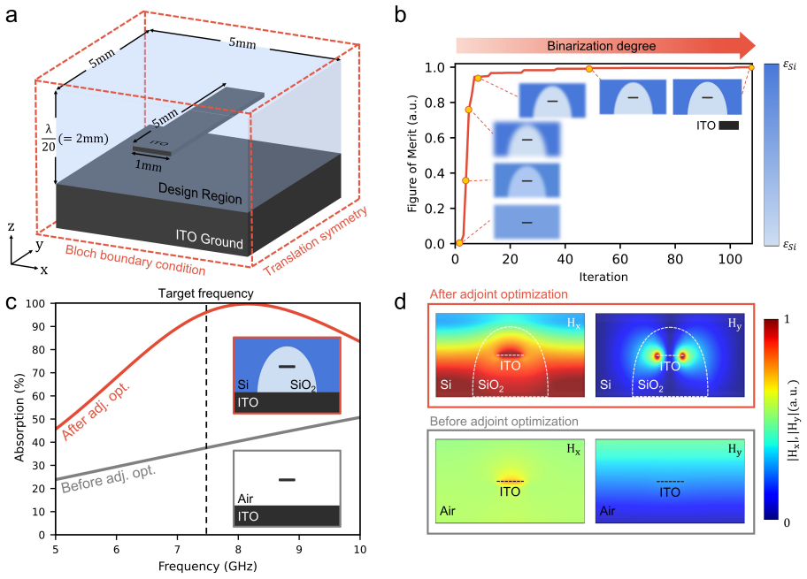
The load-bearing machinery is the adjoint-variable method paired with a magnetic-field figure of merit. In each iteration, one forward simulation and one adjoint simulation give the sensitivity of absorption with respect to every permittivity voxel at once via the reciprocity-based expression $\delta F \approx 2\,\mathrm{Re}\int \mathbf{P}_{\mathrm{ind}}(\mathbf{x}')\cdot \mathbf{H}_{\mathrm{adj}}(\mathbf{x}')\,dV$, where $\mathbf{P}_{\mathrm{ind}}$ is the induced polarization of a small permittivity change and $\mathbf{H}_{\mathrm{adj}}$ is the adjoint magnetic field from dipole sources in the absorbing region. Because the 25-nm ITO film is too thin to grid directly, it is modeled as a one-pixel-thick 125-µm layer with conductivity and permittivity scaled down by 1/5000, following the standard thin-conducting-layer approximation. The optimized silicon/silica pattern that emerges concentrates magnetic fields at the patch edges, producing the resonance that makes the ultrathin stack behave like a thicker Salisbury screen.
What would settle it
Resolve the 25-nm ITO film explicitly, or with a locally refined thin-layer model, in the optimized three-dimensional geometry and compare absorption at 7.5 GHz for 0°, 50°, 60°, and 70° incidence against the scaled 125-µm model. A drop below roughly 90% at normal incidence, or a sharper angular roll-off than the scaled model predicts, would refute the central claim. An experimental alternative is to fabricate the optimized pattern and measure reflection versus angle on a network analyzer.
Extended reading notes
Core claim
Using a figure of merit based on magnetic-field intensity rather than the usual electric-field absorption integral, the authors optimize the arrangement of silicon and silicon dioxide in a 2-mm ($\lambda/20$) dielectric layer around a 25-nm indium tin oxide patch on a conducting ground plane. In a fully three-dimensional periodic simulation, the adjoint-optimized layout absorbs about 91% at 7.5 GHz (peak 92.5% near 7.7 GHz), with a 90%-absorption bandwidth from about 7.4 to 8.2 GHz and robust oblique-incidence behavior: above 90% up to 50°, about 80% at 60°, and about 70% at 70°. The same design in a two-dimensional setup reaches about 95% absorption at the target frequency. The authors attribute the mechanism to strong magnetic-field concentration at the edges of the conductive patch, which excites surface-plasmon-like resonance and lets the thin layer mimic the refractive behavior of a quarter-wave Salisbury screen.
Load-bearing premise
The load-bearing premise is that a 125-micrometer numerical layer whose conductivity and permittivity are scaled down by 1/5000 exactly reproduces the electromagnetic behavior of the real 25-nanometer ITO film inside the optimized three-dimensional structure; the paper validates this equivalence only on a planar stack at normal incidence, not against a resolved simulation of the final design at oblique angles.
Editorial extensions
If this is right
- Absorber thickness can be cut from the conventional $\lambda/4$ to $\lambda/20$ while keeping single-frequency absorption above 90%, relaxing a major geometric constraint for compact military and communications systems.
- Adjoint optimization reaches about 91% absorption at 7.5 GHz in roughly 216 simulations, whereas particle swarm optimization reaches only 56% absorption in 10,800 simulations, meaning a roughly 98% reduction in computational cost for this design problem.
- The optimized design maintains over 90% absorption up to 50° incidence, about 80% at 60°, and about 70% at 70°, so the ultrathin profile does not come at the cost of angular robustness at the target frequency.
- The adjoint-optimized structure has a spatially coherent, layered silicon/silica distribution, in contrast to the disordered pattern from particle swarm optimization, making the final design more plausible to fabricate and test.
- Because adjoint optimization supports multiple objectives, the same framework can be extended to broadband or multi-band absorber designs, as the authors note.
Reading between the lines
- A testable extension is to treat the one-pixel conductivity-scaling trick as a general recipe for atomically thin conducting films in FDTD; checking it against a locally resolved simulation of the final 3D design would show how transferable it is beyond planar validation.
- The paper compares simulation counts rather than wall-clock time including binarization and verification runs; a practical-speed benchmark could narrow the 98% gap, although the 216-versus-10,800 simulation count already indicates a large advantage.
- The magnetic-field figure of merit suggests that maximizing magnetic coupling is the right objective for high-conductivity ultrathin absorbers, so the same formulation could be carried over to other conductor-based metasurface devices such as modulators and sensors.
- A natural frequency-scaling test would be to re-run the optimization at a different target frequency with all dimensions and conductivities scaled proportionally; the paper does not report such a test, and it would clarify whether the angular robustness is a general feature or specific to 7.5 GHz.
Signed reviews
Editorial analysis
A structured set of objections, weighed in public.
Referee Report
Summary. Jang et al. present an inverse-design framework for ultrathin (λ/20) electromagnetic absorbers operating at 7.5 GHz. The core method is adjoint-based topology optimization using a magnetic-field-only figure of merit, applied first to a 2D periodic structure and then to a 3D design with more than 30,000 parameters. The optimized 3D design is reported to absorb 91% at the target frequency, to maintain >90% absorption up to 50° incidence, and to require 216 simulations versus 10,800 for a binary-PSOGSA baseline, i.e., an approximately 98% reduction in computational cost. The final absorption spectra are evaluated independently with FDTD flux monitors, and the paper includes angle-dependent field distributions and a comparison with particle swarm optimization.
Significance. If the claims hold, the paper would demonstrate a practical route to angle-robust ultrathin absorbers with a major reduction in optimization cost, and the reported 98% simulation-count saving is a concrete, checkable quantitative claim. The manuscript has notable strengths: a clearly specified FDTD setup, independent evaluation of the final absorption via flux monitors, a side-by-side comparison with PSO under identical conditions, and an explicit statement of the thin-film scaling approximation. However, the methodological foundations of the adjoint gradient and of the magnetic-field-only objective are not rigorously established, and the ITO subcell model is validated only on a planar stack. These issues are load-bearing for the central efficiency and performance claims, so the significance of the paper depends on repairing them.
major comments (3)
- [Section 2 (equations for δF, H_adj, P_ind, and δF≈2Re∫P_ind·H_adj)] The central gradient formula does not follow from Lorentz reciprocity. A permittivity perturbation acts as an electric polarization current J_p(x′) = −iω(ε2−ε1)E_old(x′), and its first-order contribution to a magnetic-field objective is obtained by contracting J_p with the electric field E_adj generated by the adjoint magnetic dipole source, not by contracting the electric polarization density with the adjoint magnetic field. As written, the integrand P_ind·H_adj has units of C/m² times A/m, which is not an energy density, and no reciprocity identity supporting this pairing is given. Because the claimed 98% computational saving and the attribution of the 91% absorption to adjoint optimization both rest on the gradient being correct, the derivation must be corrected or verified numerically with a finite-difference gradient check on a small design domain.
- [Section 2 and Section 3.2.2] The magnetic-field-only figure of merit is asserted to enhance absorption without a derivation connecting ∫|H|²dV over the ITO region to absorbed power. For a thin conductive film, dissipation is proportional to σ|E_t|², and the relation between |H| and |E_t| is geometry-dependent; it holds for simple transmission-line resonances but not for arbitrary topologies. The paper acknowledges that this basis is 'non-intuitive' but provides no test. Please add a demonstration that the final absorption is monotonic in the FoM along the optimization trajectory, or derive the H-based proxy from the sheet boundary conditions, so the reader can see that the optimized structure is not merely a structure that happens to have high magnetic field.
- [Section 3.1.1] The 125-μm, conductivity- and permittivity-scaled ITO monolayer is validated only against a planar TMM stack. The optimized structure is strongly nonplanar and supports localized field enhancement near the patch edges (Figs. 3d and 7e), and the oblique-incidence claim is exercised up to 70°; the planar validation does not test the model in these regimes. Please add a convergence check with finer ITO models (e.g., 62.5-μm and 31.25-μm scaled layers) in the optimized geometry, or simulate the final design with a thin-sheet boundary condition, to confirm that the reported 91% absorption and angular robustness are not artifacts of the one-pixel approximation.
minor comments (7)
- [Section 3.1.1] The sentence 'ITO (conductivity=0.5×10⁶ S/m, relative permittivity=0.5×10⁶ at 7.5 GHz)' is physically implausible for a real relative permittivity; please clarify the intended constitutive model, e.g., the imaginary part of the permittivity or an effective Drude-model value, and state how both conductivity and permittivity are scaled by the factor 1/5000.
- [Section 3.1.2] The text refers to 'the optimized 2D absorber (described in Section 2.2.1)', but the 2D absorber is described in Section 3.1.1; the cross-reference should be corrected.
- [Fig. 8(b) and Section 3.2.3] The color labels are inconsistent: the Fig. 8(b) caption lists PSO-optimized as red and adjoint-optimized as green, while the Section 3.2.3 text says the PSO-designed absorber is green and the adjoint-optimized absorber is red; please make the colors consistent.
- [Fig. 5 caption] The caption contains the typo 'Three-demensional'; it should read 'Three-dimensional'.
- [Section 4] The phrase 'we have presented a inverse design framework' should be 'an inverse design framework'.
- [Section 3.1.1] The manuscript states that 'the region surrounding the ITO patch is defined as the optimization domain'; please clarify whether the ITO patch itself is fixed during optimization or whether its geometry is also modified, and specify the modeled thickness and material model used for the ground plane.
- [Data availability] The data availability statement is generic; for a computational study with claims of specific percentages (91%, 98%), sharing the optimized geometries and Meep scripts would substantially strengthen reproducibility.
Circularity Check
No significant circularity: the design objective and evaluation frequency coincide by design, while oblique-incidence tests and the PSO comparison provide independent checks.
full rationale
The paper optimizes the absorber for 7.5 GHz and then evaluates absorption at 7.5 GHz; this is the normal inverse-design loop, not a circular prediction, because the optimization target is the stated design goal rather than a fitted parameter relabeled as a discovery. The oblique-incidence performance was not part of the optimization objective and is therefore an independent check of the design's robustness. The comparison with PSO uses identical FDTD settings and reports simulation counts (10,800 vs. 216), so the claimed computational saving is a counting argument rather than a quantity forced by the model. The one-pixel ITO model is validated against a transfer-matrix calculation for the planar stack; even if the approximation is imperfect under oblique or near-field conditions, that is a modeling-accuracy risk, not circularity. Self-citations to prior adjoint-method papers support the methodology, but the adjoint formalism is standard, reproducible with open-source Meep, and no uniqueness theorem from the authors is invoked to forbid alternative designs. The possible reciprocity/units objection to the magnetic-adjoint gradient in Section 2 is a correctness concern about whether the computed gradient is the true FoM gradient; it does not make the reported 91% absorption a restatement of the optimization input. Overall, no load-bearing step reduces, by definition or by self-citation, to its own inputs.
Assumptions & free parameters
free parameters (4)
- Learning rate eta =
not reported
- Binarization factor =
not reported
- Design domain periodicity and patch dimensions =
5 mm periodicity, 1 mm x 1 mm patch
- Exact form of figure-of-merit f(E,H) =
not specified
assumptions (4)
- standard math Lorentz reciprocity and the Born approximation justify the adjoint gradient expression.
- ad hoc to paper The magnetic-field-only figure of merit correctly captures absorption in the high-conductivity ITO film.
- ad hoc to paper The 125-micrometer conductivity-scaled ITO monolayer accurately represents the 25-nanometer ITO film inside the optimized structure.
- domain assumption Bloch boundary conditions in x and y with PML in z accurately model the infinite periodic absorber.
Cite this review
Pith. "Pith review of Inverse design of ultrathin metamaterial absorber." pith.science (2026). https://pith.science/paper/ZDUMW5PM
@misc{pith2026250414901,
  author       = {Pith},
  title        = {Pith review of: Inverse design of ultrathin metamaterial absorber},
  year         = {2026},
  howpublished = {\url{https://pith.science/paper/ZDUMW5PM}},
  note         = {Machine review of arXiv:2504.14901}
}
read the original abstract
Electromagnetic absorbers combining ultrathin profiles with robust absorptivity across wide incidence angles are essential for applications such as stealth technology, wireless communications, and quantum computing. Traditional designs, including Salisbury screens, typically require thicknesses of at least a quarter-wavelength (lambda/4), which limits their use in compact systems. While metamaterial absorbers (MMAs) can reduce thickness, their absorptivity generally decreases under oblique incidence conditions. Here, we introduce an adjoint optimization-based inverse design method that merges the ultrathin advantage of MMAs with the angle-insensitive characteristics of Salisbury screens. By leveraging the computational efficiency of the adjoint method, we systematically optimize absorber structures as thin as lambda/20. The optimized designs achieve absorption exceeding 90% at the target frequency of 7.5 GHz and demonstrate robust performance under oblique incidence, maintaining over 90% absorption up to 50{\deg}, approximately 80% at 60{\deg}, and around 70% at 70{\deg}. Comparative analysis against particle swarm optimization highlights the superior efficiency of the adjoint method, reducing computational effort by approximately 98%. This inverse design framework thus provides substantial improvements in both performance and computational cost, offering a promising approach for advanced electromagnetic absorber design.
Figures


Figures from the paper (5 more)


Reference graph
Works this paper leans on
-
[1]
Metamaterials and negative refractive index,
D. R. Smith, J. B. Pendry, and M. C. Wiltshire, “Metamaterials and negative refractive index,” science 305, 788–792 (2004)
work page 2004
-
[2]
High-na achromatic metalenses by inverse design,
H. Chung and O. D. Miller, “High-na achromatic metalenses by inverse design,” Optics Express 28, 6945–6965 (2020)
work page 2020
-
[3]
Topology optimization of freeform large-area metasurfaces,
Z. Lin, V . Liu, R. Pestourie, and S. G. Johnson, “Topology optimization of freeform large-area metasurfaces,” Optics express27, 15765–15775 (2019)
work page 2019
-
[4]
High-efficiency, large-area, topology-optimized metasurfaces,
T. Phan, D. Sell, E. W. Wang, S. Doshay, K. Edee, J. Yang, and J. A. Fan, “High-efficiency, large-area, topology-optimized metasurfaces,” Light: Science & Applications 8, 48 (2019)
work page 2019
-
[5]
Deep-learning-driven end-to-end metalens imaging,
J. Seo, J. Jo, J. Kim, J. Kang, C. Kang, S.-W. Moon, E. Lee, J. Hong, J. Rho, and H. Chung, “Deep-learning-driven end-to-end metalens imaging,” Advanced Photonics 6, 066002–066002 (2024)
work page 2024
-
[6]
C. Kang, J. Seo, I. Jang, and H. Chung, “Adjoint method-based fourier neural operator surrogate solver for wavefront shaping in tunable metasurfaces,” iScience 28 (2025)
work page 2025
-
[7]
Information metasurface for electromagnetic sensing and wireless communications,
X. Wan, Z. A. Huang, J. W. Wang, W. H. Wang, B. Y . Li, Q. Xiao, X. J. Wang, J. C. Wan, and T. J. Cui, “Information metasurface for electromagnetic sensing and wireless communications,” Advanced Materials Technologies9, 2301629 (2024)
work page 2024
-
[8]
Y . Wang, C. Zhao, J. Wang, X. Luo, L. Xie, S. Zhan, J. Kim, X. Wang, X. Liu, and Y . Ying, “Wearable plasmonic-metasurface sensor for noninvasive and universal molecular fingerprint detection on biointerfaces,” Science Advances7, eabe4553 (2021)
work page 2021
Show all 73 references
-
[9]
Broadband surface enhanced infrared absorption with multiple fano resonance by metallic oblique-wire-bundle metamaterial absorbers,
H.-S. Lee, Y .-P. Kuang, C.-Y . Lu, T.-J. Yen, and T.-Y . Huang, “Broadband surface enhanced infrared absorption with multiple fano resonance by metallic oblique-wire-bundle metamaterial absorbers,” Scientific Reports 14, 27328 (2024)
2024
-
[10]
Large-area metasurface perfect absorbers from visible to near-infrared,
G. M. Akselrod, J. Huang, T. B. Hoang, P. T. Bowen, L. Su, D. R. Smith, and M. H. Mikkelsen, “Large-area metasurface perfect absorbers from visible to near-infrared,” Advanced Materials 27, 8028–8034 (2015)
2015
-
[11]
Optically transparent ultrawideband electromagnetic stealth metasurface for microwave absorption and scattering,
Y . Ran, L. Shi, S. Wu, J. Li, X. Jin, Z. Hou, B. Fan, and J. Wang, “Optically transparent ultrawideband electromagnetic stealth metasurface for microwave absorption and scattering,” IEEE Antennas and Wireless Propagation Letters21, 2412–2416 (2022)
2022
-
[12]
Light-emitting metasurfaces,
A. Vaskin, R. Kolkowski, A. F. Koenderink, and I. Staude, “Light-emitting metasurfaces,” Nanophotonics 8, 1151–1198 (2019)
2019
-
[13]
Enhanced light extraction from organic light-emitting diodes with micro-nano hybrid structure,
E.-J. Bae, S.-W. Kang, G.-S. Choi, E.-B. Jang, D.-H. Baek, B.-K. Ju, and Y .-W. Park, “Enhanced light extraction from organic light-emitting diodes with micro-nano hybrid structure,” Nanomaterials 12, 1266 (2022)
2022
-
[14]
A simple method for fabricating an external light extraction composite layer with rns to improve the optical properties of oleds,
G.-S. Choi, S.-W. Kang, E.-J. Bae, E.-B. Jang, D.-H. Baek, B.-K. Ju, and Y .-W. Park, “A simple method for fabricating an external light extraction composite layer with rns to improve the optical properties of oleds,” Nanomaterials 12, 1430 (2022)
2022
-
[15]
Chiral plasmonic metasurface assembled by dna origami,
N. Gieseler, S. Moench, D. Beutel, W. G. Pfeifer, C. M. Domínguez, C. M. Niemeyer, and C. Rockstuhl, “Chiral plasmonic metasurface assembled by dna origami,” Optics Express 32, 16040–16051 (2024)
2024
-
[16]
Nonlinear optical encoding enabled by recurrent linear scattering,
F. Xia, K. Kim, Y . Eliezer, S. Han, L. Shaughnessy, S. Gigan, and H. Cao, “Nonlinear optical encoding enabled by recurrent linear scattering,” Nature Photonics 18, 1067–1075 (2024)
2024
-
[17]
Hyperspectral in-memory computing with optical frequency combs and pro- grammable optical memories,
M. H. Latifpour, B. J. Park, Y . Yamamoto, and M.-G. Suh, “Hyperspectral in-memory computing with optical frequency combs and pro- grammable optical memories,” Optica 11, 932–939 (2024)
2024
-
[18]
Flat-knit, flexible, textile metasurfaces,
M. J. Carter, L. Resneck, Y . Ra’di, and N. Yu, “Flat-knit, flexible, textile metasurfaces,” Advanced Materials 36, 2312087 (2024)
2024
-
[19]
Metasurfaces for near-eye display applications,
Y . Li, X. Huang, S. Liu, H. Liang, Y . Ling, and Y . Su, “Metasurfaces for near-eye display applications,” Opto-Electronic Science2, 230025–1 (2023)
2023
-
[20]
Dual-channel near-field holographic mimo communications based on programmable digital coding metasurface and electromagnetic theory,
R. W. Shao, J. W. Wu, J. Li, S. Meng, Y . Xu, Z. X. Wang, W. Tang, Q. Cheng, S. Jin, and T. J. Cui, “Dual-channel near-field holographic mimo communications based on programmable digital coding metasurface and electromagnetic theory,” Nature Communications 16, 915 (2025)
2025
-
[21]
Perfect metamaterial absorber,
N. I. Landy, S. Sajuyigbe, J. J. Mock, D. R. Smith, and W. J. Padilla, “Perfect metamaterial absorber,” Physical review letters 100, 207402 (2008)
2008
-
[22]
Metamaterial electromagnetic wave absorbers,
C. M. Watts, X. Liu, and W. J. Padilla, “Metamaterial electromagnetic wave absorbers,” Advanced materials 24, OP98–OP120 (2012)
2012
-
[23]
Reflection properties of the salisbury screen,
R. L. Fante and M. T. McCormack, “Reflection properties of the salisbury screen,” IEEE transactions on antennas and propagation 36, 1443– 1454 (1988)
1988
-
[24]
Selective dual-band metamaterial perfect absorber for infrared stealth technology,
J. Kim, K. Han, and J. W. Hahn, “Selective dual-band metamaterial perfect absorber for infrared stealth technology,” Scientific reports7, 6740 (2017)
2017
-
[25]
Broadband metamaterial absorber for stealth applications at k-band,
L. Dewangan, M. S. Patinavalasa, J. Acharjee, Y . Solunke, S. Ghosh, and N. K. Mishra, “Broadband metamaterial absorber for stealth applications at k-band,” AEU-International Journal of Electronics and Communications 170, 154828 (2023)
2023
-
[26]
Absorbent body for electromagnetic waves,
W. W. Salisbury, “Absorbent body for electromagnetic waves,” (1952)
1952
-
[27]
The design of jauman absorbers,
L. J. Du Toit, “The design of jauman absorbers,” IEEE Antennas and Propagation Magazine 36, 17–25 (1994)
1994
-
[28]
Ultimate thickness to bandwidth ratio of radar absorbers,
K. N. Rozanov, “Ultimate thickness to bandwidth ratio of radar absorbers,” IEEE Transactions on Antennas and Propagation 48, 1230–1234 (2000)
2000
-
[29]
Multispectral flexible ultrawideband metamaterial absorbers for radar stealth and visible light transparency,
J. Kang, Z. Qu, J. Duan, H. Jing, J. Hao, C. Song, J. Wang, and B. Zhang, “Multispectral flexible ultrawideband metamaterial absorbers for radar stealth and visible light transparency,” Optical Materials135, 113351 (2023)
2023
-
[30]
Transparent ultra-broadband absorber based on a tree seedling composite structure,
Z. Lyu, B. Zhang, J. Duan, Y . Yang, R. Liu, Y . Wei, and J. Liu, “Transparent ultra-broadband absorber based on a tree seedling composite structure,” Journal of Physics D: Applied Physics 55, 095104 (2021)
2021
-
[31]
An ultra-broadband and optically transparent metamaterial absorber based on multilayer indium-tin-oxide structure,
G. Deng, K. Lv, H. Sun, J. Yang, Z. Yin, B. Chi, and X. Li, “An ultra-broadband and optically transparent metamaterial absorber based on multilayer indium-tin-oxide structure,” Journal of Physics D: Applied Physics 54, 165301 (2021)
2021
-
[32]
Inverse design of diffusion–absorption hybrid metasur- faces,
Z. Song, R. Zhang, P. Min, T. Wang, W. Cao, Y . He, L. Wu, J. Zhu, and C.-W. Qiu, “Inverse design of diffusion–absorption hybrid metasur- faces,” Laser & Photonics Reviews 17, 2300280 (2023)
2023
-
[33]
Freeform thin-film lithium niobate mode converter for photon-pair generation,
C. Kim, M. Bae, M. Choi, S. Lee, M. Lee, C. Kim, H. Jung, H. Chung, and H. Kwon, “Freeform thin-film lithium niobate mode converter for photon-pair generation,” Nanophotonics (2025)
2025
-
[34]
Large-scale parametrized metasurface design using adjoint optimization,
M. Mansouree, A. McClung, S. Samudrala, and A. Arbabi, “Large-scale parametrized metasurface design using adjoint optimization,” Acs Photonics 8, 455–463 (2021)
2021
-
[35]
Large-scale photonic inverse design: computational challenges and break- throughs,
C. Kang, C. Park, M. Lee, J. Kang, M. S. Jang, and H. Chung, “Large-scale photonic inverse design: computational challenges and break- throughs,” Nanophotonics 13, 3765–3792 (2024)
2024
-
[36]
Particle swarm optimization,
J. Kennedy and R. Eberhart, “Particle swarm optimization,” in Proceedings of ICNN’95-international Conference on Neural Networks, V ol. 4 (IEEE, 1995) pp. 1942–1948
1995
-
[37]
Particle swarm optimization: technique, system and challenges,
D. P. Rini, S. M. Shamsuddin, and S. S. Yuhaniz, “Particle swarm optimization: technique, system and challenges,” International journal of computer applications 14, 19–26 (2011)
2011
-
[38]
Gaga for nonreciprocal emitters: genetic algorithm gradient ascent optimization of compact magnetophotonic crystals,
H. Gold, S. Pajovic, A. Mukherjee, and S. V . Boriskina, “Gaga for nonreciprocal emitters: genetic algorithm gradient ascent optimization of compact magnetophotonic crystals,” Nanophotonics 13, 773–792 (2024)
2024
-
[39]
Tunable metasurface inverse design for 80% switching efficiencies and 144 angular deflection,
H. Chung and O. D. Miller, “Tunable metasurface inverse design for 80% switching efficiencies and 144 angular deflection,” ACS Photonics 7, 2236–2243 (2020)
2020
-
[40]
Low-frequency tunable acoustic absorber based on split tube resonators,
X. Wu, C. Fu, X. Li, Y . Meng, Y . Gao, J. Tian, L. Wang, Y . Huang, Z. Yang, and W. Wen, “Low-frequency tunable acoustic absorber based on split tube resonators,” Applied Physics Letters 109 (2016)
2016
-
[41]
A wide incident angle, ultrathin, polarization-insensitive metamaterial absorber for optical wavelength applications,
S. Mahmud, S. S. Islam, A. F. Almutairi, and M. T. Islam, “A wide incident angle, ultrathin, polarization-insensitive metamaterial absorber for optical wavelength applications,” Ieee Access 8, 129525–129541 (2020)
2020
-
[42]
Genetic algorithms,
J. H. Holland, “Genetic algorithms,” Scientific American 267, 66–73 (1992)
1992
-
[43]
Miller, Photonic Design: From Fundamental Solar Cell Physics to Computational Inverse Design , Ph.D
O. Miller, Photonic Design: From Fundamental Solar Cell Physics to Computational Inverse Design , Ph.D. thesis, EECS Department, Uni- versity of California, Berkeley (2012)
2012
-
[44]
Efficient adjoint-based shape optimization method for the inverse design of microwave compo- nents,
S. Ji, S. HuYan, L. Du, X. Xu, and J. Zhao, “Efficient adjoint-based shape optimization method for the inverse design of microwave compo- nents,” IEEE Transactions on Microwave Theory and Techniques (2024)
2024
-
[45]
Giga-voxel computational morphogenesis for structural design,
N. Aage, E. Andreassen, B. S. Lazarov, and O. Sigmund, “Giga-voxel computational morphogenesis for structural design,” Nature 550, 84–86 (2017)
2017
-
[46]
Fundamental limits to optical response in absorptive systems,
O. D. Miller, A. G. Polimeridis, M. Homer Reid, C. W. Hsu, B. G. DeLacy, J. D. Joannopoulos, M. Soljaˇci´c, and S. G. Johnson, “Fundamental limits to optical response in absorptive systems,” Optics express 24, 3329–3364 (2016)
2016
-
[47]
J. D. Jackson, Classical electrodynamics (John Wiley & Sons, 1998)
1998
-
[48]
A. H. Sihvola, Electromagnetic mixing formulas and applications, 47 (Iet, 1999)
1999
-
[49]
Adjoint method in machine learning: A pathway to efficient inverse design of photonic devices,
C. Kang, D. Seo, S. V . Boriskina, and H. Chung, “Adjoint method in machine learning: A pathway to efficient inverse design of photonic devices,” Materials & Design 239, 112737 (2024)
2024
-
[50]
Inverse design and optical vortex manipulation for thin-film absorption enhancement,
M. Bae, J. Jo, M. Lee, J. Kang, S. V . Boriskina, and H. Chung, “Inverse design and optical vortex manipulation for thin-film absorption enhancement,” Nanophotonics 12, 4239–4254 (2023)
2023
-
[51]
Electromagnetic microwave absorption theory and recent achievements in microwave absorbers,
X. Zeng, X. Cheng, R. Yu, and G. D. Stucky, “Electromagnetic microwave absorption theory and recent achievements in microwave absorbers,” Carbon 168, 606–623 (2020)
2020
-
[52]
Meep: A flexible free-software package for electromagnetic simulations by the fdtd method,
A. F. Oskooi, D. Roundy, M. Ibanescu, P. Bermel, J. D. Joannopoulos, and S. G. Johnson, “Meep: A flexible free-software package for electromagnetic simulations by the fdtd method,” Computer Physics Communications 181, 687–702 (2010)
2010
-
[53]
Indium tin oxide film characterization at 0.1–20 ghz using coaxial probe method,
E. A. Alwan, A. Kiourti, and J. L. V olakis, “Indium tin oxide film characterization at 0.1–20 ghz using coaxial probe method,” IEEE access3, 648–652 (2015)
2015
-
[54]
The electronic properties of graphene,
A. H. Castro Neto, F. Guinea, N. M. Peres, K. S. Novoselov, and A. K. Geim, “The electronic properties of graphene,” Reviews of modern physics 81, 109–162 (2009)
2009
-
[55]
Efficient 3d simulation of thin conducting layers of arbitrary thickness,
G. Eriksson, “Efficient 3d simulation of thin conducting layers of arbitrary thickness,” in 2007 IEEE International Symposium on Electromag- netic Compatibility (IEEE, 2007) pp. 1–6
2007
-
[56]
M. P. Bendsoe and O. Sigmund, Topology optimization: theory, methods, and applications (Springer Science & Business Media, 2013)
2013
-
[57]
Inverse design of chiral structures for giant helical dichroism,
C.-C. Pan, M. Bae, H. Wang, J. Lim, R. R. Unnithan, J. Yang, H. Chung, and S. Kim, “Inverse design of chiral structures for giant helical dichroism,” arXiv preprint arXiv:2501.12825 (2025)
2025 arXiv
-
[58]
Binary optimization using hybrid particle swarm optimization and gravitational search algorithm,
S. Mirjalili, G.-G. Wang, and L. d. S. Coelho, “Binary optimization using hybrid particle swarm optimization and gravitational search algorithm,” Neural Computing and Applications 25, 1423–1435 (2014)
2014
-
[59]
Flexible metamaterial absorbers for stealth applications at terahertz frequencies,
K. Iwaszczuk, A. C. Strikwerda, K. Fan, X. Zhang, R. D. Averitt, and P. U. Jepsen, “Flexible metamaterial absorbers for stealth applications at terahertz frequencies,” Optics express 20, 635–643 (2011)
2011
-
[60]
Triple band microwave metamaterial absorber based on double e-shaped symmetric split ring resonators for emi shielding and stealth applications,
M. B. Hossain, M. R. I. Faruque, M. T. Islam, M. Singh, and M. Jusoh, “Triple band microwave metamaterial absorber based on double e-shaped symmetric split ring resonators for emi shielding and stealth applications,” Journal of Materials Research and Technology18, 1653– 1668 (2022)
2022
-
[61]
Microwave energy harvesting based on metamaterial absorbers with multi- layered square split rings for wireless communications,
M. Karaaslan, M. Ba ˘gmancı, E. Ünal, O. Akgol, and C. Sabah, “Microwave energy harvesting based on metamaterial absorbers with multi- layered square split rings for wireless communications,” Optics Communications 392, 31–38 (2017)
2017
-
[62]
Simulation of the microwave five-band a perfect metamaterial absorber for the 5g communication,
S. A. Mohammed, R. A. K. Albadri, and K. S. L. Al-Badri, “Simulation of the microwave five-band a perfect metamaterial absorber for the 5g communication,” Heliyon 9 (2023)
2023
-
[63]
Trapping of single atoms in metasurface optical tweezer arrays,
A. Holman, Y . Xu, X. Sun, J. Wu, M. Wang, B. Seo, N. Yu, and S. Will, “Trapping of single atoms in metasurface optical tweezer arrays,” arXiv preprint arXiv:2411.05321 (2024)
2024
-
[64]
Computational upper-limit of directional light emission in nano-led via inverse design,
H. Chung, “Computational upper-limit of directional light emission in nano-led via inverse design,” Optics Express 30, 9008–9020 (2022)
2022
-
[65]
Many photonic design problems are sparse qcqps,
S. Gertler, Z. Kuang, C. Christie, H. Li, and O. D. Miller, “Many photonic design problems are sparse qcqps,” Science Advances 11, eadl3237 (2025)
2025
-
[66]
Computational electromagnetics: the finite-difference time-domain method,
A. Taflove, S. C. Hagness, and M. Piket-May, “Computational electromagnetics: the finite-difference time-domain method,” The Electrical Engineering Handbook 3, 15 (2005)
2005
-
[67]
K. S. Kunz and R. J. Luebbers, The finite difference time domain method for electromagnetics (CRC press, 1993)
1993
-
[68]
Effect of film thickness on the properties of indium tin oxide thin films,
H. Kim, J. Horwitz, G. Kushto, A. Pique, Z. Kafafi, C. Gilmore, and D. Chrisey, “Effect of film thickness on the properties of indium tin oxide thin films,” Journal of applied physics 88, 6021–6025 (2000)
2000
-
[69]
P. R. Gray, P. J. Hurst, S. H. Lewis, and R. G. Meyer, Analysis and design of analog integrated circuits (John Wiley & Sons, 2024)
2024
-
[70]
Semiconductor materials and process technology handbook: for very large scale integration (vlsi) and ultra large scale integration (ulsi),
G. E. McGuire, “Semiconductor materials and process technology handbook: for very large scale integration (vlsi) and ultra large scale integration (ulsi),” Electronics Reliability and Measurement Technology , ibc2 (1988)
1988
-
[71]
Characterization and structural property of indium tin oxide thin films,
E. Parsianpour, D. Raoufi, M. Roostaei, B. Sohrabi, and F. Samavat, “Characterization and structural property of indium tin oxide thin films,” Advances in Materials Physics and Chemistry 7, 42–57 (2017)
2017
-
[72]
A class of globally convergent optimization methods based on conservative convex separable approximations,
K. Svanberg, “A class of globally convergent optimization methods based on conservative convex separable approximations,” SIAM journal on optimization 12, 555–573 (2002)
2002
-
[73]
The NLopt nonlinear-optimization package,
S. G. Johnson, “The NLopt nonlinear-optimization package,” https://github.com/stevengj/nlopt (2007)
2007
Reviewed August 16, 2026 · model on record in the stance chip above.
Discussion (0). Continue with ORCID to comment.