REVIEW 2 major objections 5 minor 2 cited by
Modelling the Impact of Device Imperfections on Electron Shuttling in SiMOS devices
T0 review · 2 major / 5 minor · reviewed 2026-08-03 · deepseek-v4-flash
Pith's one-line read Conveyor-belt electron shuttling in silicon-oxide devices is robust above a clavier-gate voltage of about 150 mV, but positively charged interface defects can permanently capture the electron at lower voltages.
desk verdict Solid, useful 3D shuttling simulations with a believable low-voltage mode transition; the permanent-capture claim for positive defects rests on a static-charge model the paper itself contradicts. read the letter →
The pith
A machine-rendered reading of the paper's core claim, the machinery that carries it, and where it could break.
The reading
What carries the argument
The key machinery is the instantaneous eigenenergy spectrum of the moving dot, analysed through the Landau–Zener formula P_D = exp(-2π a²/(ℏ|α|)), where a is the gap between neighbouring orbital levels and α the sweep rate. The paper shows how the multi-layer gate stack's uneven screening shrinks a under alternating gates at low voltage, driving the shuttling through avoided crossings and into a bucket-brigade mode; this same gap analysis explains robustness at higher voltage and the trapping by positive defects, whose bound states sit deep below the conveyor levels. On the simulation side, the spectral projection method propagates the wavefunction by projecting onto the instantaneous eigenb
What would settle it
Measure shuttling fidelity across a single SiMOS device with a deliberately placed or identified positive interface trap while sweeping the clavier voltage; if at Vc ≈ 100 mV the electron does not remain trapped for the remainder of the cycle (e.g., escapes after the trap neutralises), the fixed-charge capture scenario is refuted. Alternatively, a self-consistent Schrödinger-Poisson simulation with occupation-dependent trap charge would show capture without permanent trapping.
Extended reading notes
Core claim
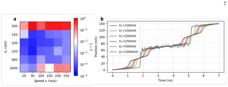
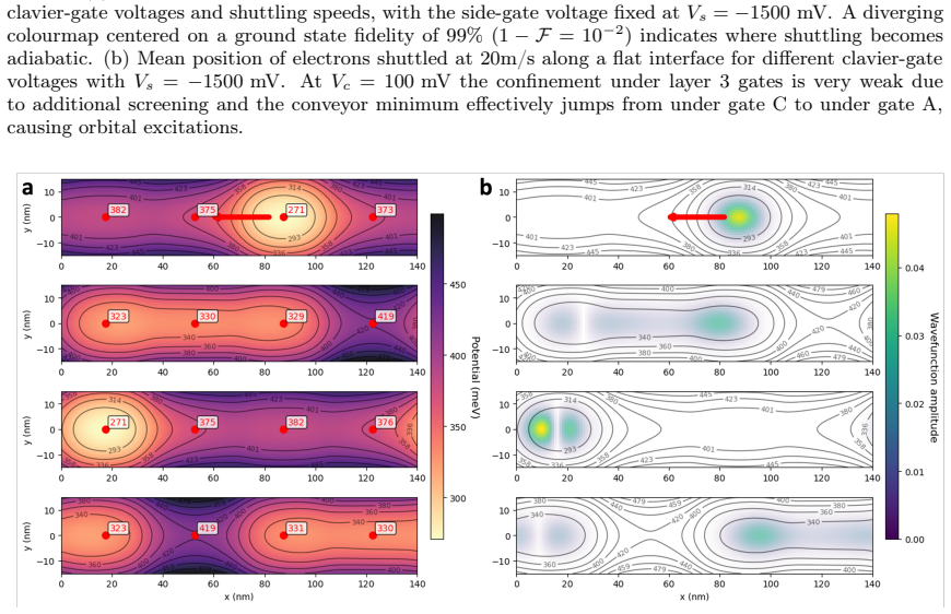
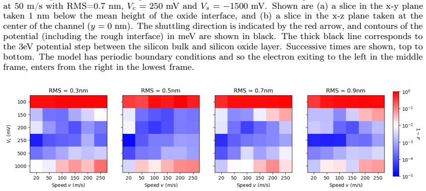
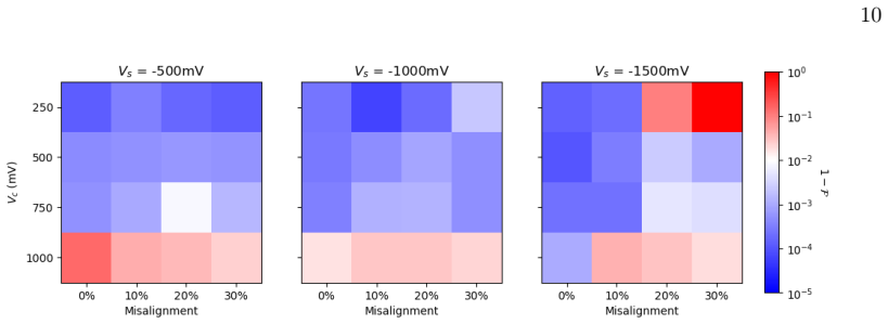
The central claim is that the viability of conveyor-belt electron shuttling in SiMOS devices is governed by a sharp voltage threshold set by the multi-layer gate stack. Because the clavier gates sit in two different oxide layers, the lower-layer gates are screened more heavily; below about 100 mV this creates barriers under alternating gates, and the electron hops rather than rides, suffering large orbital excitation. Raising the clavier voltage above roughly 150 mV re-opens the orbital energy gaps and makes the transport adiabatic and loss-free, with ground-state fidelities above 99% for interface roughness up to 0.9 nm RMS and gate misalignments up to 30%. Negatively charged defects only d
Load-bearing premise
The simulations treat every defect as a point charge of fixed magnitude +e or -e whose charge does not change when it absorbs or emits an electron; if real interface traps neutralise upon capturing an electron, the predicted permanent capture and worst-case excitation results could be substantially weaker.
Editorial extensions
If this is right
- SiMOS conveyor-belt shuttling should be operated with clavier-gate voltages above about 150 mV (and below the very high range where excessive confinement causes excitation) to remain adiabatic.
- Interface roughness and gate misalignment at realistic levels (RMS ≤ 0.9 nm; misalignment ≤ 30%) do not break shuttling, so fabrication tolerances can be looser than feared.
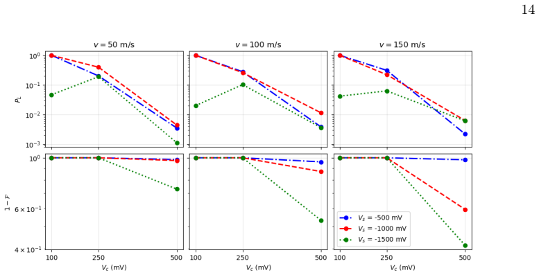
- Positively charged interface defects are the primary showstopper: at low bias they can permanently trap the electron, so device designs or passivation processes should target donor-like interface traps.
- Negatively charged defects are comparatively benign at proper operating voltages, causing negligible charge loss and fidelities of roughly 99–99.99%.
- Even when the electron escapes a positive defect, the resulting orbital excitation may open spin-flip channels, but the small spin-orbit admixture (≈10⁻³) keeps spin-conserving decay dominant.
Reading between the lines
- If the fixed-charge assumption were relaxed, the permanent-capture conclusion could weaken: real Si/SiO2 interface traps (Pb centers) are amphoteric and would neutralise after capturing an electron, potentially releasing it and restoring shuttling.
- The sharp fidelity drop at the conveyor-belt–bucket-brigade transition could serve as a sensitive experimental probe of the effective screening depth in the gate stack, without requiring single-defect resolution.
- The voltage-window result suggests a practical tuning strategy: sweep the clavier voltage while measuring shuttling fidelity to locate the onset above ~150 mV and to detect strong positive traps via the capture signature.
- The orbital-only model sets a necessary-but-not-sufficient condition for spin qubit transport; adding spin and valley dynamics would test whether the identified safe windows survive phonon-mediated spin relaxation in the excited orbitals.
Editorial analysis
A structured set of objections, weighed in public.
Referee Report
Summary. This paper presents full 3D simulations of conveyor-belt electron shuttling in a SiMOS device, solving the Poisson equation for the gate-induced potential and the time-dependent Schrödinger equation for the electron. The authors study the effect of clavier-gate voltage, shuttling speed, interface roughness, gate misalignment, and isolated charge defects. Their central findings are: (i) at low clavier voltage (~100 mV), the multilayer gate geometry causes a transition from conveyor-belt to bucket-brigade shuttling with strong orbital excitation; (ii) raising the voltage above ~150 mV restores conveyor-belt operation, which is robust to realistic interface roughness and gate misalignment; and (iii) positive charge defects at the Si/SiO2 interface are the dominant obstacle, capable of permanently capturing the electron at low voltages. The numerical method is a spectral projection scheme validated against split-operator evolution, and the model parameters are taken from prior literature rather than fitted.
Significance. If the conclusions hold, the paper provides a valuable design-oriented map of operating regimes for SiMOS shuttling, a topic where experiments are still emerging. The study's strengths are the full 3D treatment, the absence of fitted parameters targeting the results, the clear benchmark of the spectral projection method (Appendix B2d), and the systematic parameter sweeps. However, the most distinctive claim—that positive interface defects can permanently trap the shuttled electron—rests on a fixed point-charge defect model that is in tension with the amphoteric Pb-center physics described in the paper's own introduction. Because this issue directly affects the headline threat ranking, the central conclusion is not yet secure without additional analysis or a explicit limitation-aware bounding study.
major comments (2)
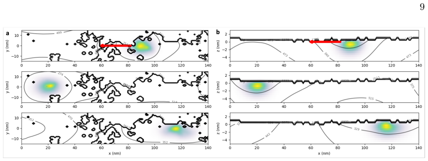
- [Sec. II.C, Eq. (5); Sec. III.D.2, Fig. 13] The positive-defect simulations model each defect as a fixed point charge q=+e. The introduction states that interface traps are amphoteric Pb0/Pb1 centers whose charge state depends on occupancy. Under this physical picture, a +e trap that captures the shuttled electron should neutralize or at least change its charge state, removing the ~200 meV static well that is invoked to explain 'permanent' trapping. The reported permanent capture and the ranking 'positive defects are the greatest obstacle' may therefore be an artifact of the frozen charge state. A concrete bounding test is needed—for example, turning off the trap charge after the first capture event, or using an occupation-dependent defect charge—and the resulting changes in PL and fidelity should be reported. Without such a test, the central conclusion of Sec. III.D.2 is not supported.
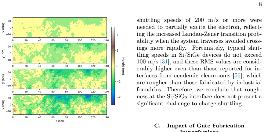
- [Sec. III.B, Figs. 4 and 6] The roughness study appears to use a single stochastically generated interface realization per RMS value. Since interface roughness is a random field, a single realization cannot support quantitative statements such as 'ground state fidelities stay above 99% even with roughness as high as RMS=0.9 nm'. The authors should either average over an ensemble of roughness realizations for each RMS or state explicitly that the reported results are single-sample evidence. This is important because the robustness claim for roughness is a central positive result of the paper.
minor comments (5)
- [Fig. 14 caption] The caption says 'Vs = 500mV', 'Vs = 250mV', and 'Vs = 100mV' in the three panels; these should be Vc (clavier voltage) for consistency with the text.
- [Fig. 4 caption] The cross-reference 'Fig. Ie' should be 'Fig. 1e'.
- [Sec. II.D and Appendix B2b] 'Lanzcos' is a misspelling of 'Lanczos'. Also, the effective-mass tensor notation in Eq. (9) could be clarified by explicitly defining m_t and m_l immediately after the equation.
- [Sec. III.D.2 and Sec. IV] The word 'excitement' is used where 'excitation' is intended in several places (e.g., 'only minor excitement occurs').
- [Eq. (12) and Appendix A] The Landau-Zener formula is used repeatedly but no reference or derivation is given for the specific form with exponent a^2/(ℏ|α|). A brief citation or a note on the sign convention for α would help the reader.
Circularity Check
No significant circularity: the central claims emerge from solving the stated 3D Poisson + time-dependent Schrödinger equations with independently sourced parameters; the one overlapping-author citation is contextual, not load-bearing.
full rationale
The paper's predictions are outputs of a well-specified numerical model, not identities with its inputs. The potential is assembled from stated ingredients: the gate voltages of Eq. (1), the oxide barrier of Eq. (6), and point-charge defects of Eq. (5); the dynamics are then computed with the Schrödinger equation, Eqs. (8)-(9). The swept parameters Vc, Vs, and v are independent control variables, and no parameter is fitted to the reported fidelities, charge-loss probabilities, or the Vc ≈ 100 mV conveyor-to-bucket-brigade transition. The Landau-Zener formula, Eq. (12), is used after the fact to interpret the observed avoided crossings and is not used to set the thresholds. The numerical solver is independently validated against a split-operator Trotter benchmark (Appendix B2d, Fig. 15) and its equivalence to exact Schrödinger evolution is derived in Appendix C, so the spectral projection method is not circularly relied upon. The only overlapping-author citation is [16] (Jeon, Benjamin, Fisher), which is cited as prior 2D context; the present paper independently simulates negative defects in 3D in Sec. III.D.1, so that citation is not load-bearing. The fixed +e point-charge trap model, Sec. II.C and Eq. (5), is a physical simplification that may affect the correctness of the permanent-capture claim, but that is a modelling assumption and a correctness risk, not a circularity: the conclusion is not definitionally identical to the input but is a computed consequence of that stated assumption.
Assumptions & free parameters
free parameters (4)
- Hurst coefficient H =
0.3
- Si/SiO2 conduction-band offset =
3000 meV
- Roughness correlation length / PSD cutoffs =
not stated
- Gate-stack geometry (oxide spacings) =
15 nm under side-gates, 5 nm inter-layer
assumptions (6)
- domain assumption Anisotropic single-valley effective-mass Hamiltonian (Eq. 9) with mt=0.190me and ml=0.916me captures the electron dynamics
- domain assumption Defects are static point charges ±e entering only through Vch in Eq. (5); no charge-state dynamics and no dynamical screening
- domain assumption The electron exerts no back-action on the potential: one-way coupling of the Poisson solution into the Schrödinger dynamics
- domain assumption Periodic boundary conditions in the shuttling direction
- standard math Landau-Zener formula PD=exp(-2πΓ) (Eq. 12) governs excitation probabilities at avoided crossings
- domain assumption The multi-layer gate stack with 5 nm extra oxide under layer-3 gates is representative of realistic SiMOS fabrication
Cite this review
Pith. "Pith review of Modelling the Impact of Device Imperfections on Electron Shuttling in SiMOS devices." pith.science (2026). https://pith.science/paper/HFTPFD26
@misc{pith2026251203853,
  author       = {Pith},
  title        = {Pith review of: Modelling the Impact of Device Imperfections on Electron Shuttling in SiMOS devices},
  year         = {2026},
  howpublished = {\url{https://pith.science/paper/HFTPFD26}},
  note         = {Machine review of arXiv:2512.03853}
}
read the original abstract
Extensive theoretical and experimental work has established high-fidelity electron shuttling in Si/SiGe systems, whereas demonstrations in Si/SiO2 (SiMOS) remain at an early stage. To help address this, we perform full 3D simulations of conveyor-belt charge shuttling in a realistic SiMOS device, building on earlier 2D modelling. We solve the Poisson and time-dependent Schrodinger equations for varying shuttling speeds and gate voltages, focusing on potential pitfalls of typical SiMOS devices such as oxide-interface roughness, gate fabrication imperfections, and charge defects along the transport path. The simulations reveal that for low clavier-gate voltages, the additional oxide screening in multi-layer gate architectures causes conveyor-belt shuttling to collapse to the bucket-brigade mode, inducing considerable orbital excitation in the process. Increasing the confinement restores conveyor-belt operation, which we find to be robust against interface roughness, gate misalignment, and charge defects buried in the oxide. However, our results indicate that defects located at the Si/SiO2-interface can induce considerable orbital excitation. For lower conveyor gate biases, positive defects in the transport channel can even capture passing electrons. Hence we identify key challenges and find operating regimes for reliable charge transport in SiMOS architectures.
Figures

Figures from the paper (10 more)




Forward citations
Cited by 2 Pith papers
-
Electron shuttling as a probe for charge defects
A shuttled electron's spin-dephasing pattern as a function of shuttle distance reveals the position and dynamics of individual charge defects in silicon.
-
Nanostructure modelling with early fault tolerant quantum computers
Quantum simulation framework for ground-state energies of 4- and 8-electron double quantum dots on surface-code fault-tolerant hardware, with resource estimates of 226k-314k physical qubits and 24 hours to 3.4 days ru...
Reference graph
Works this paper leans on
-
[1]
This effect is more pronounced for high side-gate voltages where the dot is more elongated
Negative Charge Defects A negatively charged defect acts similarly to the barrier gate in a double quantum dot sys- tem, with the Coulomb repulsion forming a re- gion of high potential in the channel. This effect is more pronounced for high side-gate voltages where the dot is more elongated. For the position sweep, we place the nega- tive defect at sixtee...
-
[2]
Our simulations show that the electron is per- manently trapped at this site in extreme cases where the conveyor confinement is weak and the defect is located at the interface
Positive Charge Defects In contrast to negative defects, a single pos- itively charged defect introduces an attractive potential for the electron that effectively creates an additional site for quantum dot formation. Our simulations show that the electron is per- manently trapped at this site in extreme cases where the conveyor confinement is weak and the...
-
[3]
A. M. J. Zwerver, T. Krähenmann, T. F. Wat- son, L. Lampert, H. C. George, R. Pillarisetty, S. A. Bojarski, P. Amin, S. V. Amitonov, J. M. Boter, R. Caudillo, D. Correas-Serrano, J. P. Dehollain, G. Droulers, E. M. Henry, R. Kotlyar, M. Lodari, F. Lüthi, D. J. Micha- lak, B. K. Mueller, S. Neyens, J. Roberts, N. Samkharadze, G. Zheng, O. K. Zietz, G. Scap...
2022
-
[4]
Tyryshkin, Shinichi Tojo, John J
Alexei M. Tyryshkin, Shinichi Tojo, John J. L. Morton, Helge Riemann, Nikolai V. Abrosimov, Peter Becker, Hans-Joachim Pohl, Thomas Schenkel, Michael L. W. Thewalt, Ko- hei M. Itoh, and S. A. Lyon. Electron spin coherence exceeding seconds in high-purity sili- con.Nature Materials, 11(2):143–147, feb2012
-
[5]
Zwanenburg, Andrew S
Floris A. Zwanenburg, Andrew S. Dzurak, An- 16 drea Morello, Michelle Y. Simmons, Lloyd C. L. Hollenberg, Gerhard Klimeck, Sven Rogge, Susan N. Coppersmith, and Mark A. Eriksson. Silicon quantum electronics.Rev. Mod. Phys., 85:961–1019, Jul 2013
2013
-
[6]
M. F. Gonzalez-Zalba, S. de Franceschi, E. Charbon, T. Meunier, M. Vinet, and A. S. Dzurak. Scaling silicon-based quantum com- putingusingcmostechnology.Nature Electron- ics, 4(12):872–884, dec 2021
2021
-
[7]
L. M. K. Vandersypen, H. Bluhm, J. S. Clarke, A. S. Dzurak, R. Ishihara, A. Morello, D. J. Reilly, L. R. Schreiber, and M. Veldhorst. In- terfacing spin qubits in quantum dots and donors—hot, dense, and coherent.npj Quan- tum Information, 3(1):34, September 2017
2017
-
[8]
Delbecq, Giles Allison, Takumu Honda, Tetsuo Kodera, Shunri Oda, Yusuke Hoshi, Noritaka Usami, Kohei M
Jun Yoneda, Kenta Takeda, Tomohiro Ot- suka, Takashi Nakajima, Matthieu R. Delbecq, Giles Allison, Takumu Honda, Tetsuo Kodera, Shunri Oda, Yusuke Hoshi, Noritaka Usami, Kohei M. Itoh, and Seigo Tarucha. A quantum- dot spin qubit with coherence limited by charge noise and fidelity higher than 99.9%.Nature Nanotechnology, 13(2):102–106, feb 2018
2018
Show all 72 references
-
[9]
Veldhorst, J
M. Veldhorst, J. C. C. Hwang, C. H. Yang, A. W. Leenstra, B. de Ronde, J. P. Dehol- lain, J. T. Muhonen, F. E. Hudson, K. M. Itoh, A. Morello, and A. S. Dzurak. An addressable quantum dot qubit with fault-tolerant control- fidelity.Nature Nanotechnology, 9(12):981–985, dec 2014
2014
-
[10]
Fast universal quantum gate above the fault-tolerance thresh- old in silicon.Nature, 601(7893):338–342, jan 2022
Akito Noiri, Kenta Takeda, Takashi Nakajima, Takashi Kobayashi, Amir Sammak, Giordano Scappucci, and Seigo Tarucha. Fast universal quantum gate above the fault-tolerance thresh- old in silicon.Nature, 601(7893):338–342, jan 2022
2022
-
[11]
Xiao Xue, Maximilian Russ, Nodar Samkharadze, Brennan Undseth, Amir Sammak, Giordano Scappucci, and Lieven M. K. Vandersypen. Quantum logic with spin qubits crossing the surface code threshold. Nature, 601(7893):343–347, jan 2022
2022
-
[12]
Two- qubit silicon quantum processor with opera- tion fidelity exceeding 99.Science Advances, 8(14):eabn5130, apr 2022
Adam R Mills, Charles R Guinn, Michael J Gullans, Anthony J Sigillito, Mayer M Feld- man, Erik Nielsen, and Jason R Petta. Two- qubit silicon quantum processor with opera- tion fidelity exceeding 99.Science Advances, 8(14):eabn5130, apr 2022
2022
-
[13]
Ladd, Andrew Pan, John M
Guido Burkard, Thaddeus D. Ladd, Andrew Pan, John M. Nichol, and Jason R. Petta. Semiconductor spin qubits.Rev. Mod. Phys., 95:025003, Jun 2023
2023
-
[14]
Mills, C.R
A.R. Mills, C.R. Guinn, M.M. Feldman, A.J. Sigillito, M.J. Gullans, M.T. Rakher, J. Kerck- hoff, C.A.C. Jackson, and J.R. Petta. High- fidelity state preparation, quantum control, and readout of an isotopically enriched silicon spin qubit.Phys. Rev. Appl., 18:064028, Dec 2022
2022
-
[15]
High-fidelity spin qubit operation and algorithmic initialization above 1 k.Na- ture, 627(8005):772–777, 2024
Jonathan Y Huang, Rocky Y Su, Wee Han Lim, MengKe Feng, Barnaby Van Straaten, Brandon Severin, Will Gilbert, Nard Du- moulin Stuyck, Tuomo Tanttu, Santiago Ser- rano, et al. High-fidelity spin qubit operation and algorithmic initialization above 1 k.Na- ture, 627(8005):772–777, 2024
2024
-
[16]
T. H. Swift, F. Olivieri, G. Aizpurua-Iraola, J. Kirkman, G. M. Noah, M. de Kruijf, F. E. von Horstig, A. Gomez-Saiz, J. J. L. Morton, and M. F. Gonzalez-Zalba. A superinductor in a deep sub-micron integrated circuit, 2025
2025
-
[17]
Clarke, Virginia Ciriano-Tejel, David J
Isobel C. Clarke, Virginia Ciriano-Tejel, David J. Ibberson, Grayson M. Noah, Thomas H. Swift, Mark A. I. Johnson, Ross C. C. Leon, Alberto Gomez-Saiz, John J. L. Morton, and M. Fernando Gonzalez-Zalba. Spin readout in a 22 nm node integrated cir- cuit, 2025
2025
-
[18]
Jeon, Simon C
M. Jeon, Simon C. Benjamin, and Andrew. J. Fisher. Robustnessofelectronchargeshuttling: Architectures, pulses, charge defects, and noise thresholds.Physical Review B, 111:195302, 2025
2025
-
[19]
Cifuentes, Ensar Vahapoglu, Samuel K
Paul Steinacker, Nard Dumoulin Stuyck, Wee Han Lim, Tuomo Tanttu, MengKe Feng, Santiago Serrano, Andreas Nickl, Marco Can- dido, Jesus D. Cifuentes, Ensar Vahapoglu, Samuel K. Bartee, Fay E. Hudson, Kok Wai Chan, Stefan Kubicek, Julien Jussot, Yann Canvel, Sofie Beyne, Yosuke ...
2025
-
[20]
Mądzik, EricM
Hubert C.George, MateuszT. Mądzik, EricM. Henry, Andrew J. Wagner, Mohammad M. Is- lam, Felix Borjans, Elliot J. Connors, J. Cor- rigan, Matthew Curry, Michael K. Harper, Daniel Keith, Lester Lampert, Florian Luthi, Fahd A. Mohiyaddin, Sandra Murcia, Ro- hit Nair, Rambert Nahm...
2025
-
[21]
R. Li, V. Levajac, C. Godfrin, S. Kubicek, G. Simion, B. Raes, S. Beyne, I. Fattal, A. Loenders, W. De Roeck, M. Mongillo, D. Wan, and K. De Greve. A trilinear quantum dot architecture for semiconductor spin qubits, 2025
2025
-
[22]
Krzywda, Niels Focke, IngaSeidler, LarsR
Veit Langrock, Jan A. Krzywda, Niels Focke, IngaSeidler, LarsR. Schreiber, and ŁukaszCy- wiński. Blueprint of a scalable spin qubit shut- tle device for coherent mid-range qubit transfer in disordered Si/SiGe/SiO2.PRX Quantum, 4:020305, Apr 2023
2023
-
[23]
Teske, Harsh Bhardwaj, Max Beer, Eugen Kammerloher, René Otten, Inga Seidler, Ran Xue, Lars R
Matthias Künne, Alexander Willmes, Max Oberländer, Christian Gorjaew, Julian D. Teske, Harsh Bhardwaj, Max Beer, Eugen Kammerloher, René Otten, Inga Seidler, Ran Xue, Lars R. Schreiber, and Hendrik Bluhm. The spinbus architecture for scaling spin qubits with electron shuttling...
2024
-
[24]
J. M. Taylor, H. A. Engel, W. Dür, A. Yacoby, C. M. Marcus, P. Zoller, and M. D. Lukin. Fault-tolerant architecture for quantum com- putation using electrically controlled semicon- ductor spins.Nature Physics, 1:177–183, 2005
2005
-
[25]
Looped pipelines enabling effective 3D qubit lattices in a strictly 2D device.PRX Quantum, 4:020345, Jun 2023
Zhenyu Cai, Adam Siegel, and Simon Ben- jamin. Looped pipelines enabling effective 3D qubit lattices in a strictly 2D device.PRX Quantum, 4:020345, Jun 2023
2023
-
[26]
Snakes on a plane: mobile, low dimensional logical qubits on a 2D surface, 2025
Adam Siegel, Zhenyu Cai, Hamza Jnane, Balint Koczor, Shaun Pexton, Armands Strikis, and Simon Benjamin. Snakes on a plane: mobile, low dimensional logical qubits on a 2D surface, 2025
2025
-
[27]
Towards early fault tolerance on a 2×narray of qubits equipped with shuttling
Adam Siegel, Armands Strikis, and Michael Fogarty. Towards early fault tolerance on a 2×narray of qubits equipped with shuttling. PRX Quantum, 5:040328, Nov 2024
2024
-
[28]
Mills, Jason R
Florian Ginzel, Adam R. Mills, Jason R. Petta, and Guido Burkard. Spin shuttling in a silicon doublequantumdot.Phys. Rev. B,102:195418, Nov 2020
2020
-
[29]
Shuttling a single charge across a one-dimensional array of silicon quantum dots.Nature communications, 10(1):1063, 2019
AR Mills, DM Zajac, MJ Gullans, FJ Schupp, TM Hazard, and Jason R Petta. Shuttling a single charge across a one-dimensional array of silicon quantum dots.Nature communications, 10(1):1063, 2019
2019
-
[30]
Conveyor-mode single- electron shuttling in si/sige for a scalable quan- tum computing architecture.npj Quantum in- formation, 8(1):100, 2022
Inga Seidler, Tom Struck, Ran Xue, Niels Focke, Stefan Trellenkamp, Hendrik Bluhm, and Lars R Schreiber. Conveyor-mode single- electron shuttling in si/sige for a scalable quan- tum computing architecture.npj Quantum in- formation, 8(1):100, 2022
2022
-
[31]
Yoneda, W
J. Yoneda, W. Huang, M. Feng, C. H. Yang, K. W. Chan, T. Tanttu, W. Gilbert, R. C. C. Leon, F. E. Hudson, K. M. Itoh, A. Morello, S. D. Bartlett, A. Laucht, A. Saraiva, and A. S. Dzurak. Coherent spin qubit transport in sili- con.Nature Communications, 12(1), July2021
-
[32]
Schreiber
Ran Xue, Max Beer, Inga Seidler, Simon Humpohl, Jhih-Sian Tu, Stefan Trellenkamp, Tom Struck, Hendrik Bluhm, and Lars R. Schreiber. Si/sige qubus for single electron information-processing devices with memory and micron-scale connectivity function.Nature Communications, 15(1),...
2024
-
[33]
Zwerver, Larysa Tryputen, Sander L
Maxim De Smet, Yuta Matsumoto, Anne- Marije J. Zwerver, Larysa Tryputen, Sander L. de Snoo, Sergey V. Amitonov, Sam R. Katiraee-Far, Amir Sammak, Nodar Samkharadze, Önder Gül, Rick N. M. Wasserman, Eliška Greplová, Maximilian Rimbach-Russ, Giordano Scappucci, and Lieven M. K. ...
2025
-
[34]
C. H. Yang, A. Rossi, R. Ruskov, N. S. Lai, F. A. Mohiyaddin, S. Lee, C. Tahan, G. Klimeck, A. Morello, and A. S. Dzurak. Spin-valley lifetimes in a silicon quantum dot with tunable valley splitting.Nature Com- munications, 4(1):2069, 06 2013. Published: 2013/06/27
-
[35]
Tobias Jacobson, Andrew D
John King Gamble, Patrick Harvey-Collard, N. Tobias Jacobson, Andrew D. Baczewski, Erik Nielsen, Leon Maurer, Inès Montaño, Martin Rudolph, M. S. Carroll, C. H. Yang, A. Rossi, A. S. Dzurak, and Richard P. Muller. Valley splitting of single-electron si mos quantum dots.Applied...
2016
-
[36]
Petit, J
L. Petit, J. M. Boter, H. G. J. Eenink, G. Droulers, M. L. V. Tagliaferri, R. Li, D. P. Franke, K. J. Singh, J. S. Clarke, R. N. Schouten, V. V. Dobrovitski, L. M. K. Van- dersypen, and M. Veldhorst. Spin lifetime and charge noise in hot silicon quantum dot qubits. Phys. Rev. ...
2018
-
[37]
Itoh, Fay E
Ssu-Chih Lin, Paul Steinacker, MengKe Feng, Ajit Dash, Santiago Serrano, Wee Han Lim, Kohei M. Itoh, Fay E. Hudson, Tuomo Tanttu, Andre Saraiva, Arne Laucht, Andrew S. Dzu- rak, Hsi-Sheng Goan, and Chih Hwan Yang. Interplay of zeeman splitting and tunnel cou- pling in coherent...
2025
-
[38]
Campbell, Patrick M
Jason P. Campbell, Patrick M. Lenahan, Corey J. Cochrane, Anand T. Krishnan, and Srikanth Krishnan. Atomic-scale defects in- volved in the negative-bias temperature insta- bility.IEEE Transactions on Device and Ma- terials Reliability, 7(4):540–557, 2007
2007
-
[39]
Kirton and M.J
M.J. Kirton and M.J. Uren. Noise in solid-state microstructures: A new perspective on individ- ual defects, interface states and low-frequency (1/ƒ) noise.Advances in Physics, 38(4):367– 468, 1989
1989
-
[40]
Individual defects at the si:sio2 interface.Semiconductor Science and Technology, 4(12):1116, dec 1989
M J Kirton, M J Uren, S Collins, M Schulz, A Karmann, and K Scheffer. Individual defects at the si:sio2 interface.Semiconductor Science and Technology, 4(12):1116, dec 1989
1989
-
[41]
Payne, K
A. Payne, K. Ambal, C. Boehme, and C. C. Williams. Atomic-resolution single-spin mag- netic resonance detection concept based on tunneling force microscopy.Phys. Rev. B, 91:195433, May 2015
2015
-
[42]
D. M. Fleetwood. Interface traps, correlated mobility fluctuations, and low-frequency noise in metal–oxide–semiconductor transistors.Ap- plied Physics Letters, 122(17):173504, 04 2023
2023
-
[43]
Mitigating variability in epitaxial-heterostructure-based spin-qubit de- vices by optimizing gate layout, 2024
Biel Martinez, Silvano de Franceschi, and Yann-Michel Niquet. Mitigating variability in epitaxial-heterostructure-based spin-qubit de- vices by optimizing gate layout, 2024
2024
-
[44]
M. Koh, K. Igarashi, T. Sugimoto, T. Mat- sukawa, S. Mori, T. Arimura, and I. Ohdomari. Quantitative characterization of si/sio2 inter- face traps induced by energetic ions by means of single ion microprobe and single ion beam induced charge imaging.Applied Surface Sci- ence, ...
1997
-
[45]
K. L. Brower, P. M. Lenahan, and P. V. Dressendorfer. Defects and impurities in ther- mal oxides on silicon.Applied Physics Letters, 41(3):251–253, 08 1982
1982
-
[46]
Lenahan, N.A
P.M. Lenahan, N.A. Bohna, and J.P. Camp- bell. Radiation-induced interface traps in mos devices: capture cross section and density of states of p/sub b1/ silicon dangling bond cen- ters.IEEE Transactions on Nuclear Science, 49(6):2708–2712, 2002
2002
-
[47]
E.H.Poindexter, G.J.Gerardi, M.-E.Rueckel, P. J. Caplan, N. M. Johnson, and D. K. Biegelsen. Electronic traps and pb cen- ters at the si/sio2 interface: Band-gap en- ergy distribution.Journal of Applied Physics, 56(10):2844–2849, 11 1984
1984
-
[48]
Megan Cowie, Taylor J. Z. Stock, Procopios C. Constantinou, Neil J. Curson, and Peter Grüt- ter. Spatially resolved dielectric loss at the Si/sio2 interface.Phys. Rev. Lett., 132:256202, Jun 2024
2024
-
[49]
Czarnecki, Nikola L
Adam J. Czarnecki, Nikola L. Kolev, Patrick See, Nicholas J. Sullivan, Wyatt A. Behn, Neil J. Curson, Taylor J. Z. Stock, and Pe- ter Grütter. Hydrogen passivation effects on spatially resolved charge trap densities in si(100)–sio2.AIP Advances, 15(10):105024, 10 2025
2025
-
[50]
Ab initio investigations in amorphous silicon dioxide: Proposing a multi-state defect model for electron and hole capture.Microelec- tronics Reliability, 139:114801, 2022
Christoph Wilhelmer, Dominic Waldhoer, Markus Jech, Al-Moatasem Bellah El-Sayed, Lukas Cvitkovich, Michael Waltl, and Tibor Grasser. Ab initio investigations in amorphous silicon dioxide: Proposing a multi-state defect model for electron and hole capture.Microelec- tronics Rel...
2022
-
[51]
Conley, Patrick Lenahan, and Peter Roit- man
J. Conley, Patrick Lenahan, and Peter Roit- man. Electron spin resonance of separation by implanted oxygen oxides: Evidence for struc- tural change and a deep electron trap.Applied Physics Letters, (60), 1992-06-0800:06:001992
1992
-
[52]
W. Goes, Y. Wimmer, A.-M. El-Sayed, G. Rzepa, M. Jech, A.L. Shluger, and T. Grasser. Identification of oxide defects in semiconductor devices: A systematic approach linking dft to rate equations and experimental evidence.Microelectronics Reliability, 87:286– 320, 2018
2018
-
[53]
The silicon- silicon dioxide system: Its microstructure and imperfections.Reports on Progress in Physics, 57(8):791, aug 1994
C R Helms and E H Poindexter. The silicon- silicon dioxide system: Its microstructure and imperfections.Reports on Progress in Physics, 57(8):791, aug 1994
1994
-
[54]
Origin ofPb1 center atSio2/Si(100)inter- face: First-principles calculations.Phys
Koichi Kato, Takahiro Yamasaki, and Tsuyoshi Uda. Origin ofPb1 center atSio2/Si(100)inter- face: First-principles calculations.Phys. Rev. B, 73:073302, Feb 2006
2006
-
[55]
P.Lenahan, DaitokuMishima, J.Jumper, Tina Fogarty, and R. Wilkins. Direct experimental evidence for atomic scale structural changes in- volvedintheinterface-traptransformationpro- cess.Nuclear Science, IEEE Transactions on, 48:2131 – 2135, 01 2002
2002
-
[56]
Lars-Åke Ragnarsson and Per Lundgren. Electrical characterization of pb centers in (100)si–sio2 structures: The influence of sur- 19 face potential on passivation during post met- allization anneal.Journal of Applied Physics, 88:938–942, 07 2000
2000
-
[57]
R. Li, N. I. Dumoulin Stuyck, S. Kubicek, J.Jussot, B.T.Chan, F.A.Mohiyaddin, A.El- sayed, M. Shehata, G. Simion, C. Godfrin, Y. Canvel, Ts. Ivanov, L. Goux, B. Govore- anu, and I. P. Radu. A flexible 300 mm inte- grated si mos platform for electron- and hole- spin qubits expl...
2020
-
[58]
Cifuentes, Tuomo Tanttu, Will Gilbert, JonathanY.Huang, EnsarVahapoglu, Ross C
Jesús D. Cifuentes, Tuomo Tanttu, Will Gilbert, JonathanY.Huang, EnsarVahapoglu, Ross C. C. Leon, Santiago Serrano, Dennis Ot- ter, Daniel Dunmore, Philip Y. Mai, Frédéric Schlattner, MengKe Feng, Kohei Itoh, Nikolay Abrosimov, Hans-Joachim Pohl, Michael The- walt, Arne Laucht...
2024
-
[59]
Sur- face roughness at the si (100)-sio 2 interface
SM Goodnick, David K Ferry, CW Wilmsen, Z Liliental, D Fathy, and OL Krivanek. Sur- face roughness at the si (100)-sio 2 interface. Physical Review B, 32(12):8171, 1985
1985
-
[60]
T Yoshinobu, A Iwamoto, K Sudoh, and Hi- roshi Iwasaki. Scaling of si/sio2 interface roughness.Journal of Vacuum Science & Technology B: Microelectronics and Nanometer Structures Processing, Measurement, and Phe- nomena, 13(4):1630–1634, 1995
1995
-
[61]
Cupy: A numpy-compatible library for nvidia gpu cal- culations
Ryosuke Okuta, Yuya Unno, Daisuke Nishino, Shohei Hido, and Crissman Loomis. Cupy: A numpy-compatible library for nvidia gpu cal- culations. InProceedings of Workshop on Ma- chine Learning Systems (LearningSys) in The Thirty-first Annual Conference on Neural In- formation Proc...
2017
-
[62]
Quantitativecharacterizationofsur- face topography using spectral analysis.Sur- face Topography: Metrology and Properties, 5(1):013001, jan 2017
Tevis D B Jacobs, Till Junge, and Lars Pastewka. Quantitativecharacterizationofsur- face topography using spectral analysis.Sur- face Topography: Metrology and Properties, 5(1):013001, jan 2017
2017
-
[63]
Pillarisetty, T.F
R. Pillarisetty, T.F. Watson, B. Mueller, E. Henry, H.C. George, S. Bojarski, L. Lam- pert, F. Luthi, R. Kotlyar, O. Zietz, S. Neyens, F. Borjans, R. Caudillo, D. Micha- lak, R. Nahm, J. Park, M. Ramsey, J. Roberts, S. Schaal, G. Zheng, T. Krähenmann, M. Lo- dari, A.M.J. Zwerv...
2021
-
[64]
Losert, Max Oberländer, Julian D
Merritt P. Losert, Max Oberländer, Julian D. Teske, Mats Volmer, Lars R. Schreiber, Hen- drik Bluhm, S.N. Coppersmith, and Mark Friesen. Strategies for enhancing spin-shuttling fidelities in quantum wells with random-alloy disorder.PRX Quantum, 5(4), November2024
-
[65]
Prentki, Pericles Philippopoulos, Mohammad Reza Mostaan, and Félix Beau- doin
Raphaël J. Prentki, Pericles Philippopoulos, Mohammad Reza Mostaan, and Félix Beau- doin. Bounds on atomistic disorder for scalable electron shuttling, 2025
2025
-
[66]
On the construction and com- parison of difference schemes.SIAM Journal on Numerical Analysis, 5(3):506–517, 1968
Gilbert Strang. On the construction and com- parison of difference schemes.SIAM Journal on Numerical Analysis, 5(3):506–517, 1968
1968
-
[67]
R. B. Lehoucq, D. C. Sorensen, and C. Yang. ARPACK Users’ Guide. Society for Industrial and Applied Mathematics, 1998. 20 Appendix A: Eigenenergy Level Diagrams Analysing the instantaneous eigenspectra during a shuttling cycle can help us to understand the charge dynamics in t...
1998
-
[68]
Because the equation is linear in both the boundary conditions and the source terms, the total potential landscape can be assembled from a set of precomputed Green’s functions
Solving the Poisson Equation To efficiently compute electrostatic potentials in our device, we exploit the linearity of the Poisson equation, ∇ ·[ϵ(r)∇Φ(r)] =−ρ(r),(B1) whereϵ(r)is the spatially varying permittivity andρ(r)is the charge density. Because the equation is linear ...
-
[69]
Solving the Schrödinger Equation The dynamics of a single electron are governed by the time-dependent Schrödinger equation iℏ ∂ ∂t |ψ(t)⟩=H(t)|ψ(t)⟩,(B4) which we solve for the time-dependent potentials generated in Sec. IIC. In this work, we imple- mented two complementary nu...
-
[70]
Exact Schrödinger Evolution The exact single-particle time-evolution is governed by the time-dependent Schrödinger equation: iℏ ∂ ∂t |ψ(t)⟩=H(t)|ψ(t)⟩,(C1) where the formal solution is given by the time-evolution operator: |ψ(t)⟩=U(t, t 0)|ψ(t 0)⟩.(C2) We can find the instanta...
-
[71]
Evolution with the Spectral Projection Method With the spectral projection method, we discretise time (t→t+dt) and propagate the wavefunc- tion by iteratively applying (exactly, via exponentiation) the above dynamical phase and projecting onto the next eigenbasis. The first st...
-
[72]
To show this, first we expand the dynamical phase factor: e−iϵm(t)dt/ℏ = 1− i ℏ ϵm(t)dt+O(dt 2).(C15) 26 Next, we relate the overlap matrixOnm in Eq
Equivalence to Exact Schrödinger Evolution In the limit ofdt→0, the spectral projection method is equivalent to exact Schrödinger evolution. To show this, first we expand the dynamical phase factor: e−iϵm(t)dt/ℏ = 1− i ℏ ϵm(t)dt+O(dt 2).(C15) 26 Next, we relate the overlap mat...
Reviewed August 3, 2026 · model on record in the stance chip above.
Discussion (0). Continue with ORCID to comment.