Recognition: unknown
Electronic Spectroscopy of Atomic Defects in Molybdenum Disulfide under Ambient Conditions
Pith reviewed 2026-05-08 07:45 UTC · model grok-4.3
The pith
Conductive AFM spectroscopy identifies n-type, p-type, and oxygen atomic defects in MoS2 under ambient conditions.
A machine-rendered reading of the paper's core claim, the machinery that carries it, and where it could break.
Core claim
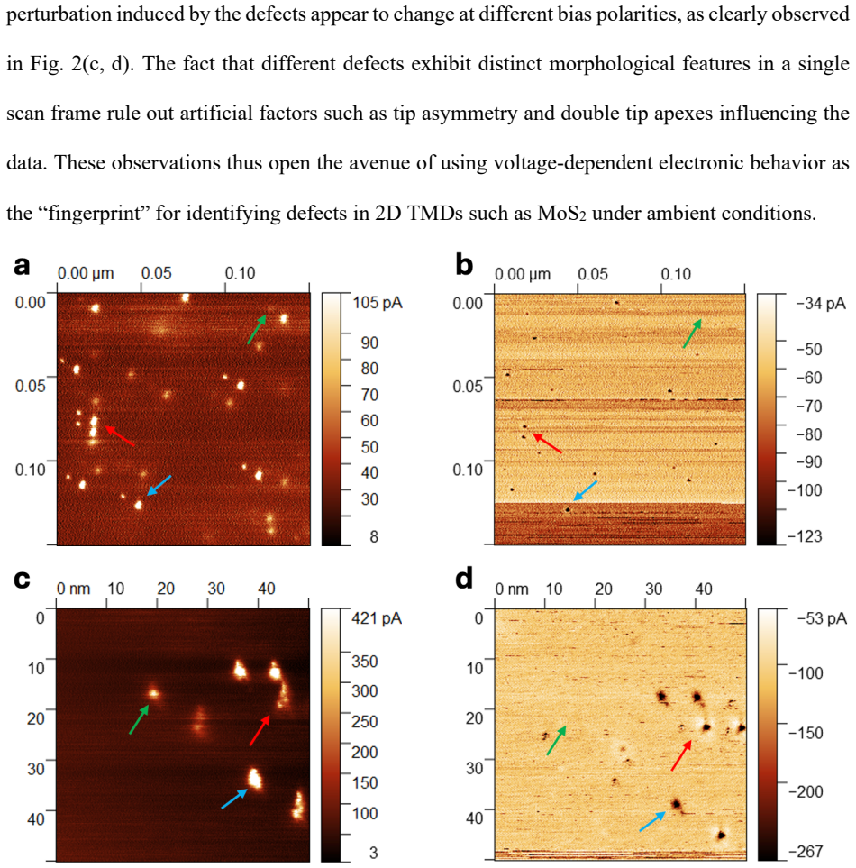
Data acquired in the form of consecutive, high-resolution current maps at various bias voltages allow the assessment of local conductivity and differential conductance as a function of bias voltage for individual defects, the effects of which range from single atomic sites to several nanometers in lateral size. Characteristic behavior in spectroscopy data allows the categorization of observed defects into distinct groups, and their chemical identification as n-type and p-type transition metal substitutions of molybdenum atoms, as well as oxygen substitutions of sulfur atoms.
What carries the argument
Conductive atomic force microscopy (C-AFM) that records bias-dependent current maps to extract local conductivity and differential conductance for each defect site.
If this is right
- Defect influence spans single atomic sites to several nanometers in lateral extent.
- Spectroscopy data permit grouping of defects by their distinct voltage-dependent responses.
- The groups correspond to n-type and p-type transition-metal substitutions on molybdenum sites plus oxygen substitutions on sulfur sites.
- All measurements and identifications occur under ambient air conditions rather than vacuum.
Where Pith is reading between the lines
- The same bias-dependent current mapping could be used on other two-dimensional materials to screen defect populations during device fabrication.
- Knowing the exact substitution type for each defect may help predict how carrier type and density vary across a given MoS2 flake.
- Extending the voltage range or adding temperature control could expose additional defect signatures not captured in the present maps.
Load-bearing premise
The patterns in local conductivity and differential conductance maps are sufficiently unique and unambiguous to assign specific chemical identities to defects without separate chemical analysis or simulations.
What would settle it
A defect whose conductivity-versus-voltage curve fits none of the reported groups or fits more than one group equally well would show that the identification step is not unambiguous.
Figures


read the original abstract
Transition metal dichalcogenides (TMDs) attract significant attention as potential building blocks in next-generation electronic devices. On the other hand, a comprehensive understanding of how various defects affect local electronic properties under realistic operational conditions is yet to be formed. Here, we present results of electronic spectroscopy experiments performed on individual defects in the prototypical TMD molybdenum disulfide (MoS2) under ambient conditions, by way of conductive atomic force microscopy (C-AFM). Data acquired in the form of consecutive, high-resolution current maps at various bias voltages allow the assessment of local conductivity and differential conductance as a function of bias voltage for individual defects, the effects of which range from single atomic sites to several nanometers in lateral size. Characteristic behavior in spectroscopy data allows the categorization of observed defects into distinct groups, and their chemical identification as n-type and p-type transition metal substitutions of molybdenum atoms, as well as oxygen substitutions of sulfur atoms.
Editorial analysis
A structured set of objections, weighed in public.
Referee Report
Summary. The manuscript reports conductive atomic force microscopy (C-AFM) experiments performed on individual atomic defects in MoS2 under ambient conditions. Consecutive high-resolution current maps acquired at varying bias voltages are used to extract local conductivity and differential conductance spectra for defects ranging from single atomic sites to several nanometers in size. Observed characteristic behaviors in these spectra are used to categorize defects into distinct groups and to assign chemical identities as n-type and p-type transition metal substitutions on Mo sites as well as oxygen substitutions on S sites.
Significance. If the chemical assignments hold, the work would demonstrate a practical route to electronic spectroscopy of defects in TMDs without requiring ultra-high vacuum, which is relevant for understanding and mitigating defects in realistic device environments. The approach of mapping voltage-dependent local conductivity at high spatial resolution is a useful experimental contribution. However, the significance is reduced by the absence of independent theoretical predictions or calibrated reference measurements to anchor the assignments.
major comments (2)
- [Results (defect grouping and chemical assignment paragraphs)] The central claim of unambiguous chemical identification (abstract and results section on defect categorization) rests on qualitative pattern recognition in C-AFM conductivity and dI/dV maps. No DFT calculations of expected local density of states or transport signatures for the proposed defect types are presented, nor are reference experiments on intentionally doped or annealed samples used for calibration. This leaves the assignments vulnerable to alternative interpretations such as adsorbate effects or tip-induced band bending under ambient conditions.
- [Methods and Results (spectroscopy data analysis)] No error analysis, statistical measures of group separation, or reproducibility metrics across multiple samples or tips are described for the categorization into n-type, p-type, and oxygen-related groups. Without these, it is difficult to assess whether the observed behaviors constitute unique fingerprints.
minor comments (2)
- [Figures] Figure captions and axis labels for the current maps and extracted spectra should explicitly state the bias voltage range and any normalization procedures applied to the differential conductance data.
- [Discussion] The manuscript would benefit from a brief discussion of how tip-sample contact resistance or ambient humidity might influence the observed local conductivity contrasts.
Simulated Author's Rebuttal
We thank the referee for the constructive and detailed feedback on our manuscript. We address each major comment below and will revise the manuscript accordingly to improve clarity and robustness.
read point-by-point responses
-
Referee: [Results (defect grouping and chemical assignment paragraphs)] The central claim of unambiguous chemical identification (abstract and results section on defect categorization) rests on qualitative pattern recognition in C-AFM conductivity and dI/dV maps. No DFT calculations of expected local density of states or transport signatures for the proposed defect types are presented, nor are reference experiments on intentionally doped or annealed samples used for calibration. This leaves the assignments vulnerable to alternative interpretations such as adsorbate effects or tip-induced band bending under ambient conditions.
Authors: We agree that the assignments are based on observed characteristic spectral features interpreted through the lens of established defect physics in MoS2. While this work does not include new DFT calculations or intentionally doped reference samples, the n-type, p-type, and oxygen-related signatures align with doping effects and substitutional defects reported in prior literature. We acknowledge that ambient conditions can introduce adsorbate or band-bending effects, which we already note as a limitation. In revision we will expand the discussion section with additional literature references to theoretical LDOS predictions and explicitly qualify the assignments as literature-supported interpretations rather than direct chemical proof. revision: partial
-
Referee: [Methods and Results (spectroscopy data analysis)] No error analysis, statistical measures of group separation, or reproducibility metrics across multiple samples or tips are described for the categorization into n-type, p-type, and oxygen-related groups. Without these, it is difficult to assess whether the observed behaviors constitute unique fingerprints.
Authors: We thank the referee for highlighting this point. The original submission emphasized representative spectra to demonstrate the distinct categories. For the revised manuscript we will add quantitative support, including averaged spectra with standard deviations for each group, histograms of key spectral parameters, and data collected across multiple samples and tips to quantify reproducibility and group separation. revision: yes
Circularity Check
No significant circularity; experimental pattern recognition is self-contained.
full rationale
The paper reports C-AFM current maps and differential conductance data on MoS2 defects under ambient conditions. Defects are grouped by observed spatial extent and bias-dependent conductivity contrasts, then assigned chemistries (n-type/p-type metal substitutions on Mo sites, O on S sites) via qualitative pattern matching. No equations, fitted parameters, self-citations of uniqueness theorems, or ansatzes appear in the derivation chain. The central claim rests on direct experimental observations rather than any reduction to prior inputs by construction, making the analysis independent and non-circular.
Axiom & Free-Parameter Ledger
Reference graph
Works this paper leans on
-
[1]
discrete I-V spectroscopy
1 Electronic Spectroscopy of Atomic Defects in Molybdenum Disulfide under Ambient Conditions Joshua R. Evans1, Diego A. Garibay2, Aiden N. Kuhls2, and Mehmet Z. Baykara2,a) 1 Department of Materials Science and Engineering, University of California Merced, Merced, CA 95343, USA 2 Department of Mechanical and Aerospace Engineering, University of California...
2004
-
[2]
Electric Field Effect in Atomically Thin Carbon Films
(a) A 10 × 10 nm2 current map on MoS2 imaged at a bias voltage of -1 V, where two point defects are detected. (b) Average current plotted as a function of the bias voltage for the point defect highlighted by the dashed black circle in (a) (blue), as well as a non-defective (i.e., background) region in its vicinity (orange). The two sets of points are fitt...
work page internal anchor Pith review doi:10.1126/science.1102896 2004
-
[3]
DOI: 10.1038/s41467-025-62370-0. (9) Yang, Y.; Xu, K.; Pena, T.; Neilson, K.; Zheng, X.; Hoang, A.; Yang, K.; Hennighausen, Z.; Zhang, T.; Holtzman, L.; et al. Nondestructive Atomic Defect Quantification of Two-Dimensional Materials and Devices. ACS Applied Materials & Interfaces 2026, 18 (6), 10161-10170. DOI: 10.1021/acsami.5c19328. (10) Liu, S.; Liu, Y...
-
[4]
DOI: 10.1038/s41467-019-11342-2. (12) Sumaiya, S. A.; Liu, J.; Baykara, M. Z. True Atomic-Resolution Surface Imaging and Manipulation under Ambient Conditions via Conductive Atomic Force Microscopy. ACS Nano 2022, 16 (12), 20086-20093. DOI: 10.1021/acsnano.2c08321. 16 (13) Sumaiya, S.; Baykara, M. Atomic-scale imaging and spectroscopy via scanning probe m...
-
[5]
DOI: 10.1186/1556-276X-9-676. (22) Hong, J.; Hu, Z.; Probert, M.; Li, K.; Lv, D.; Yang, X.; Gu, L.; Mao, N.; Feng, Q.; Xie, L.; et al. Exploring atomic defects in molybdenum disulphide monolayers. Nature Communications 2015, 6,
-
[6]
(23) Santosh, K.; Longo, R.; Addou, R.; Wallace, R.; Cho, K
DOI: 10.1038/ncomms7293. (23) Santosh, K.; Longo, R.; Addou, R.; Wallace, R.; Cho, K. Impact of intrinsic atomic defects on the electronic structure of MoS2 monolayers. Nanotechnology 2014, 25 (37), 375703. DOI: 10.1088/0957-4484/25/37/375703. (24) Trainer, D.; Nieminen, J.; Bobba, F.; Wang, B.; Xi, X.; Bansil, A.; Iavarone, M. Visualization of defect ind...
-
[7]
DOI: 10.1038/s41699-022-00286-9
discussion (0)
Sign in with ORCID, Apple, or X to comment. Anyone can read and Pith papers without signing in.