Recognition: unknown
Investigation of the in-pixel response of the Mupix11 monolithic pixel sensor using a microfocus X-ray beam at Diamond Light Source
Pith reviewed 2026-05-07 17:06 UTC · model grok-4.3
The pith
The MuPix11 monolithic pixel sensor displays uniform in-pixel response to an 8 keV X-ray beam at nominal voltage and threshold.
A machine-rendered reading of the paper's core claim, the machinery that carries it, and where it could break.
Core claim
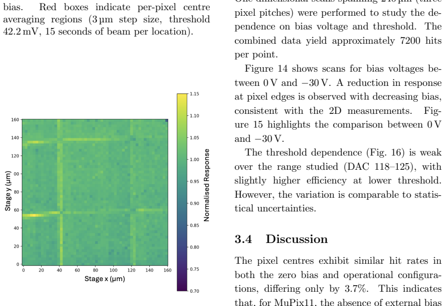
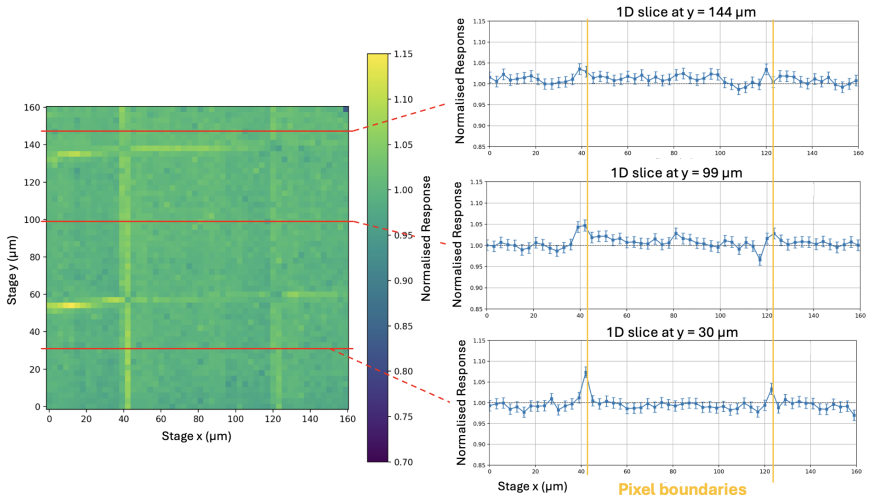
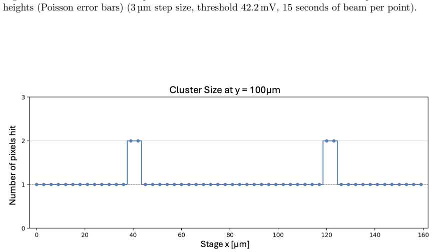
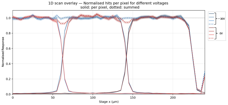
High-resolution scans across the pixel matrix of the 70 micrometer thick MuPix11 sensor reveal uniform detector response at nominal operating voltage and threshold. The relative sub-pixel response becomes location-dependent in the absence of reverse bias, with reduced detection rates observed at pixel boundaries.
What carries the argument
The microfocus X-ray beam with 3 μm spot size used to map the sub-pixel photon response by scanning across the pixel matrix.
If this is right
- The sensor maintains consistent detection efficiency suitable for precise particle tracking without additional corrections.
- Pixel boundaries do not introduce significant efficiency losses under normal bias conditions.
- The thinning to 70 μm preserves the uniform response needed for the Mu3e experiment.
- Zero-bias operation is unsuitable due to position-dependent response variations.
Where Pith is reading between the lines
- If the X-ray emulation of MIPs is accurate, similar sensors could be qualified using this non-destructive method before installation.
- These findings suggest that boundary effects in monolithic sensors can be mitigated by applying reverse bias, which may generalize to other HV-MAPS designs.
- Direct comparison experiments with actual particle beams would further confirm the validity of the X-ray results for real-world use.
Load-bearing premise
The 8 keV X-ray beam with 3 μm spot size accurately emulates the passage of a minimum ionising particle in terms of charge deposition and detection.
What would settle it
A scan at nominal voltage and threshold that shows more than a few percent variation in detection rate between the center and edges of a pixel would contradict the uniformity claim.
Figures


read the original abstract
MuPix11 is a High-Voltage Monolithic Active Pixel Sensor (HV-MAPS) developed for the tracking system of the Mu3e experiment. The in-pixel photon response of a MuPix11 sensor thinned to 70 {\mu}m was measured using an 8 keV X-ray beam with a 3 {\mu}m spot size at the B16 beamline at Diamond Light Source, emulating the passage of a minimum ionising particle (MIP). At nominal operating voltage and threshold, high-resolution scans across the pixel matrix show the detector response to be uniform. In the absence of reverse bias (0 V), the relative sub-pixel response is location-dependent as a reduced detection rate is observed at pixel boundaries.
Editorial analysis
A structured set of objections, weighed in public.
Referee Report
Summary. The manuscript reports experimental measurements of the in-pixel response of the MuPix11 HV-MAPS sensor (thinned to 70 μm) using a 3 μm spot-size 8 keV X-ray beam at the B16 beamline of Diamond Light Source. The central result is that the detector response is uniform across the pixel matrix at nominal operating voltage and threshold, while at 0 V bias the sub-pixel response becomes location-dependent with reduced detection rate at pixel boundaries.
Significance. If the X-ray measurements are representative of MIP interactions, the work supplies high-resolution sub-pixel characterization data directly relevant to the Mu3e tracking system. The controlled microfocus scans provide a useful complement to particle-beam tests by mapping in-pixel variations that are otherwise difficult to resolve.
major comments (1)
- [Abstract] Abstract: The assertion that the 8 keV X-ray beam 'emulates the passage of a minimum ionising particle (MIP)' is not supported by any quantitative comparison (e.g., sub-pixel hit-efficiency maps, collected-charge distributions, or boundary-effect metrics) between the X-ray data and MIP test-beam data. Because 8 keV photoelectric absorption produces a compact charge cloud whose depth and lateral diffusion differ from the extended ionization trail of a MIP (including delta rays), the observed uniformity at nominal bias could be specific to the X-ray interaction and may not hold for MIP tracking in the thinned sensor.
minor comments (2)
- The manuscript lacks explicit quantitative metrics (standard deviation, uniformity maps, or statistical tests) used to establish 'uniform' response and does not report error analysis or uncertainties on the detection-rate measurements.
- Methods details on beam energy calibration, sensor bias and threshold settings, and the precise definition of 'nominal operating voltage and threshold' should be expanded for reproducibility.
Simulated Author's Rebuttal
We thank the referee for the positive evaluation of the work's significance and for the detailed comment on the abstract. We address the concern below and will revise the manuscript accordingly.
read point-by-point responses
-
Referee: [Abstract] Abstract: The assertion that the 8 keV X-ray beam 'emulates the passage of a minimum ionising particle (MIP)' is not supported by any quantitative comparison (e.g., sub-pixel hit-efficiency maps, collected-charge distributions, or boundary-effect metrics) between the X-ray data and MIP test-beam data. Because 8 keV photoelectric absorption produces a compact charge cloud whose depth and lateral diffusion differ from the extended ionization trail of a MIP (including delta rays), the observed uniformity at nominal bias could be specific to the X-ray interaction and may not hold for MIP tracking in the thinned sensor.
Authors: We agree that the manuscript does not include a direct quantitative comparison (such as hit-efficiency maps or charge distributions) between the X-ray results and MIP test-beam data. This paper is dedicated to high-resolution sub-pixel mapping with the microfocus X-ray beam, which provides spatial resolution difficult to achieve with particle beams. We will revise the abstract to remove the claim that the beam 'emulates' MIP passage and instead state that the measurements supply detailed in-pixel response data relevant to the Mu3e tracking system. We will also add a short clarifying paragraph in the introduction noting the complementary character of these X-ray scans to existing MIP tests, without asserting equivalence of the charge-deposition processes. revision: yes
Circularity Check
No circularity: pure experimental measurement of sensor response
full rationale
The paper consists of direct experimental scans of a thinned HV-MAPS sensor using a microfocus 8 keV X-ray beam. Central claims (uniformity at nominal bias/threshold, location dependence at 0 V) are reported observations from data, with no equations, fitted models, predictions, or derivations that reduce to inputs. The phrase 'emulating the passage of a MIP' is an interpretive statement about the measurement technique, not a load-bearing derivation or self-referential fit. No self-citations appear in the provided abstract or description that justify uniqueness or ansatz choices. This is a standard experimental report whose results stand or fall on the data collection itself.
Axiom & Free-Parameter Ledger
axioms (1)
- domain assumption An 8 keV X-ray microbeam produces charge deposition profiles sufficiently similar to those of minimum-ionising particles for response mapping purposes.
Reference graph
Works this paper leans on
-
[1]
MuPix: an HV-MAPS for the Mu3e experiment
Heiko Augustin, Niklaus Berger, Sebastian Dittmeier, Florian Frauen, David Max- imilian Immig, Dohun Kim, Richard Leys, Lukas Mandok, Annie Meneses Gonzalez, Marius Menzel, Ivan Peri´ c, Andr´ e Sch¨ oning, Jackob Stricker, Luigi Vigani, Alena Weber, and Benjamin Weinl¨ ader. MuPix: an HV-MAPS for the Mu3e experiment. InProceedings of the 31st Internation...
-
[2]
D Berst, B Casadei, G Claus, C Colledani, W Dulinski, Y Hu, D Husson, J
R Turchetta, J. D Berst, B Casadei, G Claus, C Colledani, W Dulinski, Y Hu, D Husson, J. P Le Normand, J. L Riester, G Deptuch, U Goerlach, S Higueret, and M Winter. A monolithic active pixel sensor for charged particle tracking and imaging using standard VLSI CMOS technology. Nuclear Instruments and Methods in Physics Research Section A: Accelerators, Sp...
-
[3]
doi: 10.1016/ S0168-9002(00)00893-7
ISSN 0168-9002. doi: 10.1016/ S0168-9002(00)00893-7. URLhttps: //www.sciencedirect.com/science/ article/pii/S0168900200008937
-
[4]
Arndt, H
K. Arndt, H. Augustin, P. Baesso, N. Berger, et al. Technical design of the phase I Mu3e experiment.Nuclear Instru- ments and Methods in Physics Research Section A: Accelerators, Spectrometers, Detectors and Associated Equipment, 1014:165679, October 2021. ISSN 0168-
2021
-
[5]
URLhttps://linkinghub.elsevier
doi: 10.1016/j.nima.2021.165679. URLhttps://linkinghub.elsevier. com/retrieve/pii/S0168900221006641
-
[6]
K. J. S. Sawhney, I. P. Dolbnya, M. K. Tiwari, L. Alianelli, S. M. Scott, G. M. Preece, U. K. Pedersen, and R. D. Wal- ton. A Test Beamline on Diamond Light Source.AIP Conference Proceedings, 1234 (1):387–390, June 2010. ISSN 0094-243X. doi: 10.1063/1.3463220. URLhttps:// doi.org/10.1063/1.3463220
-
[7]
PhD thesis, University of Heidelberg, Heidelberg, 2026
David Maximilian Immig.Straggling in Underdepleted Ultra-Thin Silicon HV- CMOS Sensors. PhD thesis, University of Heidelberg, Heidelberg, 2026. URL https://archiv.ub.uni-heidelberg. de/volltextserver/38033/
2026
-
[8]
S.M. Sze and Kwok K. Ng.Physics of Semiconductor Devices. Wiley, 1 edition, October 2006. ISBN 978-0-471- 14323-9. doi: 10.1002/0470068329. URL https://onlinelibrary.wiley.com/ doi/book/10.1002/0470068329
-
[9]
Ivan Peri´ c, Mridula Prathapan, Heiko Au- gustin, Mathieu Benoit, Raimon Casanova Mohr, Dominik Dannheim, Felix Ehrler, Fadoua Guezzi Messaoud, Moritz Kiehn, Andreas N¨ urnberg, Rudolf Schimassek, Mateus Vicente Barreto, Eva Vilella Figueras, Alena Weber, Winnie Wong, and Hui Zhang. A high-voltage pixel sensor for the ATLAS upgrade.Nuclear Instru- ments ...
-
[10]
H. Augustin, R. Diener, S. Dittmeier, P. M. Freeman, J. Hammerich, A. Herkert, L. Huth, D. Immig, U. Kr¨ amer, N. Meyn- ers, I. Peri´ c, O. Sch¨ afer, A. Sch¨ oning, A. Simancas, M. Stanitzki, D. Stu- art, and B. Weinl¨ ader. Upgrading the beam telescopes at the DESY II Test Beam Facility.Nuclear Instruments and Methods in Physics Research Section A: Acce...
-
[11]
Interferometric signatures of black holes with multiple photon spheres.Phys
S. Navas, C. Amsler, T. Gutsche, et al. Review of Particle Physics.Physical Re- view D, 110(3):030001, August 2024. ISSN 2470-0010. doi: 10.1103/PhysRevD.110. 030001. URLhttps://link.aps.org/ doi/10.1103/PhysRevD.110.030001
-
[12]
W. Riegler and G. Aglieri Rinella. Time resolution of silicon pixel sensors.Jour- nal of Instrumentation, 12(11):P11017, 12 November 2017. ISSN 1748-0221. doi: 10.1088/1748-0221/12/11/P11017. URL https://iopscience.iop.org/article/ 10.1088/1748-0221/12/11/P11017
-
[13]
Springer Berlin Heidelberg, May 2007
Gerhard Lutz.Semiconductor Radiation Detectors: Device Physics. Springer Berlin Heidelberg, May 2007. ISBN 978-3-540- 71678-5
2007
-
[14]
Tables of X-Ray Mass Attenuation Coefficients and Mass Energy-Absorption Coefficients, NIST Standard Reference Database 126, 1995
Stephen Seltzer. Tables of X-Ray Mass Attenuation Coefficients and Mass Energy-Absorption Coefficients, NIST Standard Reference Database 126, 1995. URLhttp://www.nist.gov/pml/data/ xraycoef/index.cfm
1995
-
[15]
Data Flow in the Mu3e DAQ.IEEE Transactions on Nuclear Science, 70(6):898–905, June 2023
Marius K¨ oppel. Data Flow in the Mu3e DAQ.IEEE Transactions on Nuclear Science, 70(6):898–905, June 2023. ISSN 1558-1578. doi: 10.1109/TNS.2023.3276470. URL https://ieeexplore.ieee.org/ abstract/document/10126097
-
[16]
Charakterisierung eines HV-MAPS f¨ ur das P2-Experiment,
Moritz Amadeus Lill. Charakterisierung eines HV-MAPS f¨ ur das P2-Experiment,
-
[17]
URLhttps://www.psi.ch/en/ media/107668/download?attachment. 13
discussion (0)
Sign in with ORCID, Apple, or X to comment. Anyone can read and Pith papers without signing in.