Beyond lead halide perovskites: visible light photovoltaics with phase engineered bismuth-based oxide double-perovskites, Bi2MCrO6 (M = Fe, Mn)
Pith reviewed 2026-05-07 15:58 UTC · model grok-4.3
The pith
Bismuth-based oxide double-perovskites Bi2MCrO6 form the active layer in the first reported visible-light solar cells of this class, reaching 3.56% efficiency.
A machine-rendered reading of the paper's core claim, the machinery that carries it, and where it could break.
Core claim
Solution-deposited 350-450 nm films of Bi2MCrO6 (M = Fe, Mn) crystallize in the monoclinic P21/c double-perovskite structure and exhibit optical absorption coefficients of 10^4-10^5 cm^{-1} across the visible range together with carrier densities of 10^{17-20} cm^{-3}. Ultraviolet photoelectron spectroscopy fixes the valence-band maximum and conduction-band minimum, allowing selection of SnO2 and Spiro-OMeTAD contacts. The resulting BMCO solar cell reaches 3.56% efficiency, and drift-diffusion simulations indicate that control of the observed deep-level defects can increase this value significantly.
What carries the argument
The monoclinic P21/c double-perovskite phase in solution-processed Bi2MCrO6 thin films, which supplies the measured visible absorption, band alignment, and initial photovoltaic response.
If this is right
- The high visible absorption coefficient permits effective light harvesting in sub-micron films.
- Determined band-edge positions are compatible with established electron- and hole-transport layers.
- Numerical modeling predicts substantial efficiency gains once deep-level defects are reduced.
- These oxide double-perovskites provide a chemically stable, lead-free platform for thin-film photovoltaics.
Where Pith is reading between the lines
- If defect densities can be lowered without introducing new recombination paths, these materials could reach efficiencies competitive with established thin-film technologies while retaining ambient stability.
- The mixed-valence states observed in the films suggest that compositional tuning of Fe/Mn/Cr ratios may further adjust band gaps or carrier type.
- The same solution-processing route used here could be applied to related bismuth-based double perovskites to explore a wider range of band alignments and absorption edges.
Load-bearing premise
The measured absorption, carrier density, and device efficiency arise primarily from the intended double-perovskite phase rather than from secondary phases or the mixed cation valences already present in the films.
What would settle it
Fabrication and characterization of a BMCO film in which defect density is lowered while phase purity is verified, followed by a device whose efficiency remains at or below 3.56%.
Figures


read the original abstract
Lead poisoning and notorious ambient instability in lead-based halide perovskites pave the way for the exploration of alternative materials for affordable and efficient solar cell fabrication. An important prerequisite to this end is the optoelectronic evaluation of the proposed material. Here we report, optoelectronic characterization of Bi2FeCrO6 (BFCO) and Bi2MnCrO6 (BMCO) thin films vis-\`a-vis performance of photovoltaic cells. Solution-deposited thin films (350-450 nm) of the above compositions demonstrate a double-perovskite structure with monoclinic P21/c symmetry, albeit with mixed cation valences and deep-level defects. A thorough optoelectronic evaluation exhibits large optical absorption in the visible range ({\alpha} ~ 104 -105 cm-1), and high carrier density, ~1017-20 cm-3. Ultraviolet photoelectron spectroscopy measurement allowed determination of the positions of the band-edges (valence band maximum and conduction band minimum), required for the selection of carrier transport layers. In its first, BMCO-based FTO/SnO2/BMCO/Spiro-OMeTAD/Ag solar cell produced a maximum 3.56% conversion efficiency. Using numerical simulation, we predict that with suitable defect control, the above conversion efficiency can increase significantly.
Editorial analysis
A structured set of objections, weighed in public.
Referee Report
Summary. The manuscript reports synthesis and characterization of Bi2FeCrO6 (BFCO) and Bi2MnCrO6 (BMCO) double-perovskite thin films (350-450 nm) with monoclinic P21/c structure, mixed cation valences, and deep-level defects. It details optoelectronic properties including high visible-range absorption (α ~ 10^4-10^5 cm^{-1}) and carrier densities (~10^{17}-10^{20} cm^{-3}), band-edge positions from UPS, a prototype FTO/SnO2/BMCO/Spiro-OMeTAD/Ag solar cell achieving 3.56% PCE, and numerical simulations predicting substantial efficiency gains via defect control.
Significance. If the experimental device result proves reproducible and the simulation predictions can be made independent of the input data, the work would add modestly to the search for lead-free oxide alternatives to halide perovskites by supplying concrete thin-film absorption, carrier, and band-alignment data plus an initial working cell. The experimental absorption and UPS measurements are useful for transport-layer selection; however, the 3.56% PCE is low relative to established lead-halide devices and the simulation-based improvement claim is the central forward-looking element.
major comments (3)
- [Abstract] Abstract: The headline experimental claim of a maximum 3.56% conversion efficiency in the first BMCO device is presented without error bars, the number of devices tested, full J-V parameters (Voc, Jsc, FF), or baseline comparisons, which are required to evaluate reproducibility and performance.
- [Numerical simulation] Numerical simulation (abstract and results): The prediction that efficiency can increase significantly with defect control uses transport and defect-density parameters calibrated directly to the same thin-film carrier-density (10^{17}-10^{20} cm^{-3}) and deep-level defect data reported in the manuscript, rendering the gain non-independent of the experimental inputs.
- [Optoelectronic characterization] Optoelectronic characterization: The films already exhibit high carrier densities and deep-level defects together with mixed cation valences; the assumption that these densities can be lowered substantially while holding absorption coefficient, band edges, and mobility fixed, without introducing new interface states or phase impurities, lacks experimental support or a proposed synthesis route.
minor comments (2)
- [Abstract] Abstract: Minor formatting and phrasing issues (e.g., 'vis-`a-vis', Greek-letter rendering) should be standardized for journal style.
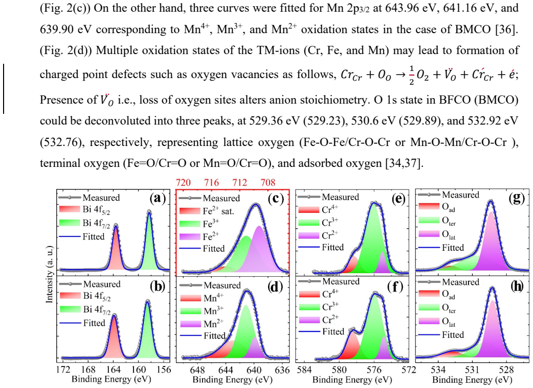
- [Throughout] Throughout: Provide explicit discussion of how the 350-450 nm thickness range affects measured carrier densities and absorption, and ensure all units and symbols are defined on first use.
Simulated Author's Rebuttal
We thank the referee for the constructive and detailed comments on our manuscript. We have addressed each major point below with revisions to improve clarity, completeness, and transparency regarding device statistics, simulation assumptions, and defect control strategies.
read point-by-point responses
-
Referee: [Abstract] Abstract: The headline experimental claim of a maximum 3.56% conversion efficiency in the first BMCO device is presented without error bars, the number of devices tested, full J-V parameters (Voc, Jsc, FF), or baseline comparisons, which are required to evaluate reproducibility and performance.
Authors: We agree that the abstract and main text require additional details for proper evaluation of reproducibility. In the revised manuscript, we have updated the abstract to report the full J-V parameters (Voc, Jsc, FF) for the champion device, the number of devices fabricated and tested (with average PCE and standard deviation), and error bars on the reported efficiency. Baseline comparisons to control devices (e.g., without the BMCO layer) have been added to the results section and supplementary information to contextualize the performance. revision: yes
-
Referee: [Numerical simulation] Numerical simulation (abstract and results): The prediction that efficiency can increase significantly with defect control uses transport and defect-density parameters calibrated directly to the same thin-film carrier-density (10^{17}-10^{20} cm^{-3}) and deep-level defect data reported in the manuscript, rendering the gain non-independent of the experimental inputs.
Authors: The referee is correct that the simulation parameters are derived from our measured carrier densities and defect data. The simulation is intended as a parametric sensitivity analysis to illustrate the potential impact of defect reduction on efficiency, using the experimental values as the baseline. We have revised the abstract and results to explicitly clarify this scope, stating that the projections are not independent predictions but rather demonstrate the performance headroom if defect densities can be lowered while other properties remain comparable. revision: partial
-
Referee: [Optoelectronic characterization] Optoelectronic characterization: The films already exhibit high carrier densities and deep-level defects together with mixed cation valences; the assumption that these densities can be lowered substantially while holding absorption coefficient, band edges, and mobility fixed, without introducing new interface states or phase impurities, lacks experimental support or a proposed synthesis route.
Authors: This is a fair observation, as our current solution-processed films do show high carrier densities and mixed valences. We have added a dedicated discussion paragraph outlining potential mitigation strategies, including post-deposition annealing under reducing atmospheres to passivate defects, aliovalent doping to compensate carriers, and exploration of alternative precursors or deposition techniques. We explicitly note that these approaches lack experimental validation in the present work and that maintaining all other optoelectronic properties unchanged would require further study; this is framed as an important direction for future optimization rather than an established assumption. revision: yes
Circularity Check
Numerical prediction of significantly higher efficiency is obtained by reparameterizing defect densities fitted to the same thin-film measurements
specific steps
-
fitted input called prediction
[Abstract (and simulation section)]
"In its first, BMCO-based FTO/SnO2/BMCO/Spiro-OMeTAD/Ag solar cell produced a maximum 3.56% conversion efficiency. Using numerical simulation, we predict that with suitable defect control, the above conversion efficiency can increase significantly."
The simulation inputs (defect densities, carrier concentrations, band positions) are calibrated to the measured properties of the identical thin films already shown to have high carrier density and deep-level defects. Lowering those densities to forecast higher PCE is therefore a reparameterization of the experimental inputs rather than an independent forward prediction.
full rationale
The paper's central experimental result (3.56% PCE in the first BMCO device) stands on its own. However, the stronger claim that efficiency 'can increase significantly' with defect control reduces to a numerical simulation whose carrier densities, defect levels, absorption coefficients, and band edges are taken directly from the reported optoelectronic characterization of the same films (high carrier density ~10^17-10^20 cm^{-3} and deep-level defects). Adjusting those fitted inputs while holding other quantities fixed produces the 'prediction' by construction. No self-citation chains, uniqueness theorems, or ansatz smuggling are present in the provided text; the circularity is limited to this one fitted-input-called-prediction step.
Axiom & Free-Parameter Ledger
free parameters (1)
- defect density parameters in simulation
axioms (1)
- domain assumption The deposited films adopt the monoclinic P21/c double-perovskite structure with the reported mixed cation valences
Reference graph
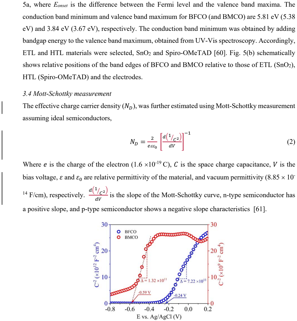
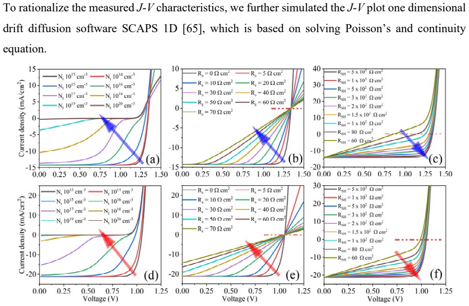
Works this paper leans on
-
[1]
W.-J. Yin, B. Weng, J. Ge, Q. Sun, Z. Li, Y. Yan, Oxide per ovskites, double perovskites and derivatives for electrocatalysi s, photocatalysis, and photovolt aics, Energy Environ. Sci. 12 (2019) 442–462. https://doi.org/10.1039/C8EE01574K
-
[2]
S. Walia, S. Balendhran, H. Nili, S. Zhuiykov, G. Rosengart en, Q.H. Wang, M. Bhaskaran, S. Sriram, M.S. Strano, K. Kalantar-zadeh, Transition metal oxi des – Thermoelectric properties, Progress in Mater ials Science 58 (2013) 1443–1489. https://doi.org/10.1016/j.pmatsci.2013.06.003
-
[3]
M.G. Basavarajappa, S. Cha kraborty, Rationalization of Double Perovskite Oxides as Energy Materials: A Theoretical Insight from Electronic and Optical Pr operties, ACS Materials Au 2 (2022) 655–664. https://doi.org/10.1021/acsmaterialsau.2c00031
-
[4]
S.R. Basu, L.W. Martin, Y.H. Chu, M. Gajek, R. Ramesh, R.C. Rai, X. Xu, J.L. Musfeldt, Photoconductivity in BiFeO3 thin films, Applied Physics Letters 92 (2008) 091905. https://doi.org/10.1063/1.2887908
-
[5]
S. Rahmany, L. Etgar, Semitransparent Perovskite Solar Cell s, ACS Energy Letters 5 (2020) 1519–1531. https://doi.org/10.1021/acsenergylett.0c00417
-
[6]
A.K. Astakala, S.-Y. Lee, J. Gautam, K.B. Thapa, I. In, S.J . Lee, S.-J. Park, Engineering inorganic perovskite solar cells: overcoming efficiency and sta bility barriers for next- generation photovoltaics, Advanced Powder Materials 5 (2026) 10 0354. https://doi.org/doi.org/10.1016/j.apmate.2025.100354
-
[7]
M. Caputo, N. Cefarin, A. Radivo, N. Demitri, L. Gigli, J.R . Plaisier, M. Panighel, G. Di Santo, S. Moretti, A. Giglia, M. P o l e n t a r u t t i , F . D e A n g e l i s , E. Mosconi, P. Umari, M. Tormen, A. Goldoni, Electronic st ructure of MAPbI3 and MAPbCl3: importance of band alignment, Scientific Reports 9 (2019) 15159. https://doi.org/10.1038/s415...
-
[8]
R.E. Brandt, V. Stevanović, D.S. Ginley, T. Buonassisi, Ide ntifying defect-tolerant semiconductors with high minority-carrier lifetimes: Beyond hybrid lead halide perovskites, MRS Communications 5 (2015) 265–275. https://doi.org/10.1557/mrc.2015.26
-
[9]
S. Sradhasagar, O. Subhasish Khuntia, S. Biswal, S. Purohit , A. Roy, Machine learning-aided discovery of bismuth-based tran sition metal oxide double perovs kites for solar cell applications, Solar Energy 267 (2024) 112209. https://doi.org/10.1016/j.solener.2023.112209. 21
-
[10]
R. Nechache, C. Harnagea, L.-P. Carignan, D. Ménard, A. Pi gnolet, Epitaxial Bi2FeCrO6 multiferroic thin films, Philosophical Magazine Letters 87 (200 7) 231–240. https://doi.org/10.1080/09500830601153402
-
[11]
R. Nechache, C. Harnagea, L.-P. Carignan, O. Gautreau, L. Pintilie, M.P. Singh, D. Ménard, P. Fournier, M. Alexe, A. Pignolet, Epitaxial thin films of the multiferroic double perovskite Bi2FeCrO6 grown on (100)-oriente d SrTiO3 substrates: Growth, ch aracterization, and optimization, Journal of App lied Physics 105 (2009) 061621. https://doi.org/10.1063/1.3073826
-
[12]
R. Nechache, C. Harnagea, S. Licoccia, E. Traversa, A. Rue diger, A. Pignolet, F. Rosei, Photovoltaic properties of Bi2FeCrO6 epitaxial thin films, Applied Physics Letters 98 (2011) 202902. https://doi.org/10.1063/1.3590270
-
[13]
N.A. Mahammedi, A. Benameur, H. Gueffaf, B. Merabet, O.M. Ozkendir, S.-I. Sato, Investigating a Pb-free n-i-p perovskite solar cell with BFCO a bsorber using SCAPS-1D, Optik 302 (2024) 171659. https://doi.org/10.1016/j.ijleo.2024.171659
-
[14]
W. Huang, C. Harnagea, X. Tong, D. Benetti, S. Sun, M. Cha ker, F. Rosei, R. Nechache, Epitaxial Bi2FeCrO6 Multiferroic Thin-Film Photoanodes with Ultrathin p-Type NiO Layers for Improved Solar Water Oxidation, ACS Applied Materials & Interfaces 11 (2019) 13185– 13193. https://doi.org/10.1021/acsami.8b20998
-
[15]
S. Li, B. AlOtaibi, W. Huang, Z. Mi, N. Serpone, R. Nechac he, F. Rosei, Epitaxial Bi2FeCrO6 Multiferroic Thin Film as a New Visible Light Absorbi ng Photocathode Material, Small 11 (2015) 4018–4026. https://doi.org/doi.org/10.1002/smll.201403206
-
[16]
L. Wei, J. Guo, L. Guan, B. Liu, First-principles investig ation of bandgap tailoring in tetragonal Bi2FeCrO6 by magnetic ordering and B-site-cation ordering, Functional Materials Letters 13 (2019) 1950092. https://doi.org/10.1142/S1793604719500929
-
[17]
R. Nechache, C. Harnagea, S. Li, L. Cardenas, W. Huang, J. Chakrabartty, F. Rosei, Bandgap tuning of multiferroic oxide solar cells, Nature Photonics 9 (2 014) 61–67. https://doi.org/10.1038/nphoton.2014.255
-
[18]
W. Huang, J. Chakrabartty, C. Harnagea, D. Gedamu, I. Ka, M . C h a k e r , F . R o s e i , R . Nechache, Highly Sensitive Switchable Heterojunction Photodiode Based on Epitaxial Bi2FeCrO6 Multiferroic Thin Films, ACS Applied Materials & Interfaces 10 (2018) 12790– 12797. https://doi.org/10.1021/acsami.8b00459. 22
-
[19]
B. Merabet, H. Alamri, M. Djermouni, A. Zaoui, S. Kacimi, A. Boukortt, M. Bejar, Optimal Bandgap of Double Perovskite La-Substituted Bi2FeCrO6 for Solar Cells: an ab initio GGA+U Study, Chinese Physics Le tters 34 (2017) 016101. https:// doi.org/10.1088/0256- 307X/34/1/016101
-
[20]
A. Raj, M. Kumar, A. Kumar, K. Singh, S. Sharma, R.C. Singh, M.S. Pawar, M.Z.A. Yahya, A. Anshul, Comparative analysis of ‘La’ modified BiFeO3-based p erovskite solar cell devices for high conversion effi ciency, Ceramics International 49 (2023) 1317–1327. https://doi.org/https://doi.org/10.1016/j.ceramint.2022.09.112
-
[21]
C. Senthilkumar, F.W. Shash ikanth, Room temperature weak f erromagnetism in new Bi2MnCrO6 synthesized by gel co mbustion method, Applied Physics A 128 (2022) 244. https://doi.org/10.1007/s00339-022-05400-8
-
[22]
G. Kumar, B.K. Ravidas, S. Bhattarai, M.K. Roy, D.P. Samaj dar, Exploration of the photovoltaic properties of oxide-based double perovskite Bi2FeCrO6 using an amalgamation of DFT with spin–orbit coupling effect and SCAPS-1D simulation approaches, New J. Chem. 47 (2023) 18640–18658. https://doi.org/10.1039/D3NJ02841K
-
[23]
S.K. Gupta, A. Kumar, S. Barthwal, Sadanand, N. Garg, C.K. Gupta, V. Yadav, S. Sharma, D.C. Tripathi, S. Kumar, SCAPS-1D study on the design and perfo rmance optimization of Sr3NCl3 solar cell: Assessing the significance of copper oxide (Cu2O) and copper(I) thiocyanate (CuSCN) as hole tran sport layers, Journal of Physic s and Chemistry of Solids 208 (202...
-
[24]
L.A. Lotfy, M. Abdelfatah, S.W. Sharshir, A.A. El-Naggar, W . I s m a i l , A . E l - S h a e r , Numerical simulation and optimiza tion of FTO/TiO2/CZTS/CuO/Au s olar cell using SCAPS-1D, Scientific Reports 15 (2025) 28022. https://doi.org/10.1038/s41598-025-12999- 0
-
[25]
A. Saidarsan, S. Guruprasad, A. Malik, P. Basumatary, D.S. Ghosh, A critical review of unrealistic results in SCAPS-1D simulations: Causes, practical solutions and roadmap ahead, Solar Energy Materials and Solar Cells 279 (2025) 113230. https://doi.org/10.1016/j.solmat.2024.113230
-
[26]
N. Bhardwaj, A. Gaur, K. Yadav, Effect of doping on optical properties in BiMn1−x(TE)xO3 (where x = 0.0, 0.1 and TE = Cr, Fe, Co, Zn) nanoparticles synt hesized by microwave and 23 sol-gel methods, Applied Physics A 123 (2017) 429. https://doi. org/10.1007/s00339-017- 1042-y
-
[27]
F. Bai, L. Shi, H. Zhang, Z. Zhong, W. Wang, D. He, Multif erroic properties of La-doped Bi2FeCrO6 prepared by high-pre ssure synthesis, Journal of Appli ed Physics 111 (2012) 07C702. https://doi.org/10.1063/1.3670576
-
[28]
W. Xu, J. Sun, X. Xu, G. Yuan, Y. Zhang, J. Liu, Z. Liu, Reproducible resistive switching in the super-thin Bi2FeCrO6 epitaxial film with SrRuO3 bottom elec trode, Applied Physics Letters 109 (2016) 152903. https://doi.org/10.1063/1.4964603
-
[29]
P. Mandal, A. Iyo, Y. Tanaka, A. Sundaresan, C.N.R. Rao, S tructure, magnetism and giant dielectric constant of BiCr0.5Mn0.5O3 synthesized at high press ures, Journal of Materials Chemistry 20 (2010) 1646–1650. https://doi.org/10.1039/B914350P
-
[30]
A. Quattropani, D. Stoeffler, T. Fix, G. Schmerber, M. Lenertz, G. Versini, J.L. Rehspringer, A. Slaoui, A. Dinia, S. Colis, Band-Gap Tuning in Ferroelectric Bi2FeCrO6 Double Perovskite Thin Films, The Journal of Physical Chemistry C 122 (2018) 1070–1077. https://doi.org/10.1021/acs.jpcc.7b10622
-
[31]
R. Nechache, C. Harnagea, A. Pignolet, F. Normandin, T. Veres, L.-P. Carignan, D. Ménard, Growth, structure, and propertie s of epitaxial thin films of fi rst-principles predicted multiferroic Bi2FeCrO6, Applie d Physics Letters 89 (2006) 10290 2. https://doi.org/10.1063/1.2346258
-
[32]
L. Qiao, K.H.L. Zhang, M.E. Bowden, T. Varga, V. Shutthana ndan, R. Colby, Y. Du, B. Kabius, P.V. Sushko, M.D. Biegalski, S.A. Chambers, The Impacts of Cation Stoichiometry and Substrate Surface Quality on Nucleation, Structure, Defect Formation, and Intermixing in Complex Oxide Heteroepitaxy–LaCrO3 on SrTiO3(001), Advanced Functional Materials 23 (2013) ...
-
[33]
S. Yuan, Z. Mu, L. Lou, S. Zhao, D. Zhu, F. Wu, Broadband NIR-II phosphors with Cr4+ single activated centers based on special crystal structure for nondestructive analysis, Ceramics International 48 (2022) 26884–26893. https://doi.org/10.1016/j.ceramint.2022.05.391
-
[34]
H. Wu, Z. Pei, W. Xia, Y. Lu, K. Leng, X. Zhu, Structural, magnetic, dielectric and optical properties of double-perovskite B i2FeCrO6 ceramics synthesized under high pressure, 24 Journal of Alloys and Compounds 819 (2020) 153007. https://doi.org/doi.org/10.1016/j.jallcom.2019.153007
-
[35]
G.A. Gomez-Iriarte, A. Pent ón-Madrigal, L.A.S. De Oliveira, J.P. Sinnecker, XPS Study in BiFeO3 Surface Modified by Ar gon Etching, Materials 15 (2022) 4 285. https://doi.org/10.3390/ma15124285
-
[36]
J.-W. Shi, C. Gao, C. Liu, Z. Fan, G. Gao, C. Niu, Porous MnOx for low-temperature NH3- SCR of NOx: the intrinsic rela tionship between surface physicoc hemical property and catalytic activity, Journal of N anoparticle Research 19 (2017) 194. https://doi.org/10.1007/s11051-017-3887-6
-
[37]
C. Chen, X.-T. Wang, J.- H. Zhong, J. Liu, G.I.N. Waterhouse, Z.-Q. Liu, Epitaxially Grown Heterostructured SrMn3O6−x-SrMnO3 with High-Valence Mn3+/4+ for Improved Oxygen Reduction Catalysis, Angewandte Chemie International Edition 60 (2021) 22043–22050. https://doi.org/doi.org/10.1002/anie.202109207
-
[38]
M.T. Anderson, K.B. Greenwood, G.A. Taylor, K.R. Poeppelme ier, B-cation arrangements in double perovskites, Progress in Solid State Chemistry 22 (19 93) 197–233. https://doi.org/10.1016/0079-6786(93)90004-B
-
[39]
Y. Li, H. Wu, W. Qi, X. Zhou, J. Li, J. Cheng, Y. Zhao, Y. Li, X. Zhang, Passivation of defects in perovskite solar cell: From a chemistry point of vie w, Nano Energy 77 (2020) 105237. https://doi.org/10.1016/j.nanoen.2020.105237
-
[40]
D.-Y. Son, S.-G. Kim, J.-Y. Seo, S.-H. Lee, H. Shin, D. Lee, N.-G. Park, Universal Approach toward Hysteresis-Free Perovskite Solar Cell via Defect Engineering, J. Am. Chem. Soc. 140 (2018) 1358–1364. https://doi.org/10.1021/jacs.7b10430
-
[41]
M. Abdi-Jalebi, M. Pazoki, B. Philippe, M.I. Dar, M. Alsar i, A. Sadhanala, G. Divitini, R. Imani, S. Lilliu, J. Kullgren, H. Rensmo, M. Grätzel, R.H. Friend, Dedoping of Lead Halide Perovskites Incorporating Monov alent Cations, ACS Nano 12 (2018 ) 7301–7311. https://doi.org/10.1021/acsnano.8b03586
-
[42]
G. Ren, W. Han, Z. Li, C. Liu, L. Shen, W. Guo, Alkali met al ions passivation to decrease interface defects of perovskite s olar cells, Solar Energy 193 ( 2019) 220–226. https://doi.org/10.1016/j.solener.2019.09.056
-
[43]
Y. Guo, F. Zhao, J. Tao, J. Jiang, J. Zhang, J. Yang, Z. H u, J. Chu, Efficient and Hole- Transporting-Layer-Free CsPbI2Br Planar Heterojunction Perovski te Solar Cells through 25 Rubidium Passivation, ChemSusChem 12 (2019) 983–989. https://doi.org/10.1002/cssc.201802690
-
[44]
X. Liu, Y. Zhang, L. Shi, Z. Liu, J. Huang, J.S. Yun, Y. Z eng, A. Pu, K. Sun, Z. Hameiri, J.A. Stride, J. Seidel, M.A. Gr een, X. Hao, Exploring Inorganic Binary Alkaline Halide to Passivate Defects in Low-Temperature-Processed Planar-Structure Hybrid Perovskite Solar Cells, Advanced Energy Materials 8 (2018) 1800138. https://doi.org/10.1002/aenm.201800138
-
[45]
N.E. Grant, S.L. Pain, E. Khorani, R. Jefferies, A. Wratte n, S. McNab, D. Walker, Y. Han, R. Beanland, R.S. Bonilla, J.D. Murphy, Activation of Al2O3 surface passivation of silicon: Separating bulk and surface effects, Applied Surface Science 64 5 (2024) 158786. https://doi.org/10.1016/j.apsusc.2023.158786
-
[46]
F.F. Targhi, Y.S. Jalili, F. Kanjouri, MAPbI3 and FAPbI3 p erovskites as solar cells: Case study on structural, electrical a nd optical properties, Results in Physics 10 (2018) 616–627. https://doi.org/10.1016/j.rinp.2018.07.007
-
[47]
Ł. Haryński, A. Olejnik, K. Grochowska, K. Siuzdak, A facile method for Tauc exponent and corresponding electronic transitions determination in semiconductors directly from UV–Vis spectroscopy data, Optical Materials 127 (2022) 112205. https://doi.org/doi.org/10.1016/j.optmat.2022.112205
-
[48]
A. Quattropani, A.S. Makhort, M.V. Rastei, G. Versini, G. Schmerber, S. Barre, A. Dinia, A. Slaoui, J.-L. Rehspringer, T. Fix, S. Colis, B. Kundys, Tuning photovoltaic response in Bi2FeCrO6 films by ferroelectric poling, Nanoscale 10 (2018) 13 761–13766. https://doi.org/10.1039/C8NR03137A
-
[49]
W. Huang, C. Harnagea, D. Benetti, M. Chaker, F. Rosei, R. Nechache, Multiferroic Bi2FeCrO6 based p–i–n heterojunction photovoltaic devices, Journal of Materials Chemistry A 5 (2017) 10355–10364. https://doi.org/10.1039/C7TA01604B
-
[50]
R. Nechache, L.-P. Carignan, L. Gunawan, C. Harnagea, G.A. Botton, D. Ménard, A. Pignolet, Epitaxial thin films of multiferroic Bi2FeCrO6 with B -site cationic order, Journal of Materials Research 22 (2007) 2102–2110. https://doi.org/10.1557/jmr.2007.0273
-
[51]
B. Nath, P.C. Ramamurthy, D. R. Mahapatra, G. Hegde, Effect of cuprous iodide passivation in perovskite solar cells, Journal of Materials Science: Materi als in Electronics 33 (2022) 14457–14467. https://doi.org/10.1007/s10854-022-08368-6. 26
-
[52]
T.D. Subha, R.T. Prabu, S. Parasuraman, A. Kumar, Role of Urbach energy in controlling voltage output of solar cells, Op tical and Quantum Electronics 55 (2023) 794. https://doi.org/10.1007/s11082-023-05067-2
-
[53]
W. Li, K. Zhao, H. Zhou, W. Yu, J. Zhu, Z. Hu, J. Chu, Pre cursor solution temperature dependence of the optical constants, band gap and Urbach tail i n organic–inorganic hybrid halide perovskite films, J. Phys. D: Appl. Phys. 52 (2019) 0451 03. https://doi.org/10.1088/1361-6463/aaec21
-
[54]
F. Urbach, The Long-Wavele ngth Edge of Photographic Sensit ivity and of the Electronic Absorption of Solids, Physical Review 92 (1953) 1324. https://doi.org/10.1103/PhysRev.92.1324
-
[55]
J.D. Dow, D. Redfield, Towa rd a Unified Theory of Urbach’s Rule and Exponential Absorption Edges, Physical Review B 5 (1972) 594–610. https://doi.org/10.1103/PhysRevB.5.594
-
[56]
G.D. Cody, T. Tiedje, B. Abeles, B. Brooks, Y. Goldstein, Disorder and the Optical- Absorption Edge of Hydrogenated Amorphous Silicon, Physical Rev iew Letters 47 (1981) 1480–1483. https://doi.org/10.1103/PhysRevLett.47.1480
-
[57]
E. Arushanov, L. Kulyuk, O. Kulikova, V. Tezlevan, R.F. Ru iz, M. León, Optical study of monocrystalline CuIn 4 S e 6, J. Phys. D: Appl. Phys. 34 (2001) 3480–3484. https://doi.org/10.1088/0022-3727/34/24/309
-
[58]
M. Kumar, S.K. Pundir, D.V. Singh, M. Kumar, Effect on gre en energy conversion and stability with ‘Er’ modification in multiferroic based perovskite solar cell devices, Materials Today Communications 38 (2024) 107841. https://doi.org/10.1016/j.mtcomm.2023.107841
-
[59]
J. Li, H.A. Dewi, H. Wang, J. Zhao, N. Tiwari, N. Yantara, T. Malinauskas, V. Getautis, T.J. Savenije, N. Mathews, S. Mhaisalkar, A. Bruno, Co-Evaporated MAPbI3 with Graded Fermi Levels Enables Highly Performing , Scalable, and Flexible p-i-n Perovskite Solar Cells, Advanced Functional Materials 31 (2021) 2103252. https://doi.org/doi.org/10.1002/adfm.202103252
-
[60]
P. Murugan, T. Hu, X. Hu, Y. Chen, Current Development tow ard Commercialization of Metal-Halide Perovskite Photovolta ics, Advanced Optical Materia ls 9 (2021) 2100390. https://doi.org/doi.org/10.1002/adom.202100390. 27
-
[61]
H.-Y. Tu, X. Qi, Growth of p/n-type BiFeO3 thin films for construction of a bilayer p–n junction for photodegradation of o rganic pollutants, Journal of Ma teria ls Chem istry A 12 (2024) 12752–12761. https://doi.org/10.1039/D4TA01615G
-
[62]
M.T. Neukom, S. Züfle, E. K napp, M. Makha, R. Hany, B. Ruhstaller, Why perovskite solar cells with high efficiency show small IV-curve hysteresis, Solar Energy Materials and Solar Cells 169 (2017) 159–166. https://doi.org/doi.org/10.1016/j.solmat.2017.05.021
-
[63]
J.C. Wang, X.C. Ren, S.Q. Shi, C.W. Leung, P.K.L. Chan, Ch arge accumulation induced S- shape J–V curves in bilayer heterojunction organic solar cells, Organic Electronics 12 (2011) 880–885. https://doi.org/10.1016/j.orgel.2011.02.016
-
[64]
P. Arnou, C.S. Cooper, A.V. Malkov, J.W. Bowers, J.M. Wall s, Solution-processed CuIn(S,Se)2 absorber layers for application in thin film solar cells, Thin Solid Films 582 (2015) 31–34. https://doi.org/doi.org/10.1016/j.tsf.2014.10.080
-
[65]
A. El Badraoui, T. Chargui, A. Elkhou, B. El Mokhtari, R. El Idrissi, L. El Amri, H. Ez- Zahraouy, N. Tahiri, Optimization of lead-free CsSnBr3-based pe rovskite solar cells via SCAPS-1D simulations and machine learning models, Journal of Ph ysics and Chemistry of Solids 210 (2026) 113340. https://doi.org/10.1016/j.jpcs.2025.113340
-
[66]
V.H.D. Araújo, A.F. Nogueira, J.C. Tristão, L.J. dos Santos, Advances in lead-free perovskite solar cell design via SCAPS-1D simulations, RSC Sustainability 3 (2025) 4314–4335. https://doi.org/10.1039/D5SU00526D
discussion (0)
Sign in with ORCID, Apple, or X to comment. Anyone can read and Pith papers without signing in.