Recognition: unknown
From Defects to Devices: Design Guidelines for High-Performance Diamond-Based Solar Cells and Single-Dopant Diodes
Pith reviewed 2026-05-08 16:51 UTC · model grok-4.3
The pith
Defect structures in diamond create intermediate bands and impurity conduction for solar cells and diodes while preserving high mobility and thermal conductivity.
A machine-rendered reading of the paper's core claim, the machinery that carries it, and where it could break.
Core claim
The central claim is that the BVB defect introduces intermediate bands in diamond without degrading its high carrier mobility or thermal conductivity, while PV-doping provides high conductivity at room temperature through impurity-band transport. Using density functional theory with GW corrections, Bethe-Salpeter equation calculations and carrier transport modelling coupled to device electrostatics via a Poisson solver, the authors derive practical design principles: align incident light in the xz-plane to exploit anisotropic absorption, use graded junctions to reduce tunneling, target an absorber thickness of roughly 500 nm, and exploit contact transparency for bifacial operation. For thePV
What carries the argument
The boron-vacancy-boron (BVB) defect as an intermediate-band absorber and the phosphorus-vacancy (PV) defect as an impurity-band conductor, simulated with first-principles electronic structure methods linked to a Poisson electrostatic solver.
If this is right
- Graded junctions in the PIN cell reduce tunneling losses at abrupt interfaces.
- An absorber thickness near 500 nm balances sufficient light absorption against efficient carrier extraction.
- High transparency of the contact layers supports bifacial solar-cell designs.
- PV-doped regions enable single-dopant PN junctions that simplify manufacturing for tunnel diodes and asymmetric devices.
- Temperature-dependent Seebeck anisotropy in PV-doped diamond opens thermal-management uses.
Where Pith is reading between the lines
- If the defects can be placed controllably, the same principles may apply to other wide-bandgap hosts that suffer from doping-induced mobility loss.
- The Seebeck sign-reversal behavior could be tested for new thermoelectric sensor geometries that combine electrical and thermal functions in one material.
- Extending the modeling to include realistic growth kinetics would help predict which defect densities are achievable by current chemical-vapor-deposition methods.
Load-bearing premise
The simulated BVB and PV defect configurations can be created experimentally in high-quality diamond without extra compensating defects or scattering centers that would lower the predicted mobility and conductivity.
What would settle it
Fabricating a BVB-containing diamond layer and measuring optical absorption spectra that show no intermediate-band features or carrier mobility values significantly below the modeled predictions.
Figures


read the original abstract
This work establishes key technological guidelines for designing diamond-based optoelectronic devices, derived from a first-principles investigation of two architectures: a PIN junction with a boron-vacancy-boron (BVB) intermediate-band absorber, and a PN junction based on phosphorus-vacancy (PV) defects. For the PIN solar cell, practical design principles include: i) aligning incident light in the xz-plane to exploit anisotropic absorption; ii) using graded junctions to mitigate tunnelling losses at abrupt interfaces; iii) targeting an absorber thickness of ~500 nm to balance absorption and carrier extraction; and iv) leveraging the high transparency of both contact layers for bifacial device configurations. For the PN diode, the PV-doped diamond operates via impurity-band conduction, making it suitable for degenerate p-type applications such as tunnel diodes or asymmetric junctions, while its temperature-dependent Seebeck anisotropy and sign-reversal offer opportunities for thermal management applications. When paired with phosphorus-doped n-type regions, these defects enable single-dopant junctions that significantly simplify device manufacturing. Using density functional theory with GW corrections, Bethe-Salpeter equation calculations and carrier transport modelling coupled to device electrostatics via a Poisson solver, we show that the BVB defect introduces intermediate bands without degrading diamond's high carrier mobility or thermal conductivity, while PV-doping provides high conductivity at room temperature through impurity-band transport. Overall, both defect-engineered systems preserve diamond's superior transport and thermal properties even after doping, offering viable pathways for high-performance diamond optoelectronics. These guidelines provide a practical foundation for fabricating efficient diamond-based photovoltaic and diode devices.
Editorial analysis
A structured set of objections, weighed in public.
Referee Report
Summary. The manuscript employs density functional theory with GW corrections, Bethe-Salpeter equation calculations, and carrier transport modeling coupled to device electrostatics via a Poisson solver to study boron-vacancy-boron (BVB) defects as intermediate-band absorbers in PIN diamond solar cells and phosphorus-vacancy (PV) defects in PN single-dopant diodes. It derives specific design guidelines (e.g., ~500 nm absorber thickness, graded junctions, xz-plane light alignment for anisotropy) and claims that both defect types introduce beneficial electronic features—intermediate bands for BVB and impurity-band conduction for PV—while preserving diamond's high carrier mobility and thermal conductivity.
Significance. If the transport results hold under the stated assumptions, the work provides concrete, actionable design principles that could guide fabrication of diamond-based photovoltaics and diodes, leveraging diamond's intrinsic advantages. The combination of GW+BSE for accurate defect levels with Poisson-coupled transport modeling represents a strength, enabling quantitative predictions of absorption, conductivity, and Seebeck anisotropy that go beyond standard DFT.
major comments (1)
- [Abstract and carrier transport modelling section] Abstract and carrier transport modelling section: the central claim that BVB 'introduces intermediate bands without degrading diamond's high carrier mobility or thermal conductivity' and that PV 'provides high conductivity at room temperature through impurity-band transport' is derived from supercell calculations assuming isolated, perfect defect configurations. The manuscript does not quantify or bound the additional scattering from fabrication-induced vacancies, interstitials, or complexes, which would reduce mean free paths and undermine the 'without degrading' assertion for realizable devices.
minor comments (1)
- [PV diode results] The description of Seebeck sign-reversal and anisotropy in the PV-doped case would benefit from explicit reference to the relevant figure or table showing the temperature dependence.
Simulated Author's Rebuttal
We thank the referee for their careful review and constructive feedback on our manuscript. We address the single major comment below and will revise the manuscript to incorporate a clearer statement of modeling assumptions and limitations.
read point-by-point responses
-
Referee: [Abstract and carrier transport modelling section] Abstract and carrier transport modelling section: the central claim that BVB 'introduces intermediate bands without degrading diamond's high carrier mobility or thermal conductivity' and that PV 'provides high conductivity at room temperature through impurity-band transport' is derived from supercell calculations assuming isolated, perfect defect configurations. The manuscript does not quantify or bound the additional scattering from fabrication-induced vacancies, interstitials, or complexes, which would reduce mean free paths and undermine the 'without degrading' assertion for realizable devices.
Authors: We agree that our supercell calculations model isolated, perfect BVB and PV defect configurations, which is the standard approach to isolate intrinsic defect properties in first-principles studies. The statements regarding mobility and thermal conductivity refer specifically to the computed values in these ideal dilute-limit systems, where the defect-induced bands enable the target functionality without introducing strong additional scattering relative to pristine diamond. We do not model or claim to bound scattering from fabrication-induced vacancies, interstitials, or complexes, as that would require separate large-scale disordered simulations outside the present scope. Our work provides theoretical design guidelines assuming high-quality material in which extraneous defects are minimized. In the revised manuscript we will add an explicit limitations paragraph in the carrier transport modelling section and adjust the abstract wording to state the ideal-defect assumption, thereby clarifying the scope without altering the core results or guidelines. revision: yes
Circularity Check
No significant circularity; derivation relies on independent first-principles methods
full rationale
The paper's workflow uses standard external tools (DFT+GW, Bethe-Salpeter equation, carrier transport modeling with Poisson solver) to compute electronic structure, absorption, mobility, and conductivity for BVB and PV defects. These calculations start from known diamond lattice parameters and defect supercells without fitting to target device metrics or re-deriving results from the same data. No self-definitional steps, fitted inputs renamed as predictions, or load-bearing self-citations appear; the design guidelines (e.g., absorber thickness, graded junctions) follow directly from the computed properties. The chain is self-contained against external benchmarks like diamond's known high mobility and thermal conductivity.
Axiom & Free-Parameter Ledger
axioms (2)
- domain assumption DFT+GW and BSE methods accurately capture intermediate-band formation and optical transitions for BVB and PV defects in diamond without significant self-interaction or quasiparticle errors.
- domain assumption Carrier transport modeling coupled to Poisson electrostatics correctly predicts device-level performance from the defect electronic structure.
Reference graph
Works this paper leans on
-
[1]
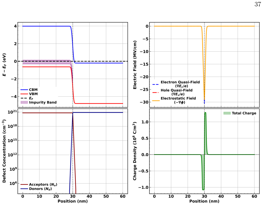
C. J. Wort, R. S. Balmer, Diamond as an electronic material, Materials Today 11 (1) (2008) 22–28. doi:https://doi.org/10.1016/S1369-7021(07) 70349-8. URLhttps://www.sciencedirect.com/science/ article/pii/S1369702107703498 21 Figure 22: Equilibrium PN junction in diamond with a PV-doped P-region and single substitutional phosphorus-doped N-region. Panels s...
-
[2]
J. Isberg, J. Hammersberg, D. Twitchen, A. White- head, Single crystal diamond for electronic ap- plications, Diamond and Related Materials 13 (2) (2004) 320 – 324, carbon Materials for Active Electronics. Proceedings of Symposium L, E-MRS Spring Meeting 2003.doi:https: //doi.org/10.1016/j.diamond.2003.10.017. URLhttp://www.sciencedirect.com/science/ arti...
-
[3]
G. Perez, A. Maréchal, G. Chicot, P. Lefranc, P.- O. Jeannin, D. Eon, N. Rouger, Diamond semi- conductor performances in power electronics ap- plications, Diamond and Related Materials 110 (2020) 108154.doi:https://doi.org/10.1016/j. diamond.2020.108154
work page doi:10.1016/j 2020
-
[4]
M. Panizza, G. Cerisola, Application of diamond electrodes to electrochemical processes, Electrochim- ica Acta 51 (2) (2005) 191–199.doi:https: //doi.org/10.1016/j.electacta.2005.04.023. URLhttps://www.sciencedirect.com/science/ article/pii/S001346860500397X
-
[5]
T. Shimaoka, S. Koizumi, M. M. Tanaka, Di- amond photovoltaic radiation sensor using pn junction, Applied Physics Letters 113 (9) (2018) 093504.arXiv:https://pubs.aip.org/aip/apl/ article-pdf/doi/10.1063/1.5034413/19772003/ 093504\_1\_online.pdf,doi:10.1063/1.5034413. URLhttps://doi.org/10.1063/1.5034413
-
[6]
A. Aleksov, M. Kubovic, N. Kaeb, U. Spitzberg, A. Bergmaier, G. Dollinger, T. Bauer, M. Schreck, B. Stritzker, E. Kohn, Diamond field effect transistors—concepts and challenges, Diamond and Related Materials 12 (3) (2003) 391– 398, 13th European Conference on Diamond, Diamond-Like Materials, Carbon Nanotubes, Nitrides and Silicon Carbide.doi:https: 22 //d...
-
[7]
H. Kato, T. Makino, M. Ogura, D. Takeuchi, S. Yamasaki, Fabrication of bipolar junction transistor on (001)-oriented diamond by utilizing phosphorus-doped n-type diamond base, Diamond and Related Materials 34 (2013) 41–44.doi:https: //doi.org/10.1016/j.diamond.2013.02.004. URLhttps://www.sciencedirect.com/science/ article/pii/S0925963513000277
-
[8]
Y. Gurbuz, O. Esame, I. Tekin, W. P. Kang, J. L. Davidson, Diamond semiconductor tech- nology for rf device applications, Solid-State Electronics 49 (7) (2005) 1055–1070.doi:https: //doi.org/10.1016/j.sse.2005.04.005. URLhttps://www.sciencedirect.com/science/ article/pii/S0038110105001139
-
[9]
D. Eon, A. Traoré, J. Pernot, E. Gheeraert, Re- cent progress on diamond schottky diode, in: 2016 28th International Symposium on Power Semicon- ductor Devices and ICs (ISPSD), 2016, pp. 55–58. doi:10.1109/ISPSD.2016.7520776
-
[10]
V. Jha, H. Surdi, M. Faizan Ahmad, F. Koeck, R. J. Nemanich, S. Goodnick, T. J. Thornton, Diamond schottkyp-i-ndiodesforhighpowerrfreceiverprotec- tors, Solid-State Electronics 186 (2021) 108154.doi: https://doi.org/10.1016/j.sse.2021.108154. URLhttps://www.sciencedirect.com/science/ article/pii/S0038110121001970
-
[11]
M. Suzuki, T. Sakai, T. Makino, H. Kato, D. Takeuchi, M. Ogura, H. Okushi, S. Ya- masaki, Electrical characterization of dia- mond pin diodes for high voltage applica- tions, physica status solidi (a) 210 (10) (2013) 2035–2039.arXiv:https://onlinelibrary. wiley.com/doi/pdf/10.1002/pssa.201300051, doi:https://doi.org/10.1002/pssa.201300051. URLhttps://onli...
-
[12]
, year = 1961, month = mar, journal =
W. Shockley, H. J. Queisser, Detailed Balance Limit of Efficiency of p-n Junction Solar Cells, Journal of Applied Physics 32 (3) (1961) 510–519.doi: 10.1063/1.1736034
-
[13]
A. Luque, A. Martí, Increasing the efficiency of ideal solar cells by photon induced transitions at inter- mediate levels, Physical Review Letters 78 (1997) 5014–5017.doi:10.1103/PhysRevLett.78.5014. URLhttps://link.aps.org/doi/10.1103/ PhysRevLett.78.5014
-
[14]
A. S. Brown, M. A. Green, Impurity pho- tovoltaic effect: Fundamental energy con- version efficiency limits, Journal of Applied Physics 92 (3) (2002) 1329–1336.arXiv: https://pubs.aip.org/aip/jap/article-pdf/ 92/3/1329/19288883/1329\_1\_online.pdf, doi:10.1063/1.1492016. URLhttps://doi.org/10.1063/1.1492016
-
[15]
I. Ramiro, A. Martí, Intermediate band solar cells: Present and future, Progress in Photo- voltaics: Research and Applications 29 (7) (2021) 705–713.arXiv:https://onlinelibrary.wiley. com/doi/pdf/10.1002/pip.3351,doi:https: //doi.org/10.1002/pip.3351. URLhttps://onlinelibrary.wiley.com/doi/ abs/10.1002/pip.3351
- [16]
-
[17]
M. Rasukkannu, D. Velauthapillai, P. Vajeeston, Computational modeling of novel bulk materials for the intermediate-band solar cells, ACS Omega 2 (4) (2017) 1454–1462.doi:10.1021/acsomega.6b00534. URLhttps://doi.org/10.1021/acsomega. 6b00534
-
[18]
M. Kaintz, A. Cammarata, Engineering defect clustering in diamond-based materials for tech- nological applications via quantum mechanical descriptors, Phys. Rev. Appl. 23 (2025) 054029. doi:10.1103/PhysRevApplied.23.054029. URLhttps://link.aps.org/doi/10.1103/ PhysRevApplied.23.054029
-
[19]
S. Heyer, W. Janssen, S. Turner, Y.-G. Lu, W. S. Yeap, J. Verbeeck, K. Haenen, A. Krueger, Toward deep blue nano hope diamonds: heavily boron-doped diamond nanoparticles, ACS Nano 8 (6) (2014) 5757– 5764.doi:10.1021/nn500573x
-
[20]
T. Grotjohn, D. Tran, M. Yaran, S. Demlow, T. Schuelke, Heavy phosphorus doping by epitaxial growth on the (111) diamond surface, Diamond and Related Materials 44 (2014) 129–133.doi:https: //doi.org/10.1016/j.diamond.2014.02.009. URLhttps://www.sciencedirect.com/science/ article/pii/S0925963514000442
-
[21]
J. P. Goss, P. R. Briddon, Theory of boron aggregates in diamond: First-principles calcu- lations, Physical Review B 73 (2006) 085204. doi:10.1103/PhysRevB.73.085204. URLhttps://link.aps.org/doi/10.1103/ PhysRevB.73.085204 23
-
[22]
T. Umeda, K. Watanabe, H. Hara, H. Sumiya, S. On- oda, A. Uedono, I. Chuprina, P. Siyushev, F. Jelezko, J. Wrachtrup, J. Isoya, Negatively charged boron vacancy center in diamond, Physical Review B 105 (2022) 165201.doi:10.1103/PhysRevB.105.165201. URLhttps://link.aps.org/doi/10.1103/ PhysRevB.105.165201
-
[23]
M. Muruganathan, H. Mizuta, Boron vacancy color center in diamond: Ab initio study, Diamond and Related Materials 114 (2021) 108341.doi:https: //doi.org/10.1016/j.diamond.2021.108341. URLhttps://www.sciencedirect.com/science/ article/pii/S0925963521001047
-
[24]
P. Ashcheulov, J. Šebera, A. Kovalenko, V. Petrák, F. Fendrych, M. Nesládek, A. Taylor, Z. Vlčková Živ- cová, O. Frank, L. Kavan, M. Dračínský, P. Hubík, J. Vacík, I. Kraus, I. Kratochvílová, Conduc- tivity of boron-doped polycrystalline diamond films: influence of specific boron defects, The European Physical Journal B 86 (10) (2013) 443. doi:10.1140/epj...
-
[25]
M. N. R. Ashfold, J. P. Goss, B. L. Green, P. W. May, M. E. Newton, C. V. Peaker, Nitrogen in dia- mond, Chemical Reviews 120 (12) (2020) 5745–5794. doi:10.1021/acs.chemrev.9b00518. URLhttps://doi.org/10.1021/acs.chemrev. 9b00518
-
[26]
Ekimov, M
E. Ekimov, M. Kondrin, Vacancy-impurity centers in diamond: perspectives of synthesis and applications, Uspekhi Fizicheskih Nauk 60 (2016).doi:10.3367/ UFNr.2016.11.037959
2016
-
[27]
Y. Makino, T. Mahiko, M. Liu, A. Tsu- rui, T. Yoshikawa, S. Nagamachi, S. Tanaka, K. Hokamoto, M. Ashida, M. Fujiwara, N. Mizuochi, M. Nishikawa, Straightforward synthesis of silicon va- cancy (siv) center-containing single-digit nanometer nanodiamonds via detonation process, Diamond and Related Materials 112 (2021) 108248.doi:https: //doi.org/10.1016/j.d...
-
[28]
J. P. Goss, P. R. Briddon, M. J. Rayson, S. J. Sque, R. Jones, Vacancy-impurity com- plexes and limitations for implantation doping of diamond, Phys. Rev. B 72 (2005) 035214. doi:10.1103/PhysRevB.72.035214. URLhttps://link.aps.org/doi/10.1103/ PhysRevB.72.035214
-
[29]
M. J. Verstraete, J. Abreu, G. Allemand, B. Amadon, G. Antonius, M. Azizi, L. Baguet, C. Barat, L. Bastogne, R. Béjaud, J.-M. Beuken, J. Bieder, A. Blanchet, F. Bottin, J. Bouchet, J. Bouquiaux, E. Bousquet, J. Boust, F. Brieuc, V. Brousseau- Couture, N. Brouwer, F. Bruneval, A. Castellano, E. Castiel, J.-B. Charraud, J. Clérouin, M. Côté, C. Duval, A. Ga...
-
[30]
Thermal-FIST: A package for heavy-ion collisions and hadronic equation of state
X. Gonze, B. Amadon, G. Antonius, F. Arnardi, L. Baguet, J.-M. Beuken, J. Bieder, F. Bottin, J. Bouchet, E. Bousquet, N. Brouwer, F. Bruneval, G. Brunin, T. Cavignac, J.-B. Charraud, W. Chen, M. Côté, S. Cottenier, J. Denier, G. Geneste, P. Ghosez, M. Giantomassi, Y. Gillet, O. Gingras, D. R. Hamann, G. Hautier, X. He, N. Helbig, N. Holzwarth, Y. Jia, F. ...
-
[31]
X. Gonze, G.-M. Rignanese, M. Verstraete, J.-M. Beuken, Y. Pouillon, R. Caracas, F. Jollet, M. Tor- rent, G. Zérah, M. Mikami, P. Ghosez, M. Vei- then, J.-Y. Raty, V. Olevano, F. Bruneval, L. Rein- ing, R. Godby, G. Onida, D. H. D.C. Allan, A brief introduction to the ABINIT software package, Zeitschrift für Kristallographie - Crystalline Materi- als 220 ...
-
[32]
G. Brunin, H. P. C. Miranda, M. Giantomassi, M. Royo, M. Stengel, M. J. Verstraete, X. Gonze, G.- M. Rignanese, G. Hautier, Phonon-limited electron mobility in si, gaas, and gap with exact treatment of dynamical quadrupoles, Phys. Rev. B 102 (2020) 094308.doi:10.1103/PhysRevB.102.094308. 24 URLhttps://link.aps.org/doi/10.1103/ PhysRevB.102.094308
-
[33]
A. Cammarata, M. Kaintz, T. Polcar, Engineering width and directness of the band gap in diamond- based materials: An ab initio investigation towards electron-structure features control, Diamond and Related Materials 128 (2022) 109237.doi:https: //doi.org/10.1016/j.diamond.2022.109237. URLhttps://www.sciencedirect.com/science/ article/pii/S0925963522004198
-
[34]
Z. Wu, R. E. Cohen, More accurate generalized gradient approximation for solids, Phys. Rev. B 73 (2006) 235116.doi:10.1103/PhysRevB.73.235116. URLhttps://link.aps.org/doi/10.1103/ PhysRevB.73.235116
-
[35]
H. J. Monkhorst, J. D. Pack, Special points for brillouin-zone integrations, Phys. Rev. B 13 (1976) 5188–5192.doi:10.1103/PhysRevB.13.5188. URLhttps://link.aps.org/doi/10.1103/ PhysRevB.13.5188
-
[36]
N. Bindzus, T. Straasø, N. Wahlberg, J. Becker, L. Bjerg, N. Lock, A.-C. Dippel, B. B. Iversen, Exper- imental determination of core electron deformation in diamond, Acta Crystallographica Section A 70 (1) (2014) 39–48.doi:10.1107/S2053273313026600. URLhttps://doi.org/10.1107/ S2053273313026600
-
[37]
S. Gao, Band gaps and dielectric functions of cu- bic and hexagonal diamond polytypes calculated by many-body perturbation theory, physica status solidi (b) 252 (09 2014).doi:10.1002/pssb.201451197
-
[38]
F. Belviso, V. E. P. Claerbout, A. Comas-Vives, N. S. Dalal, F.-R. Fan, A. Filippetti, V. Fioren- tini, L. Foppa, C. Franchini, B. Geisler, L. M. Ghiringhelli, A. Groß, S. Hu, J. Íñiguez, S. K. Kauwe, J. L. Musfeldt, P. Nicolini, R. Pentcheva, T. Polcar, W. Ren, F. Ricci, F. Ricci, H. S. Sen, J. M. Skelton, T. D. Sparks, A. Stroppa, A. Urru, M. Vandichel,...
-
[39]
L. Hedin, New method for calculating the one-particle green’s function with application to the electron- gas problem, Phys. Rev. 139 (1965) A796–A823. doi:10.1103/PhysRev.139.A796. URLhttps://link.aps.org/doi/10.1103/ PhysRev.139.A796
-
[40]
R. W. Godby, R. J. Needs, Metal-insulator transi- tion in Kohn–Sham theory and quasiparticle theory, Phys. Rev. Lett. 62 (10) (1989) 1169–1172.doi: 10.1103/physrevlett.62.1169. URLhttps://doi.org/10.1103/physrevlett.62. 1169
-
[41]
S. Sharma, C. Ambrosch-Draxl, Second- harmonic optical response from first princi- ples, Physica Scripta 2004 (T109) (2004) 128. doi:10.1238/Physica.Topical.109a00128. URLhttps://doi.org/10.1238/Physica. Topical.109a00128
-
[42]
S. Poncé, W. Li, S. Reichardt, F. Giustino, First-principles calculations of charge carrier mobility and conductivity in bulk semiconduc- tors and two-dimensional materials, Reports on Progress in Physics 83 (3) (2020) 036501. doi:10.1088/1361-6633/ab6a43. URLhttps://doi.org/10.1088/1361-6633/ ab6a43
-
[43]
A. Togo, L. Chaput, I. Tanaka, Distributions of phonon lifetimes in brillouin zones, Phys. Rev. B 91 (2015) 094306.doi:10.1103/PhysRevB.91.094306
-
[44]
A. Togo, L. Chaput, T. Tadano, I. Tanaka, Imple- mentation strategies in phonopy and phono3py, J. Phys. Condens. Matter 35 (35) (2023) 353001.doi: 10.1088/1361-648X/acd831
-
[45]
Chaput, Direct solution to the linearized phonon boltzmann equation, Phys
L. Chaput, Direct solution to the linearized phonon boltzmann equation, Phys. Rev. Lett. 110 (2013) 265506.doi:10.1103/PhysRevLett.110.265506. URLhttps://link.aps.org/doi/10.1103/ PhysRevLett.110.265506
-
[46]
A. Gali, M. Fyta, E. Kaxiras, Ab initio su- percell calculations on nitrogen-vacancy center in diamond: Electronic structure and hyper- fine tensors, Phys. Rev. B 77 (2008) 155206. doi:10.1103/PhysRevB.77.155206. URLhttps://link.aps.org/doi/10.1103/ PhysRevB.77.155206
-
[47]
K. Czelej, M. R. Zemła, P. Kamińska, P. Śpiewak, K. J. Kurzydłowski, Clustering of hydrogen, phos- phorus, and vacancies in diamond: A density functional theory analysis, Phys. Rev. B 98 (2018) 075208.doi:10.1103/PhysRevB.98.075208. URLhttps://link.aps.org/doi/10.1103/ PhysRevB.98.075208
-
[48]
M. Verstraete, X. Gonze, Smearing scheme for finite-temperature electronic-structure cal- culations, Phys. Rev. B 65 (2001) 035111. 25 doi:10.1103/PhysRevB.65.035111. URLhttps://link.aps.org/doi/10.1103/ PhysRevB.65.035111
-
[49]
C. Freysoldt, B. Grabowski, T. Hickel, J. Neuge- bauer, G. Kresse, A. Janotti, C. G. Van de Walle, First-principles calculations for point defects in solids, Rev. Mod. Phys. 86 (2014) 253–305. doi:10.1103/RevModPhys.86.253. URLhttps://link.aps.org/doi/10.1103/ RevModPhys.86.253
-
[50]
D. Zhang, X. Sun, Y. Zhang, C. Cheng, Y. Guo, Z. Gan, S. Liu, Y. Hao, Theoretical study of n- type diamond with li doping and li-b co-doping: A density functional simulation, Diamond and Related Materials 131 (2023) 109544.doi:https: //doi.org/10.1016/j.diamond.2022.109544. URLhttps://www.sciencedirect.com/science/ article/pii/S0925963522007269
-
[51]
N. Gao, L. Gao, H. Yu, First-principles study of n and s co-doping in diamond, Diamond and Related Materials 132 (2023) 109651.doi:https: //doi.org/10.1016/j.diamond.2022.109651. URLhttps://www.sciencedirect.com/science/ article/pii/S0925963522008330
-
[52]
I. Aharonovich, S. Castelletto, D. A. Simp- son, C.-H. Su, A. D. Greentree, S. Prawer, Diamond-based single-photon emitters, Reports on Progress in Physics 74 (7) (2011) 076501. doi:10.1088/0034-4885/74/7/076501. URLhttps://dx.doi.org/10.1088/0034-4885/ 74/7/076501
-
[53]
A. Gali, J. R. Maze, Ab initio study of the split silicon-vacancy defect in diamond: Electronic struc- ture and related properties, Phys. Rev. B 88 (2013) 235205.doi:10.1103/PhysRevB.88.235205. URLhttps://link.aps.org/doi/10.1103/ PhysRevB.88.235205
-
[54]
W. Setyawan, S. Curtarolo, High-throughput electronic band structure calculations: Chal- lenges and tools, Computational Materials Science 49 (2) (2010) 299–312.doi:https: //doi.org/10.1016/j.commatsci.2010.05.010. URLhttps://www.sciencedirect.com/science/ article/pii/S0927025610002697
-
[55]
C. Gueymard, D. Myers, K. Emery, Proposed refer- ence irradiance spectra for solar energy systems test- ing, Solar Energy 73 (6) (2002) 443–467.doi:https: //doi.org/10.1016/S0038-092X(03)00005-7. URLhttps://www.sciencedirect.com/science/ article/pii/S0038092X03000057
-
[56]
G. Onida, L. Reining, A. Rubio, Electronic ex- citations: density-functional versus many-body green’s-function approaches, Rev. Mod. Phys. 74 (2002) 601–659.doi:10.1103/RevModPhys.74.601. URLhttps://link.aps.org/doi/10.1103/ RevModPhys.74.601
-
[57]
Neamen, Semiconductor Physics And Devices, 3rd Edition, McGraw-Hill, Inc., USA, 2002, iSBN: 0-07- 232107-5
D. Neamen, Semiconductor Physics And Devices, 3rd Edition, McGraw-Hill, Inc., USA, 2002, iSBN: 0-07- 232107-5
2002
-
[58]
A. Kanevce, M. O. Reese, T. M. Barnes, S. A. Jensen, W. K. Metzger, The roles of carrier concentration and interface, bulk, and grain-boundary recombina- tion for 25% efficient cdte solar cells, Journal of Ap- plied Physics 121 (21) (2017) 214506.doi:10.1063/ 1.4984320. URLhttps://doi.org/10.1063/1.4984320
-
[59]
S. D. Stranks, H. J. Snaith, Metal-halide perovskites for photovoltaic and light-emitting devices, Nature Nanotechnology 10 (5) (2015) 391–402.doi:10. 1038/nnano.2015.90. URLhttps://doi.org/10.1038/nnano.2015.90
-
[60]
Kittel, Introduction to Solid State Physics, John Wiley & Sons Inc., 2015, iSBN: 978-81-265-3518-7
C. Kittel, Introduction to Solid State Physics, John Wiley & Sons Inc., 2015, iSBN: 978-81-265-3518-7
2015
-
[61]
P. G. Klemens, The scattering of low-frequency lattice waves by static imperfections, Proceedings of the Physical Society. Section A 68 (12) (1955) 1113. doi:10.1088/0370-1298/68/12/303. URLhttps://doi.org/10.1088/0370-1298/68/ 12/303
-
[62]
Callaway, Model for lattice thermal conductivity at low temperatures, Phys
J. Callaway, Model for lattice thermal conductivity at low temperatures, Phys. Rev. 113 (1959) 1046–1051. doi:10.1103/PhysRev.113.1046. URLhttps://link.aps.org/doi/10.1103/ PhysRev.113.1046
-
[63]
N. A. Katcho, J. Carrete, W. Li, N. Mingo, Effect of nitrogen and vacancy defects on the thermal conductivity of diamond: An ab initio green’s function approach, Phys. Rev. B 90 (2014) 094117. doi:10.1103/PhysRevB.90.094117. URLhttps://link.aps.org/doi/10.1103/ PhysRevB.90.094117
-
[64]
D. Chen, S. Li, B. Li, P. Guo, Thermal trans- port in metal halide perovskites and other third- generation photovoltaic materials, Applied Physics Reviews 11 (4) (2024) 041311.doi:10.1063/5. 0226632. URLhttps://doi.org/10.1063/5.0226632
work page doi:10.1063/5 2024
-
[65]
A. C. Pakpour-Tabrizi, A. K. Schenk, A. J. U. Holt, S. K. Mahatha, F. Arnold, M. Bianchi, R. B. Jack- man, J. E. Butler, A. Vikharev, J. A. Miwa, P. Hof- mann, S. P. Cooil, J. W. Wells, F. Mazzola, The oc- cupied electronic structure of ultrathin boron doped diamond, Nanoscale Adv. 2 (2020) 1358–1364.doi: 26 10.1039/C9NA00593E. URLhttp://dx.doi.org/10.103...
-
[66]
I.-T. Lu, J.-J. Zhou, J. Park, M. Bernardi, First-principles ionized-impurity scatter- ing and charge transport in doped materi- als, Phys. Rev. Mater. 6 (2022) L010801. doi:10.1103/PhysRevMaterials.6.L010801. URLhttps://link.aps.org/doi/10.1103/ PhysRevMaterials.6.L010801
-
[67]
J. Leveillee, X. Zhang, E. Kioupakis, F. Giustino, Ab initio calculation of carrier mobility in semiconductors including ionized-impurity scattering, Phys. Rev. B 107 (2023) 125207. doi:10.1103/PhysRevB.107.125207. URLhttps://link.aps.org/doi/10.1103/ PhysRevB.107.125207 27 From Defects to Devices: Design Guidelines for High-Performance Diamond-Based Sola...
-
[68]
Setyawan and S
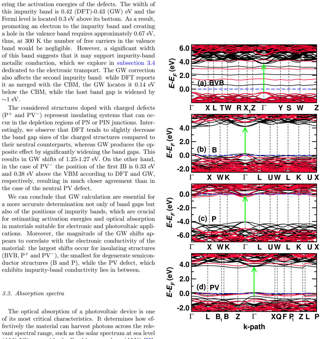
W. Setyawan and S. Curtarolo, High-throughput electronic band structure calculations: Chal- lenges and tools, Computational Materials Science 49, 299 (2010). 31 Γ X W K Γ L U W L K U X k-path -2.0 0.0 2.0 4.0 E-EF (eV) (b) -2.0 0.0 2.0 4.0 E-EF (eV) P + (d) -2.0 0.0 2.0 4.0 E-EF (eV) 0.0 2.0 4.0 6.0E-EF (eV) (c) (a) PV BVB PV - FIG. 1. Electronic band str...
2010
discussion (0)
Sign in with ORCID, Apple, or X to comment. Anyone can read and Pith papers without signing in.