Recognition: no theorem link
A Microfabricated PCM-Switched Reconfigurable Intelligent Surface for Wideband Millimeter-Wave Beam Steering
Pith reviewed 2026-05-11 01:06 UTC · model grok-4.3
The pith
Microfabricated VO2-switched RIS delivers 10-20 dB gain for dynamic beam steering up to 60 degrees over 18 percent bandwidth at 33 GHz
A machine-rendered reading of the paper's core claim, the machinery that carries it, and where it could break.
Core claim
The central claim is that monolithically integrating VO2 switches into a 10 x 20 array of unit cells approximately one-fifth of a wavelength in size, with serial biasing per column, produces programmable spatial phase profiles that steer millimeter-wave beams up to 60 degrees while delivering measured far-field gain enhancements of 10-20 dB across an 18 percent fractional bandwidth centered at 33 GHz, with patterns matching semi-numerical channel model predictions.
What carries the argument
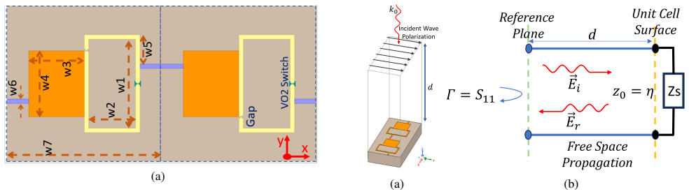
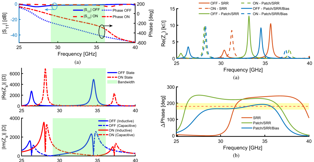
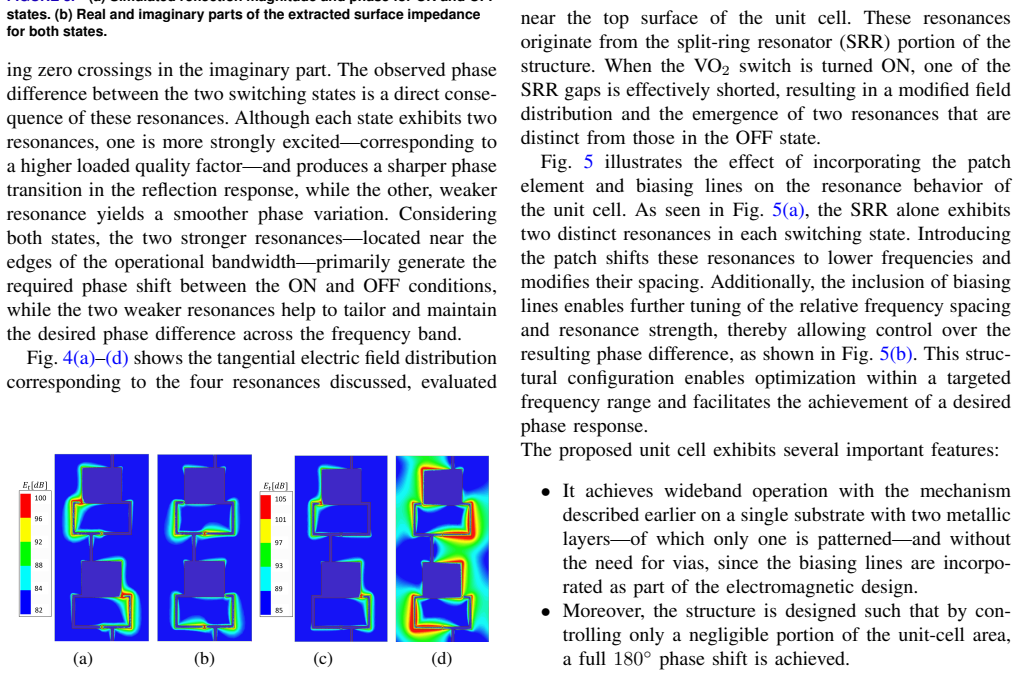
The VO2 switch elements embedded within each subwavelength unit cell, whose electrically actuated resistance change modulates the local surface impedance to set the reflection phase and amplitude.
Load-bearing premise
That the serial column biasing and full-wave surface-impedance simulations will produce uniform phase control and low-loss behavior across the full fabricated 10x20 array without significant degradation from fabrication variations or unaccounted parasitics.
What would settle it
Fabricating and measuring the 10x20 array in the far field at 33 GHz and observing gain enhancement below 10 dB at steering angles near 60 degrees due to phase non-uniformity across the surface.
Figures


read the original abstract
This paper presents the design, fabrication, and experimental validation of a reconfigurable intelligent surface (RIS) employing electrically actuated vanadium dioxide (VO2) switches for millimeter wave beam steering. The proposed RIS is realized using a multilayer microfabrication process on an alumina substrate, enabling monolithic integration of hundreds of sub-4 micrometer VO2 switching elements within deeply subwavelength unit cells, approximately one-fifth of the wavelength. The switching-induced modulation of surface impedance is analyzed through full-wave simulations, and the resulting phase and amplitude responses are experimentally characterized using a custom WR-28 waveguide measurement setup. Based on the validated unit-cell design, a 10 x 20 RIS array integrating 200 VO2 switches is fabricated. The switches within each column are serially biased using integrated routing lines, allowing programmable control of the spatial phase distribution across the surface. Synthesized phase profiles enable dynamic beam steering, resulting in measured far-field gain enhancement of 10-20 dB over an 18 percent fractional bandwidth centered at 33 GHz, with steering angles up to 60 degrees. The measured radiation patterns are in good agreement with semi-numerical channel modeling predictions. By combining thin-film PCM switching with an integration-aware unit-cell design, this work demonstrates a scalable RIS architecture that mitigates packaging parasitics and footprint limitations inherent to conventional semiconductor-based implementations, providing a practical pathway toward higher-frequency reconfigurable surfaces.
Editorial analysis
A structured set of objections, weighed in public.
Referee Report
Summary. The manuscript presents the design, microfabrication on alumina, and experimental validation of a 10×20 reconfigurable intelligent surface (RIS) employing 200 monolithically integrated vanadium dioxide (VO2) switches within deeply subwavelength (~λ/5) unit cells. Serial column biasing via integrated routing enables programmable phase profiles. Unit-cell impedance modulation is analyzed via full-wave simulations and characterized in a WR-28 waveguide setup. Synthesized profiles yield measured far-field gain enhancement of 10–20 dB over an 18% fractional bandwidth at 33 GHz with steering up to 60°, in agreement with semi-numerical modeling. The work claims a scalable PCM-based RIS architecture that mitigates conventional switch parasitics.
Significance. If the measured performance is robustly verified, the result is significant for millimeter-wave RIS technology. It demonstrates monolithic integration of hundreds of sub-4 μm VO2 elements in a practical array, providing a pathway to higher-frequency reconfigurable surfaces without packaging-induced parasitics. Credit is due for the experimental waveguide validation of the unit cell combined with array-level far-field steering data and modeling agreement.
major comments (2)
- [Array fabrication and biasing] § on array fabrication and biasing: The headline claim of 10–20 dB gain enhancement and 60° steering assumes that serial column biasing and unit-cell full-wave simulations produce uniform phase control across the 10×20 array. No array-level reflection-phase measurements, bias-line de-embedding, or quantification of fabrication spread/parasitics are provided; phase deviations of even 20–30° would degrade the far-field pattern below the modeled prediction, directly undermining the central performance numbers.
- [Experimental results] Experimental results section: The reported far-field gain enhancements of 10–20 dB and radiation patterns are presented without error bars, raw data traces, repeatability statistics, or explicit exclusion criteria. This renders the central experimental claim plausible but not fully verifiable from the provided data, weakening confidence that the measured enhancement matches the semi-numerical model under realistic conditions.
minor comments (2)
- [Abstract] The abstract states 'good agreement' with modeling but omits quantitative metrics (e.g., RMS phase error or pattern correlation) that would strengthen the comparison.
- [Figures] Figure captions for far-field patterns could explicitly note the number of independent measurements averaged and any normalization applied.
Simulated Author's Rebuttal
We thank the referee for the constructive comments and the recognition of the significance of our monolithic VO2-based RIS demonstration. We address the major comments point by point below, offering clarifications and revisions to improve verifiability without altering the core experimental claims.
read point-by-point responses
-
Referee: [Array fabrication and biasing] § on array fabrication and biasing: The headline claim of 10–20 dB gain enhancement and 60° steering assumes that serial column biasing and unit-cell full-wave simulations produce uniform phase control across the 10×20 array. No array-level reflection-phase measurements, bias-line de-embedding, or quantification of fabrication spread/parasitics are provided; phase deviations of even 20–30° would degrade the far-field pattern below the modeled prediction, directly undermining the central performance numbers.
Authors: We agree that array-level reflection-phase measurements would provide direct evidence of uniformity. Such measurements were not performed because they require specialized large-aperture near-field scanning equipment not available in our setup; the WR-28 waveguide characterization was limited to single unit cells. The semi-numerical model incorporates the serial column biasing topology and assumes phase uniformity based on the monolithic fabrication process on alumina, which was designed to minimize parasitics. The measured far-field patterns agree with this model across steering angles and bandwidth, providing indirect validation. In revision we will add a dedicated paragraph quantifying expected fabrication spread (from process tolerances) and its simulated impact on array factor, plus a note on the absence of direct array phase data as a limitation. revision: partial
-
Referee: [Experimental results] Experimental results section: The reported far-field gain enhancements of 10–20 dB and radiation patterns are presented without error bars, raw data traces, repeatability statistics, or explicit exclusion criteria. This renders the central experimental claim plausible but not fully verifiable from the provided data, weakening confidence that the measured enhancement matches the semi-numerical model under realistic conditions.
Authors: The referee correctly identifies that the current presentation lacks statistical detail. The reported 10–20 dB enhancements and patterns are averages from repeated chamber measurements performed on the same device; however, these statistics were not included in the original manuscript. In the revised version we will add error bars (standard deviation from at least three independent alignments), include representative raw S-parameter and pattern traces as supplementary material, and explicitly state the measurement protocol and exclusion criteria (e.g., alignment tolerance). These additions will make the agreement with the semi-numerical model more transparent without changing the reported performance numbers. revision: yes
Circularity Check
No circularity: experimental validation of fabricated RIS with measured results
full rationale
The paper reports design, microfabrication, unit-cell full-wave simulation, and direct far-field measurements on a 10x20 array. All load-bearing claims (10-20 dB gain, 60° steering, 18% bandwidth) are tied to physical measurements rather than any derivation, fitted parameter, or self-citation chain. No equations are presented that reduce a claimed result to its own inputs by construction; the serial biasing and phase synthesis are implementation details validated by experiment, not mathematical self-reference.
Axiom & Free-Parameter Ledger
Reference graph
Works this paper leans on
-
[1]
Reconfigurable intelligent surfaces for energy efficiency in wireless communication,
C. Huang, A. Zappone, G. C. Alexandropoulos, M. Debbah, and C. Yuen, “Reconfigurable intelligent surfaces for energy efficiency in wireless communication,”IEEE Trans. Wireless Commun., vol. 18, no. 8, pp. 4157–4170, 2019
work page 2019
-
[2]
M. D. Renzo, A. Zappone, M. Debbah, M.-S. Alouini, C. Yuen, J. de Rosny, and S. Tretyakov, “Smart radio environments empowered by reconfigurable intelligent surfaces: How it works, state of research, and the road ahead,”IEEE J. Sel. Areas Commun., vol. 38, no. 11, pp. 2450–2525, 2020
work page 2020
-
[3]
E. Basar, G. C. Alexandropoulos, Y . Liu, Q. Wu, S. Jin, C. Yuen, O. A. Dobre, and R. Schober, “Reconfigurable intelligent surfaces for 6g: Emerging hardware architectures, applications, and open challenges,” IEEE V ehicular Technology Magazine, vol. 19, no. 3, pp. 27–47, 2024
work page 2024
-
[4]
Metasurfaces: From microwaves to visible,
S. B. Glybovski, S. A. Tretyakov, P. A. Belov, Y . S. Kivshar, and C. R. Simovski, “Metasurfaces: From microwaves to visible,”Phys. Rep., vol. 634, pp. 1–72, 2016
work page 2016
-
[5]
A wideband reconfig- urable intelligent surface for 5G millimeter-wave applications,
R. Wang, Y . Yang, B. Makki, and A. Shamim, “A wideband reconfig- urable intelligent surface for 5G millimeter-wave applications,”IEEE Trans. Antennas Propag., vol. 72, no. 3, pp. 2399–2410, 2024
work page 2024
-
[6]
A. Araghi, M. Khalily, M. Safaei, A. Bagheri, V . Singh, F. Wang, and R. Tafazolli, “Reconfigurable intelligent surface (RIS) in the sub- 6 GHz band: Design, implementation, and real-world demonstration,” IEEE Access, vol. 10, pp. 2646–2655, 2022
work page 2022
-
[7]
A. Palomares-Caballero, M. P ´erez-Escribano, C. Molero, P. Padilla, M. Garc´ıa-Vigueras, and R. Gillard, “Broadband 1-bit reconfigurable intelligent surface at millimeter waves: Overcoming PIN-diode degra- dation with slotline ring topology,”IEEE Trans. Antennas Propag., 2025
work page 2025
-
[8]
An E-band reconfigurable reflectar- ray antenna using PIN diodes for millimeter-wave communications,
C. Liu, F. Yang, S. Xu, and M. Li, “An E-band reconfigurable reflectar- ray antenna using PIN diodes for millimeter-wave communications,” IEEE Trans. Antennas Propag., vol. 71, no. 8, pp. 6924–6929, 2023
work page 2023
-
[9]
60-GHz electronically reconfigurable large reflectarray using single- bit phase shifters,
H. Kamoda, T. Iwasaki, J. Tsumochi, T. Kuki, and O. Hashimoto, “60-GHz electronically reconfigurable large reflectarray using single- bit phase shifters,”IEEE Trans. Antennas Propag., vol. 59, no. 7, pp. 2524–2531, 2011
work page 2011
-
[10]
A 2-bit wideband 5G mm-wave RIS with low sidelobe levels and no quantization lobe,
R. Wang, Y . Yang, and A. Shamim, “A 2-bit wideband 5G mm-wave RIS with low sidelobe levels and no quantization lobe,”IEEE Trans. Antennas Propag., vol. 73, no. 12, pp. 10 042–10 056, 2025
work page 2025
-
[11]
Review paper on hardware of reconfigurable intelligent surfaces,
B. Rana, S.-S. Cho, and I.-P. Hong, “Review paper on hardware of reconfigurable intelligent surfaces,”IEEE Access, vol. 11, pp. 29 614– 29 634, 2023
work page 2023
-
[12]
S-band GaAs FET reconfig- urable reflectarray for passive communications,
R. L. Schmid, D. B. Shrekenhamer, O. F. Somerlock, A. C. Malone, T. A. Sleasman, and R. S. Awadallah, “S-band GaAs FET reconfig- urable reflectarray for passive communications,” inProc. IEEE Radio Wireless Symp. (RWS). IEEE, 2020, pp. 91–93
work page 2020
-
[13]
X. Chen, N. M. Monroe, G. C. Dogiamis, R. A. Stingel, P. Myers, and R. Han, “A 265-GHz CMOS reflectarray with 98×98 elements for 1◦- wide beam forming and high-angular-resolution radar imaging,”IEEE J. Solid-State Circuits, vol. 59, no. 11, pp. 3655–3669, 2024
work page 2024
-
[14]
A wideband GaAs phase-reconfigurable reflector for K-band reflectarray antenna,
Y . Yan, Y . Xiao, F. Lin, K. Zhu, W. Wang, H. Tao, and H. Sun, “A wideband GaAs phase-reconfigurable reflector for K-band reflectarray antenna,”IEEE Microw. Wireless Technol. Lett., pp. 1–4, 2025
work page 2025
-
[15]
G. M. Rebeiz,RF MEMS: Theory, Design, and Technology. Hoboken, NJ, USA: John Wiley & Sons, 2004
work page 2004
-
[16]
Beam switching reflectarray monolithically integrated with RF MEMS switches,
O. Bayraktar, ¨O. A. Civi, and T. Akin, “Beam switching reflectarray monolithically integrated with RF MEMS switches,”IEEE Trans. Antennas Propag., vol. 60, no. 2, pp. 854–862, 2012
work page 2012
-
[17]
W-band beam-steerable MEMS-based reflectarray,
S. Montori, E. Chiuppesi, P. Farinelli, L. Marcaccioli, R. V . Gatti, and R. Sorrentino, “W-band beam-steerable MEMS-based reflectarray,” Int. J. Microw. Wireless Technol., vol. 3, no. 5, pp. 521–532, 2011
work page 2011
-
[18]
Reconfigurable unit cell design using MEMS actuator for beam-steering applications,
J. Tayebpour and R. R. Mansour, “Reconfigurable unit cell design using MEMS actuator for beam-steering applications,”IEEE Trans. Antennas Propag., vol. 73, no. 3, pp. 1346–1354, 2025
work page 2025
-
[19]
RF MEMS actuated reconfigurable reflectarray patch-slot element,
H. Rajagopalan, Y . Rahmat-Samii, and W. A. Imbriale, “RF MEMS actuated reconfigurable reflectarray patch-slot element,”IEEE Trans. Antennas Propag., vol. 56, no. 12, pp. 3689–3699, 2008
work page 2008
-
[20]
A review of phase-change materials and their potential for reconfigurable intelligent surfaces,
R. Matos and N. Pala, “A review of phase-change materials and their potential for reconfigurable intelligent surfaces,”Micromachines, vol. 14, no. 6, p. 1259, 2023
work page 2023
-
[21]
D. E. Anagnostou, D. Torres, T. S. Teeslink, and N. Sepulveda, “Vanadium dioxide for reconfigurable antennas and microwave de- vices: Enabling RF reconfigurability through smart materials,”IEEE Antennas Propag. Mag., vol. 62, no. 3, pp. 58–73, 2020
work page 2020
-
[22]
E. Haddad, R. V . Kruzelecky, P. Murzionak, W. Jamroz, K. Tagziria, M. Chaker, and B. Ledrogoff, “Review of the VO 2 smart material applications with emphasis on its use for spacecraft thermal control,” Front. Mater ., vol. 9, p. 1013848, 2022
work page 2022
-
[23]
Reconfigurable SAW res- onators and tunable filters using monolithically integrated VO 2 switches,
A. F. Azarnaminy and R. R. Mansour, “Reconfigurable SAW res- onators and tunable filters using monolithically integrated VO 2 switches,”IEEE Trans. Microw. Theory Techn., vol. 71, no. 1, pp. 181–192, 2023
work page 2023
-
[24]
Novel high-speed PCM switch based on vanadium dioxide with less than 500 ns switching time,
T. G. Williamson and N. Ghalichechian, “Novel high-speed PCM switch based on vanadium dioxide with less than 500 ns switching time,”IEEE Microw. Wireless Technol. Lett., 2025
work page 2025
-
[25]
Electronically-controlled beam-steering through vanadium dioxide metasurfaces,
M. R. M. Hashemi, S.-H. Yang, T. Wang, N. Sep´ulveda, and M. Jarrahi, “Electronically-controlled beam-steering through vanadium dioxide metasurfaces,”Sci. Rep., vol. 6, no. 1, p. 35439, 2016
work page 2016
-
[26]
Y . Yang, M. Vaseem, R. Wang, B. Makki, and A. Shamim, “A fully screen-printed vanadium-dioxide switch-based wideband recon- figurable intelligent surface for 5G and beyond,”IEEE Trans. Microw. Theory Techn., 2025
work page 2025
-
[27]
E. Park, J. Kim, M. Lee, R. Phon, M. Kim, S. Hong, and S. Lim, “Low- cost large-area 100-GHz intelligent reflective surface: electrically col- umn control of screen-printable high phase-changing-ratio vanadium dioxide,”Nanophotonics, vol. 14, no. 9, pp. 1375–1389, 2025
work page 2025
-
[28]
J. A. Ramsey, S. Y . Lee, W. R. Disharoon, D. L. West, and N. Ghalichechian, “Low-loss vanadium dioxide-enabled mmwave tun- able reflective electromagnetic surface with complementary unit cells for wave manipulation,”J. Appl. Phys., vol. 135, no. 21, 2024
work page 2024
-
[29]
A novel RIS unit cell design enabling seamless integration with VO 2 switches,
A. Hojjati-Firoozabadi and R. Mansour, “A novel RIS unit cell design enabling seamless integration with VO 2 switches,” inProc. Eur . Microw. Conf. (EuMC), 2024, pp. 896–899. 16
work page 2024
-
[30]
A. Hojjati-Firoozabadi and R. R. Mansour, “A novel wide-band unit cell design for monolithic integration with electric-field-induced VO 2 switches,” inProc. IEEE Int. Symp. Antennas Propag. and USNC- URSI Radio Sci. Meeting (AP-S/USNC-URSI), 2024, pp. 1869–1870
work page 2024
-
[31]
S. Liu, T. J. Cui, L. Zhang, Q. Xu, Q. Wang, X. Wan, J. Q. Gu, W. X. Tang, M. Q. Qi, and J. G. Han, “Convolution operations on coding metasurface to reach flexible and continuous controls of terahertz beams,”Adv. Sci., vol. 3, no. 10, p. 1600156, 2016
work page 2016
-
[32]
Suppression of quantiza- tion lobes in 1-bit reconfigurable intelligent surfaces,
D. Vabichevich, A. Belov, and A. Sayanskiy, “Suppression of quantiza- tion lobes in 1-bit reconfigurable intelligent surfaces,”IEEE Antennas Wireless Propag. Lett., vol. 22, no. 12, pp. 2808–2811, 2023
work page 2023
-
[33]
L. Wang, Y .-Q. Hao, W. Ma, and S. Liang, “Improving phase transition temperature of VO 2 via Ge doping: a combined experimental and theoretical study,”Rare Met., vol. 40, no. 5, pp. 1337–1346, 2021
work page 2021
-
[34]
Elevated transition temperature in Ge doped VO 2 thin films,
A. Krammer, A. Magrez, W. A. Vitale, P. Mocny, P. Jeanneret, E. Guibert, H. J. Whitlow, A. M. Ionescu, and A. Sch ¨uler, “Elevated transition temperature in Ge doped VO 2 thin films,”J. Appl. Phys., vol. 122, no. 4, 2017. 17
work page 2017
discussion (0)
Sign in with ORCID, Apple, or X to comment. Anyone can read and Pith papers without signing in.