Recognition: 2 theorem links
· Lean TheoremDesign and Characterization of Racetrack 3D-Trench Silicon Sensor Based on 8-Inch Process with Excellent Time Resolution
Pith reviewed 2026-05-11 01:44 UTC · model grok-4.3
The pith
A racetrack 3D-trench silicon sensor with continuous electrodes achieves uniform fields and 50 ps time resolution.
A machine-rendered reading of the paper's core claim, the machinery that carries it, and where it could break.
Core claim
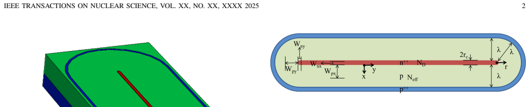
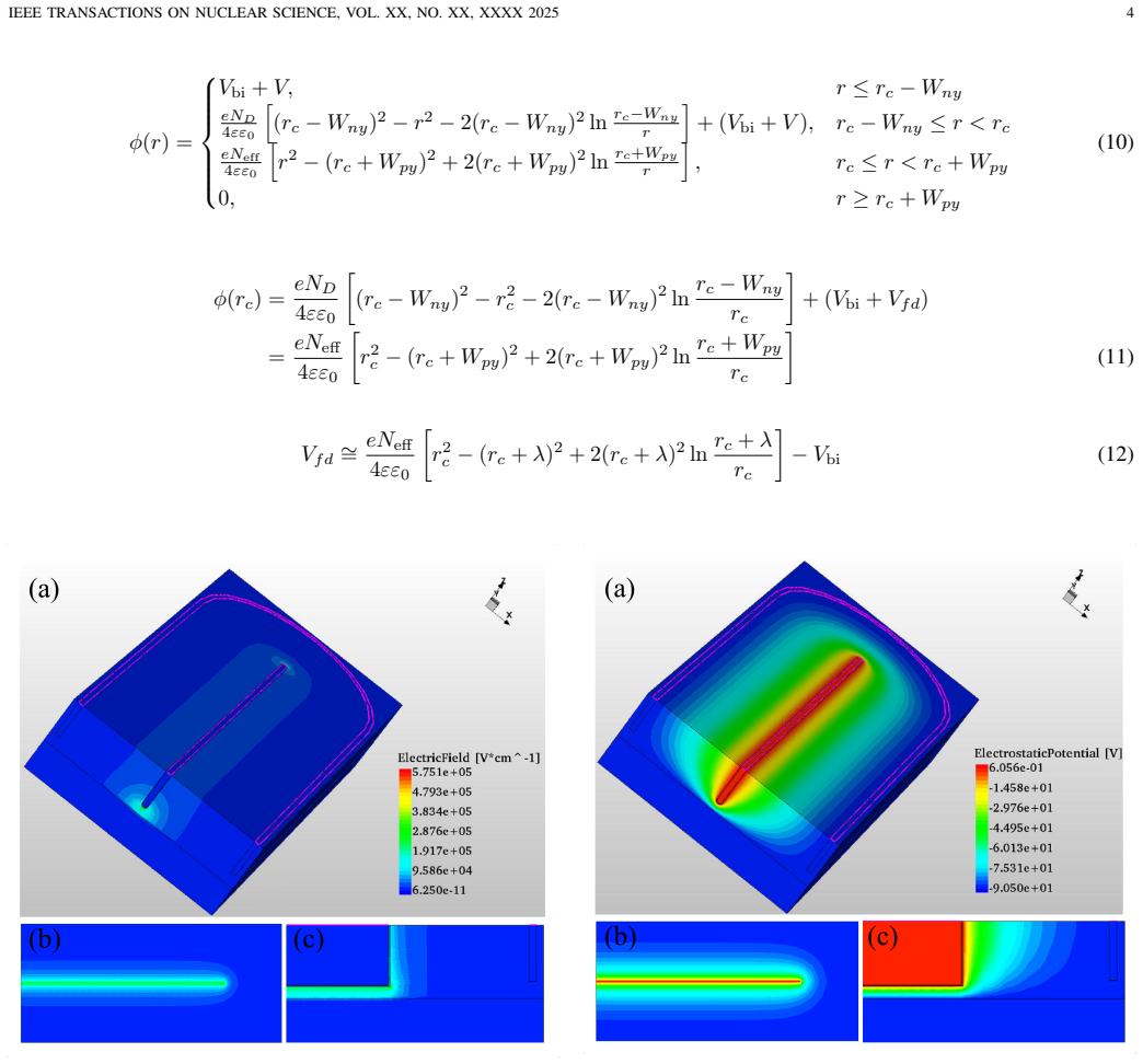
The racetrack 3D-trench silicon sensor uses continuous racetrack electrodes surrounding a long central collection electrode to eliminate electric-field saddle points and low-field regions that appear in columnar or square-cell designs. Fabricated for the first time on an 8-inch platform with 23-micron shallow trenches, the device was evaluated with 3D TCAD simulations, I-V and C-V measurements, and transient current technique (TCT) tests, yielding leakage current below 0.2 nA, breakdown voltage above 110 V, full depletion at a few volts, capacitance as low as 650 fF, collected charge of 4 fC, time response of about 640 ps, and time resolution of 50 ps.
What carries the argument
Racetrack electrode geometry consisting of continuous racetrack-shaped trenches surrounding a central collection electrode, which maintains a more uniform electric field across the sensor volume.
If this is right
- The sensor can be produced at industrial 8-inch scale for cost-effective deployment in large detector systems.
- Shortened collection distances combined with uniform fields support radiation hardness needed for high-luminosity collider environments.
- Low capacitance and fast response enable high-event-rate 4D tracking without sacrificing timing precision.
- Shallow-etch fabrication opens a path to integration with readout electronics on the same wafer.
Where Pith is reading between the lines
- If the field uniformity persists after heavy irradiation, the design could replace planar sensors in timing layers where both position and arrival time must be measured to high accuracy.
- The 23-micron shallow etch may reduce material budget enough to allow the sensor to sit closer to the interaction point than deeper-etched 3D devices.
- Mass-production compatibility suggests the geometry could be adapted for portable radiation monitors outside high-energy physics.
Load-bearing premise
The racetrack geometry fully removes saddle points and low-field regions in real fabricated devices under operational bias and radiation, not only in simulations.
What would settle it
TCT or two-photon-absorption scans that reveal charge-collection efficiency varying by more than 10 percent across the active volume, or time resolution degrading below 100 ps after moderate irradiation, would falsify the uniformity claim.
Figures


read the original abstract
In the extreme environments of high-luminosity colliders, traditional planar silicon sensors suffer severe radiation-induced performance degradation and fail to satisfy the stringent demands of high-precision tracking and high-speed timing in particle physics. 3D silicon sensors enhance radiation hardness by shortening charge collection distance, yet conventional designs with columnar or square-cell trench electrodes exhibit non-uniform electric fields, including saddle points and low-field regions, which degrade charge collection efficiency and timing resolution. This work presents a novel racetrack 3D-trench silicon sensor with continuous racetrack electrodes surrounding a long central collection electrode, aiming to eliminate electric field inhomogeneities. For the first time, a 23 $\mu $m shallow-etched device was fabricated on an 8-inch platform, which provides a promising basis for its subsequent mass production and engineering applications. The device performance was systematically evaluated through theoretical analysis, 3D TCAD simulations, and characterization using semiconductor parameter analyzers and transient current technique (TCT) measurements. The sensor achieves leakage current below 0.2 nA, breakdown voltage above 110 V, full depletion voltage as low as a few volts, capacitance as low as 650 fF, collected charge of 4 fC, time response of about 640 ps, and time resolution of 50 ps. This large-scale manufacturable, shallow-etched racetrack 3D-trench silicon sensor provides a competitive device solution for portable radiation detection and next-generation 4D tracking under high-radiation and high-event-rate conditions.
Editorial analysis
A structured set of objections, weighed in public.
Referee Report
Summary. The manuscript presents the design, 3D TCAD simulation, fabrication (first 23 μm shallow-etched racetrack 3D-trench sensor on an 8-inch wafer platform), and characterization of a novel silicon sensor geometry featuring continuous racetrack electrodes surrounding a central collection electrode. The design aims to eliminate electric-field saddle points and low-field regions present in conventional columnar or square 3D sensors. Electrical tests and transient current technique (TCT) measurements are reported to yield leakage current below 0.2 nA, breakdown voltage above 110 V, full depletion at a few volts, capacitance as low as 650 fF, collected charge of 4 fC, time response of ~640 ps, and time resolution of 50 ps, positioning the device for high-radiation, high-event-rate 4D tracking and portable detection.
Significance. If the reported metrics are reproducible under operational bias and radiation, the work is significant as the first demonstration of a shallow-etched racetrack 3D-trench sensor on an 8-inch process, directly addressing field non-uniformity limitations of prior 3D designs while enabling scalable manufacturing. The concrete measured values from TCT and electrical characterization provide tangible support for improved timing and charge collection, offering a competitive path for next-generation collider instrumentation and radiation detection applications.
major comments (1)
- [TCT Measurements and Simulation sections] TCT Measurements and Simulation sections: The headline claims of 50 ps time resolution and 640 ps response time are presented as direct consequences of the racetrack geometry eliminating saddle points and low-field regions. This rests on 3D TCAD simulations plus 'initial TCT data,' yet no quantitative post-fabrication verification is supplied (e.g., measured vs. simulated minimum field strength, absence of saddle points, or charge-collection maps) that accounts for etch-depth variation, sidewall roughness, or doping non-uniformity across the 8-inch wafer. Such verification is load-bearing for the timing performance assertions.
minor comments (2)
- [Abstract] Abstract: The phrase 'theoretical analysis' is listed alongside simulations and measurements; if the manuscript contains no separate analytical derivation beyond TCAD, this wording should be revised for precision.
- [Results] Results presentation: The reported performance numbers (e.g., 50 ps resolution, 4 fC charge) lack accompanying details on the number of tested devices, event statistics, or error bars, which would strengthen the robustness assessment.
Simulated Author's Rebuttal
We thank the referee for the careful and constructive review of our manuscript. We address the major comment on the TCT and simulation sections below, providing clarifications and indicating where revisions will strengthen the linkage between design, simulation, and measurement.
read point-by-point responses
-
Referee: [TCT Measurements and Simulation sections] TCT Measurements and Simulation sections: The headline claims of 50 ps time resolution and 640 ps response time are presented as direct consequences of the racetrack geometry eliminating saddle points and low-field regions. This rests on 3D TCAD simulations plus 'initial TCT data,' yet no quantitative post-fabrication verification is supplied (e.g., measured vs. simulated minimum field strength, absence of saddle points, or charge-collection maps) that accounts for etch-depth variation, sidewall roughness, or doping non-uniformity across the 8-inch wafer. Such verification is load-bearing for the timing performance assertions.
Authors: We thank the referee for this important observation. The 3D TCAD simulations presented in the manuscript explicitly show that the continuous racetrack electrodes produce a uniform electric field with no saddle points or low-field regions, in contrast to conventional columnar or square-trench designs. The fabricated devices were characterized via TCT, yielding a collected charge of 4 fC, a response time of ~640 ps, and a time resolution of 50 ps. These measured values are consistent with the simulated charge-transport dynamics under the predicted uniform field, providing indirect quantitative support for the geometry's effectiveness. We acknowledge that the manuscript does not include direct post-fabrication electric-field maps, minimum-field-strength comparisons, or spatially resolved charge-collection maps that explicitly quantify etch-depth variation, sidewall roughness, or doping non-uniformity across the wafer. The overall electrical metrics (leakage <0.2 nA, breakdown >110 V, full depletion at a few volts) and the uniformity of TCT results across tested sensors indicate that process variations did not introduce performance-limiting non-uniformities. In the revised manuscript we will add an explicit subsection comparing simulated and measured time-response waveforms and include a brief discussion of how the achieved timing performance corroborates the simulated field uniformity, while noting the limitations of the current data set. revision: partial
Circularity Check
No circularity: experimental fabrication and direct measurement
full rationale
The paper reports design, 8-inch wafer fabrication, 3D TCAD simulation support, and direct experimental characterization of a racetrack 3D-trench sensor. All headline performance figures (leakage <0.2 nA, breakdown >110 V, depletion voltage, capacitance ~650 fF, 4 fC charge, 640 ps response, 50 ps resolution) are stated as results of semiconductor parameter analyzer and TCT measurements on fabricated devices. No mathematical derivation chain, fitted-parameter predictions, self-citations, or ansatz smuggling is present in the abstract or described methods; the work is self-contained empirical validation of a novel electrode geometry.
Axiom & Free-Parameter Ledger
Lean theorems connected to this paper
-
IndisputableMonolith/Foundation/AlexanderDuality.leanalexander_duality_circle_linking unclearThe key innovation of the proposed racetrack geometry lies in replacing the sharp right-angle corners of conventional square cells with smooth, continuous curved transitions... TCAD simulation results strongly validate... electric field uniformity
-
IndisputableMonolith/Cost/FunctionalEquation.leanwashburn_uniqueness_aczel unclearWe could calculate the full depletion voltage... V_fd ≅ e N_eff / (2 ε ε_0) λ² - V_bi ... cylindrical cell... V_fd ≅ ...
Reference graph
Works this paper leans on
-
[1]
3D — A proposed new architecture for solid-state radiation detectors,
S. Parker, C. Kenney, and J. Segal, “3D — A proposed new architecture for solid-state radiation detectors,”Nuclear Instruments and Methods in Physics Research Section A: Accelerators, Spectrometers, Detectors and Associated Equipment, vol. 395, no. 3, pp. 328–343, 1997, proceedings of the Third International Workshop on Semiconductor Pixel Detectors for P...
work page 1997
-
[2]
Silicon detectors with 3-D electrode arrays: fabrication and initial test results,
C. Kenney, S. Parker, J. Segal, and C. Storment, “Silicon detectors with 3-D electrode arrays: fabrication and initial test results,”IEEE Transactions on Nuclear Science, vol. 46, no. 4, pp. 1224–1236, 1999
work page 1999
-
[3]
C. Da Via, M. Boscardin, G.-F. Dalla Betta, G. Darbo, C. Fleta, C. Gemme, P. Grenier, S. Grinstein, T.-E. Hansen, J. Hasi, C. Kenney, A. Kok, S. Parker, G. Pellegrini, E. Vianello, and N. Zorzi, “3d silicon sensors: Design, large area production and quality assurance for the atlas ibl pixel detector upgrade,”Nuclear Instruments and Methods in Physics Rese...
work page 2012
-
[4]
Novel 3d pixel sensors for the upgrade of the atlas inner tracker,
S. Terzo, M. Boscardin, J. Carlotto, G.-F. Dalla Betta, G. Darbo, O. Dorholt, F. Ficorella, G. Gariano, C. Gemme, G. Giannini, S. Grinstein, A. Heggelund, S. Huiberts, A. Kok, O. Koybasi, A. Lapertosa, M. E. Lauritzen, M. Manna, R. Mendicino, H. Oide, G. Pellegrini, M. Povoli, D. Quirion, O. M. Rohne, S. Ronchin, H. Sandaker, M. A. Abdulla Samy, B. Stugu,...
-
[5]
When and Where: Precision Time Measurements with Hybrid Silicon Pixel Detectors,
K. Heijhoff, “When and Where: Precision Time Measurements with Hybrid Silicon Pixel Detectors,” Ph.D. dissertation, Amsterdam U., 2023
work page 2023
-
[6]
Timing-optimised 3d silicon sensor with columnar electrode geometry,
A. Loi, A. Lai, J. Ye, and G.-F. Dalla Betta, “Timing-optimised 3d silicon sensor with columnar electrode geometry,”Sensors, vol. 25, no. 3,
-
[7]
Available: https://www.mdpi.com/1424-8220/25/3/926
[Online]. Available: https://www.mdpi.com/1424-8220/25/3/926
-
[8]
Z. Li, “New BNL 3D-Trench electrode Si detectors for radiation hard detectors for sLHC and for X-ray applications,”Nuclear Instruments and Methods in Physics Research Section A: Accelerators, Spectrometers, Detectors and Associated Equipment, vol. 658, no. 1, pp. 90–97, 2011, rESMDD 2010. [Online]. Available: https://www.sciencedirect.com/science/article/...
work page 2011
-
[9]
Electrical properties of ultra-fast 3d-trench electrode silicon detector,
M. Liu, T. Zhou, and Z. Li, “Electrical properties of ultra-fast 3d-trench electrode silicon detector,”Micromachines, vol. 11, no. 7,
-
[10]
Available: https://www.mdpi.com/2072-666X/11/7/674
[Online]. Available: https://www.mdpi.com/2072-666X/11/7/674
work page 2072
-
[11]
M. Liu, H. Ji, W. Cheng, C. Liao, L. Zhang, Z. Li, B. Tang, P. Zhang, W. Xiong, T. Vickey, E. Giulio Villani, Z. Li, D. Zhang, and J. Luo, “Design, fabrication, and preliminary characterization of a novel 3d trench-column sensor implemented in 8-inch cmos-compatible technol- ogy,”IEEE Transactions on Nuclear Science, vol. 73, no. 1, pp. 165–172, 2026
work page 2026
-
[12]
3d trench electrode si detector with adjustable central collection electrode,
C. Liao, Y . Zhang, X. Liu, and Z. Li, “3d trench electrode si detector with adjustable central collection electrode,” inProceedings of the 2nd International F orum on Management, Education and Information Technology Application (IFMEITA 2017). Atlantis Press, 2018, pp. 562–565. [Online]. Available: https://doi.org/10.2991/ifmeita- 17.2018.97
-
[13]
C. Liao, M. Liu, Y . Zhang, J. Zhao, and Z. Li, “Designs and electric properties studied of 3d trench electrode si detector with adjustable central collection electrode,”AIP Advances, vol. 8, no. 7, p. 075218, Jul. 2018. [Online]. Available: https://doi.org/10.1063/1.5042018
-
[14]
Characterizations of a novel 3d trench-column sensor with internal gain,
M. Liu, K. Ma, H. Ji, D. Zhang, Y . Liu, Z. Li, Z. Li, and J. Luo, “Characterizations of a novel 3d trench-column sensor with internal gain,” unpublished. [Online]. Available: https://chinaxiv.org/abs/202511.00115
-
[15]
Small cell 3d detectors with intrinsic gain,
H. B. H. Ji, G. Kramberger, M. Liu, Z. Li, Z. H. Li, J. Luo, I. M. c, A. Osterman, M. Puklavec, and I. Velkovska, “Small cell 3d detectors with intrinsic gain,” unpublished
discussion (0)
Sign in with ORCID, Apple, or X to comment. Anyone can read and Pith papers without signing in.