Recognition: no theorem link
A Fully Tunable Ultra-Low Power Current-Mode Memory Cell in Standard CMOS Technology
Pith reviewed 2026-05-11 03:12 UTC · model grok-4.3
The pith
A nine-transistor current-mode circuit offers full tunability and nanowatt power consumption in standard CMOS technology.
A machine-rendered reading of the paper's core claim, the machinery that carries it, and where it could break.
Core claim
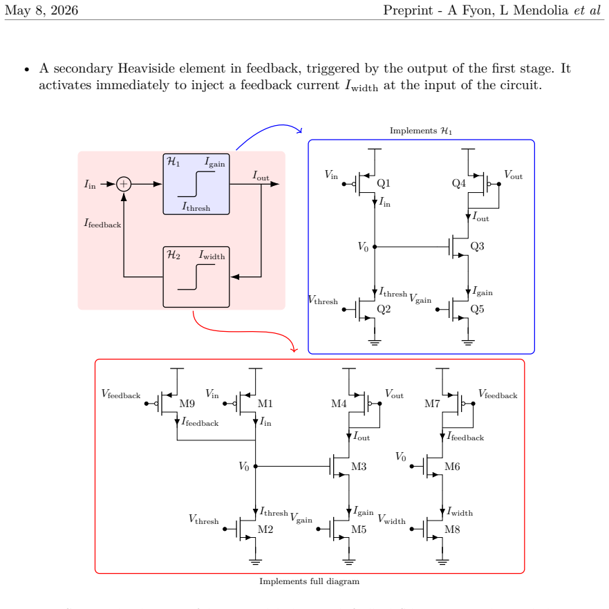
The central claim is that a unipolar memory cell built from nine standard MOSFET transistors can produce tunable bistable behavior entirely in the current domain. A new feedback arrangement between two thresholding elements allows the threshold current, the width of the hysteresis, and the output gain to be set independently. Simulations in a 180 nanometer process confirm that the cell maintains robust switching even when device parameters vary and that power stays in the nanowatt range with good temperature stability.
What carries the argument
The feedback configuration between two interdependent thresholding elements for producing tunable bistable switching
Load-bearing premise
Schematic simulations of the circuit in a 180 nanometer CMOS process will accurately reflect the performance of a real fabricated version, especially regarding hysteresis behavior, temperature stability, and tolerance to device mismatches.
What would settle it
Experimental results from a silicon prototype fabricated in 180 nanometer CMOS that measure the actual hysteresis width, power consumption under different temperatures, and consistency across multiple instances to check against the simulation predictions.
Figures


read the original abstract
This work introduces a fully tunable, ultra-low power unipolar memory cell inspired by the Schmitt-trigger comparator and designed in CMOS using only nine transistors. The proposed circuit operates entirely in the current domain and exploits a novel feedback configuration between two interdependent Heaviside-like thresholding elements to produce tunable bistable switching behavior. Its three key parameters-threshold current, hysteresis width, and output gain-are independently tunable via programmable bias currents, enabling flexibility across diverse analog computing applications. Unlike prior Schmitt-trigger designs, it simultaneously achieves current-mode operation, nanowatt-range power consumption, temperature stability, and full tunability, solely using standard MOSFET elements. Schematic-level simulations in a 180 nm CMOS process confirm robust hysteresis and resilience to device mismatch. Building on this circuit, we develop a complete family of spike-based logic gates using three-level current encoding, where the bistable memory retains the polarity of the last spike on each input indefinitely, enabling asynchronous logic operations without temporal windowing or refresh mechanisms. The same circuit also serves as the primitive for Bistable Memory Recurrent Units in analog neural networks, where the quantized hidden states provide inherent noise immunity. Together, these capabilities position the design as a versatile building block for next-generation neuromorphic processors integrating memory, logic, and recurrent computation.
Editorial analysis
A structured set of objections, weighed in public.
Referee Report
Summary. The manuscript introduces a nine-transistor current-mode unipolar memory cell in standard CMOS technology, inspired by the Schmitt-trigger comparator. It employs a novel feedback configuration between two interdependent Heaviside-like thresholding elements to achieve bistable switching, with independent tunability of threshold current, hysteresis width, and output gain via programmable bias currents. The design claims nanowatt-range power consumption, temperature stability, and resilience to device mismatch, supported by schematic-level simulations in a 180 nm CMOS process. Applications include spike-based logic gates using three-level current encoding and Bistable Memory Recurrent Units for analog neural networks.
Significance. If the performance claims hold under fabricated conditions, the circuit would provide a versatile, low-power tunable memory primitive suitable for neuromorphic processors, enabling asynchronous spike-based logic without temporal windowing or refresh and offering inherent noise immunity in recurrent neural units. The combination of current-mode operation, full independent tunability, and ultra-low power using only standard MOSFETs would distinguish it from prior Schmitt-trigger designs and support integration of memory, logic, and computation in analog systems.
major comments (2)
- [Abstract] Abstract: The statement that 'schematic-level simulations in a 180 nm CMOS process confirm robust hysteresis and resilience to device mismatch' lacks supporting evidence on the simulation setup. No indication is given of post-layout parasitic extraction, Monte Carlo analysis across process corners for mismatch, or temperature corner simulations, all of which are critical at nanowatt current levels where interconnect parasitics and well-proximity effects can alter feedback thresholds and degrade bistability.
- [Abstract] Abstract: The central claim that the nine-transistor cell 'simultaneously achieves current-mode operation, nanowatt-range power consumption, temperature stability, and full tunability' rests on the assumption that schematic simulations accurately predict fabricated behavior. Schematic-level analysis omits layout-dependent effects such as parasitic capacitances and local heating, which can shift effective switching thresholds and undermine the claimed temperature-stable Heaviside-like operation and mismatch resilience.
Simulated Author's Rebuttal
We thank the referee for the constructive feedback highlighting the need for clearer simulation details and more qualified claims in the abstract. We address each point below and will revise the manuscript accordingly.
read point-by-point responses
-
Referee: [Abstract] Abstract: The statement that 'schematic-level simulations in a 180 nm CMOS process confirm robust hysteresis and resilience to device mismatch' lacks supporting evidence on the simulation setup. No indication is given of post-layout parasitic extraction, Monte Carlo analysis across process corners for mismatch, or temperature corner simulations, all of which are critical at nanowatt current levels where interconnect parasitics and well-proximity effects can alter feedback thresholds and degrade bistability.
Authors: We agree that the abstract would benefit from additional context on the simulation methodology. In the revised manuscript we will expand the abstract and add a short simulation setup paragraph describing the use of the typical-typical corner in the 180 nm PDK, nominal 27 °C temperature, DC sweep and transient analyses with the listed bias currents, and targeted parameter sweeps to illustrate mismatch tolerance. We did not perform post-layout extraction, Monte Carlo statistical runs, or multi-corner temperature simulations because the work is presented at the schematic level to establish the circuit concept. We will explicitly qualify the abstract statement to read “schematic-level simulations … confirm …” and note the absence of layout-dependent effects as a limitation for future fabrication. revision: partial
-
Referee: [Abstract] Abstract: The central claim that the nine-transistor cell 'simultaneously achieves current-mode operation, nanowatt-range power consumption, temperature stability, and full tunability' rests on the assumption that schematic simulations accurately predict fabricated behavior. Schematic-level analysis omits layout-dependent effects such as parasitic capacitances and local heating, which can shift effective switching thresholds and undermine the claimed temperature-stable Heaviside-like operation and mismatch resilience.
Authors: The referee correctly notes that schematic results cannot fully capture layout parasitics or self-heating. We will revise the abstract to replace the unqualified claim with “schematic-level simulations indicate that the cell simultaneously achieves …” and will add a brief discussion paragraph acknowledging that interconnect capacitance and local heating may affect thresholds in a fabricated implementation. Temperature stability was verified only through schematic sweeps at 0 °C, 27 °C and 80 °C; we will report these specific conditions and state that full temperature-corner and post-layout validation remain future work. The core circuit topology and tunability results are unaffected by this clarification. revision: partial
Circularity Check
No significant circularity in circuit design or simulation-based claims
full rationale
The paper proposes an original nine-transistor current-mode Schmitt-trigger-inspired memory cell whose three tunable parameters are set directly by independent bias currents. All performance assertions (nanowatt power, temperature stability, mismatch resilience, bistable hysteresis) are supported by schematic-level simulations in 180 nm CMOS rather than by any closed mathematical derivation. No equations, fitted parameters renamed as predictions, self-definitional loops, or load-bearing self-citations appear in the provided text. The design choices and simulation results constitute independent content; the validation step does not reduce to the inputs by construction. This is the expected non-finding for a circuit-topology paper whose central claims rest on external simulation evidence.
Axiom & Free-Parameter Ledger
axioms (1)
- domain assumption Standard MOSFET models and simulation tools for 180 nm CMOS process accurately represent circuit behavior
Reference graph
Works this paper leans on
-
[1]
X. Ren et al. “A current-mode multiply-accumulate macro in sensing-computing fusion system for feature extraction and redundancy reduction”. In:IEEE Trans. Circuits Syst. II, Exp. Briefs(2025).doi:10.1109/tcsii.2025.3543173
-
[2]
Analog Versus Digital: Extrapolating from Electronics to Neurobiology
R. Sarpeshkar. “Analog Versus Digital: Extrapolating from Electronics to Neurobiology”. In: Neural Comput.10.7 (1998), pp. 1601–1638.doi:10.1162/089976698300017052
-
[3]
Memory devices and applications for in-memory computing
A. Sebastian et al. “Memory devices and applications for in-memory computing”. In:Nat. Nanotechnol.15.7 (2020), pp. 529–544.doi:10.1038/s41565-020-0655-z
-
[4]
In-Memory Computing with Resistive Switching Devices
D. Ielmini and H.-S. P. Wong. “In-Memory Computing with Resistive Switching Devices”. In: Nat. Electron.1.6 (2018), pp. 333–343.doi:10.1038/s41928-018-0092-2
-
[5]
Hardware implementation of memristor-based artificial neural networks
F. Aguirre et al. “Hardware implementation of memristor-based artificial neural networks”. In:Nat. Commun.15.1 (2024), p. 1974.doi:10.1038/s41467-024-45670-9
-
[6]
Challenges and trends of SRAM-based computing-in-memory for AI edge devices
C.-J. Jhang et al. “Challenges and trends of SRAM-based computing-in-memory for AI edge devices”. In:IEEE Trans. Circuits Syst. I68.5 (2021), pp. 1773–1786.doi: 10.1109/tcsi.2021.3064189
-
[7]
A review on SRAM-based computing in-memory: Circuits, functions, and applications
Z. Lin et al. “A review on SRAM-based computing in-memory: Circuits, functions, and applications”. In:J. Semicond.43.3 (2022), p. 031401.doi: 10.1088/1674-4926/43/3/031401
-
[8]
P. Mannocci et al. “A fully integrated analogue closed-loop in-memory computing accelerator based on static random-access memory”. In:Nat. Electron.(2026), pp. 1–13.doi: 10.1038/s41928-025-01549-1
-
[9]
H. Noguchi et al. “Which is the best dual-port SRAM in 45-nm process technology?—8T, 10T single end, and 10T differential”. In:2008 IEEE International Conference on Integrated Circuit Design and Technology and Tutorial. IEEE. 2008, pp. 55–58.doi: 10.1109/icicdt.2008.4567245
-
[10]
Physics for neuromorphic computing
D. Markovi´ c et al. “Physics for neuromorphic computing”. In:Nat. Rev. Phys.2.9 (2020), pp. 499–510.doi:10.1038/s42254-020-0208-2
-
[11]
Accurate deep neural network inference using computational phase-change memory
V. Joshi et al. “Accurate deep neural network inference using computational phase-change memory”. In:Nat. Commun.11.1 (2020), p. 2473.doi:10.1038/s41467-020-16108-9
-
[12]
Variability-aware memristive crossbars—a tutorial
A. P. James and L. O. Chua. “Variability-aware memristive crossbars—a tutorial”. In:IEEE Trans. Circuits Syst. II69.6 (2022), pp. 2570–2574.doi:10.1109/tcsii.2022.3169416
-
[13]
Research progress on solutions to the sneak path issue in memristor crossbar arrays
L. Shi et al. “Research progress on solutions to the sneak path issue in memristor crossbar arrays”. In:Nanoscale Adv.2.5 (2020), pp. 1811–1827.doi:10.1039/d0na00100g
-
[14]
A current-mode conductance-based silicon neuron for address-event neuromorphic systems
P. Livi and G. Indiveri. “A current-mode conductance-based silicon neuron for address-event neuromorphic systems”. In:Proc. IEEE Int. Symp. Circuits Syst. (ISCAS). 2009, pp. 2898–2901.doi:10.1109/iscas.2009.5118408. 9 May 8, 2026 Preprint - A Fyon, L Mendoliaet al
-
[15]
An ultra low power current-mode filter for neuromorphic systems and biomedical signal processing
C. Bartolozzi, S. Mitra, and G. Indiveri. “An ultra low power current-mode filter for neuromorphic systems and biomedical signal processing”. In:Proc. IEEE Biomed. Circuits Syst. Conf. (BioCAS). 2006, pp. 130–133.doi:10.1109/biocas.2006.4600325
-
[16]
2022 roadmap on neuromorphic computing and engineering
D. V. Christensen et al. “2022 roadmap on neuromorphic computing and engineering”. In: Neuromorphic Comput. Eng.2.2 (2022), p. 022501.doi:10.1088/2634-4386/ac4a83
-
[17]
L. Khacef et al. “Spike-based local synaptic plasticity: A survey of computational models and neuromorphic circuits”. In:Neuromorphic Comput. Eng.3.4 (2023), p. 042001.doi: 10.1088/2634-4386/ad05da
-
[18]
Opportunities for neuromorphic computing algorithms and applications
C. D. Schuman et al. “Opportunities for neuromorphic computing algorithms and applications”. In:Nat. Comput. Sci.2.1 (2022), pp. 10–19.doi: 10.1038/s43588-021-00184-y
-
[19]
A. Rubino et al.Neuromorphic analog circuits for robust on-chip always-on learning in spiking neural networks. 2023. arXiv:2307.06084 [cs.NE]
-
[20]
E. Gale. “Neuromorphic computation with spiking memristors: habituation, experimental instantiation of logic gates and a novel sequence-sensitive perceptron model”. In:Faraday Discuss.213 (2019), pp. 521–551.doi:10.1039/C8FD00111A
-
[21]
A. Ayuso-Martinez et al. “Construction of a spike-based memory using neural-like logic gates based on Spiking Neural Networks on SpiNNaker”. In:IEEE Trans. Emerg. Top. Comput.11 (2023), pp. 868–881.doi:10.1109/TETC.2023.3281063
-
[22]
LogicSNN: A Unified Spiking Neural Networks Logical Operation Paradigm
L. Mo and M. Wang. “LogicSNN: A Unified Spiking Neural Networks Logical Operation Paradigm”. In:Electronics10.17 (2021), p. 2123.doi:10.3390/electronics10172123
-
[23]
Logic gates based on neuristors made from two-dimensional materials
H. Chen et al. “Logic gates based on neuristors made from two-dimensional materials”. In: Nat. Electron.4.6 (2021), pp. 399–404.doi:10.1038/s41928-021-00591-z
-
[24]
Logic-in-memory based on an atomically thin semiconductor
G. Migliato Marega et al. “Logic-in-memory based on an atomically thin semiconductor”. In: Nature587.7832 (2020), pp. 72–77.doi:10.1038/s41586-020-2861-0
-
[25]
B. L. Doki´ c. “CMOS Schmitt triggers”. In:IEE Proc. G131 (1984), pp. 197–202.doi: 10.1049/ip-g-1.1984.0037
-
[26]
I. M. Filanovsky and H. Baltes. “CMOS Schmitt trigger design”. In:IEEE Trans. Circuits Syst. I41.1 (2002), pp. 46–49.doi:10.1109/81.260219
-
[27]
CMOS adjustable Schmitt triggers
Z. Wang. “CMOS adjustable Schmitt triggers”. In:IEEE Trans. Instrum. Meas.40.3 (2002), pp. 601–605.doi:10.1109/19.87026
-
[28]
A 160 mV robust Schmitt trigger based subthreshold SRAM
J. P. Kulkarni, K. Kim, and K. Roy. “A 160 mV robust Schmitt trigger based subthreshold SRAM”. In:IEEE J. Solid-State Circuits42.10 (2007), pp. 2303–2313.doi: 10.1109/jssc.2007.897148
-
[29]
Parallelizable memory recurrent units.arXiv preprint arXiv:2601.09495, 2026
F. De Geeter et al.Parallelizable memory recurrent units. 2026. arXiv:2601.09495 [cs.LG]
-
[30]
Brandoit et al.Combining Persistent Memory and Cumulative Update in Parallelizable RNNs
J. Brandoit et al.Combining Persistent Memory and Cumulative Update in Parallelizable RNNs. 2026. ORBi:2268/339664
work page 2026
-
[31]
Fyon et al.Co-Design of AI for Resource-Constrained Environments
A. Fyon et al.Co-Design of AI for Resource-Constrained Environments. 2026. ORBi: 2268/339660
work page 2026
-
[32]
M. Siripruchyanun and J. Hirunporm. “A fully/electronically controllable voltage-mode Schmitt trigger based on only single VDGA and its applications”. In:AEU - Int. J. Electron. Commun.131 (2021), p. 153602.doi:10.1016/j.aeue.2020.153602
-
[33]
M. Steyaert and W. Sansen. “Novel CMOS Schmitt trigger”. In:Electron. Lett.22.4 (1986), pp. 203–204.doi:10.1049/el:19860142
-
[34]
Novel approach to high-speed CMOS current comparators
H. Traff. “Novel approach to high-speed CMOS current comparators”. In:Electron. Lett.28.3 (1992), pp. 310–311.doi:10.1049/el:19920192
-
[35]
OTA-R Schmitt trigger with independently controllable threshold and output voltage levels
K. Kim, H.-W. Cha, and W.-S. Chung. “OTA-R Schmitt trigger with independently controllable threshold and output voltage levels”. In:Electron. Lett.33.13 (1997), pp. 1103–1105.doi:10.1049/el:19970786
-
[36]
Single CDBA-based voltage-mode bistable multivibrator and its applications
R. Pal et al. “Single CDBA-based voltage-mode bistable multivibrator and its applications”. In:Circuits Syst.6.11 (2015), pp. 237–251.doi:10.4236/cs.2015.611024
-
[37]
A novel current conveyor-based Schmitt trigger and its application as a relaxation oscillator
A. Srinivasulu. “A novel current conveyor-based Schmitt trigger and its application as a relaxation oscillator”. In:Int. J. Circuit Theory Appl.39.6 (2011), pp. 679–686.doi: 10.1002/cta.669. 10 May 8, 2026 Preprint - A Fyon, L Mendoliaet al
-
[38]
A simple fully controllable Schmitt trigger with electronic method using VDTA
M. Siripruchyanun, P. Satthaphol, and K. Payakkakul. “A simple fully controllable Schmitt trigger with electronic method using VDTA”. In:Appl. Mech. Mater.781 (2015), pp. 180–183.doi:10.4028/www.scientific.net/amm.781.180
-
[39]
Novel CMOS current Schmitt trigger
Z. Wang and W. Guggenbohl. “Novel CMOS current Schmitt trigger”. In:Electron. Lett. 24.24 (1988), pp. 1514–1516.doi:10.1049/el:19881034
-
[40]
F. Yuan. “A high-speed differential CMOS Schmitt trigger with regenerative current feedback and adjustable hysteresis”. In:Analog Integr. Circuits Signal Process.63.1 (2010), pp. 121–127.doi:10.1007/s10470-009-9374-y
-
[41]
Low-voltage subthreshold CMOS current mode circuits: Design and applications
M. A. Eldeeb et al. “Low-voltage subthreshold CMOS current mode circuits: Design and applications”. In:AEU-Int. J. Electron. Commun.82 (2017), pp. 251–264.doi: 10.1016/j.aeue.2017.08.049
-
[42]
A current-mode Schmitt trigger based on current differencing transconductance amplifier
T. Srivyshnavi and A. Srinivasulu. “A current-mode Schmitt trigger based on current differencing transconductance amplifier”. In:Proc. IEEE Int. Conf. Signal Process., Commun. Netw. (ICSCN). 2015, pp. 1–4.doi:10.1109/icscn.2015.7219884
-
[43]
Novel electronically controlled current-mode Schmitt trigger based on single active element
A. Kumar and B. Chaturvedi. “Novel electronically controlled current-mode Schmitt trigger based on single active element”. In:AEU - Int. J. Electron. Commun.82 (2017), pp. 160–166.doi:10.1016/j.aeue.2017.08.007
-
[44]
A simple current-mode Schmitt trigger employing only single MO-CTTA
P. Silapan and M. Siripruchyanun. “A simple current-mode Schmitt trigger employing only single MO-CTTA”. In:Proc. 6th IEEE Int. Conf. Electr. Eng./Electron., Comput., Telecommun. Inf. Technol. (ECTI-CON). 2009, pp. 556–559.doi: 10.1109/ecticon.2009.5137068
-
[45]
P. Silapan and M. Siripruchyanun. “Fully and electronically controllable current-mode Schmitt triggers employing only single MO-CCCDTA and their applications”. In:Analog Integr. Circuits Signal Process.68.1 (2011), pp. 111–128.doi:10.1007/s10470-010-9593-2
-
[46]
Current-mode Schmitt trigger based on ZC-current differencing transconductance amplifier
S. Madira, V. V. Reddy, and A. Srinivasulu. “Current-mode Schmitt trigger based on ZC-current differencing transconductance amplifier”. In:Proc. IEEE Int. Conf. Inventive Comput. Technol. (ICICT). 2016, pp. 1–5.doi:10.1109/inventive.2016.7823226
-
[47]
A Schmitt trigger based on DDCCTA without any passive components
R. Linitha, A. Srinivasulu, and V. V. Reddy. “A Schmitt trigger based on DDCCTA without any passive components”. In:Proc. IEEE Int. Conf. Commun. Signal Process. (ICCSP). 2015, pp. 1695–1698.doi:10.1109/iccsp.2015.7322808
- [48]
-
[49]
C. Banbury et al.MLPerf Tiny Benchmark. 2021. arXiv:2106.07597 [cs.LG]
-
[50]
MCUNet: Tiny Deep Learning on IoT Devices
J. Lin et al. “MCUNet: Tiny Deep Learning on IoT Devices”. In:Advances in Neural Information Processing Systems. Vol. 33. Virtual, 2020, pp. 11711–11722
work page 2020
-
[51]
Hello edge: Keyword spotting on microcontrollers,
Y. Zhang et al.Hello Edge: Keyword Spotting on Microcontrollers. 2017. arXiv:1711.07128 [cs.SD]. 11
discussion (0)
Sign in with ORCID, Apple, or X to comment. Anyone can read and Pith papers without signing in.