Recognition: no theorem link
Rashba engineering at van der Waals interfaces
Pith reviewed 2026-05-12 00:45 UTC · model grok-4.3
The pith
The interface between different TMD monolayers controls the sign and strength of Rashba spin splitting, enabling heterobilayers that outperform bulk materials in THz spintronic emission.
A machine-rendered reading of the paper's core claim, the machinery that carries it, and where it could break.
Core claim
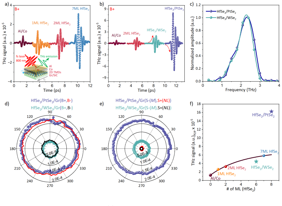
The interface between a large variety of two different epitaxially grown TMD monolayers controls the intensity and sign of the Rashba spin splitting, which is probed using THz spintronic emission. Optimized TMD heterobilayers, such as HfSe2/PtSe2, show enhanced THz emission that surpass the spin-to-charge conversion efficiency of bulk TMDs, confirming the presence of Rashba states with large spin splitting at the interface. By combining spin- and angle-resolved photoemission spectroscopy with density functional theory, we reveal that the electronic hybridization between the two different TMD monolayers gives rise to extended in-gap states with strong Rashba spin-orbit coupling. The choice of
What carries the argument
Electronic hybridization at the TMD heterobilayer van der Waals interface that generates extended in-gap states with large Rashba spin-orbit coupling.
Load-bearing premise
The enhanced THz emission and in-gap states are produced by interface hybridization and Rashba spin-orbit coupling rather than charge transfer, moiré patterns, or defects.
What would settle it
Quantitative agreement between the Rashba parameter measured by ARPES on the heterobilayer and the polarity plus amplitude of the THz emission signal predicted from the same band structure.
Figures


read the original abstract
Two-dimensional transition metal dichalcogenide (TMD) interfaces offer a versatile platform for studying emergent quantum phenomena and enabling novel device functionalities. When distinct TMD monolayers are stacked vertically or laterally stitched, their interfaces can exhibit unique electronic band alignments, giving rise to long-lived interlayer excitons, charge transfer effects, and moir\'e superlattices with correlated states. Here, we demonstrate that the interface between a large variety of two different epitaxially grown TMD monolayers controls the intensity and sign of the Rashba spin splitting, which is probed using THz spintronic emission. Optimized TMD heterobilayers, such as HfSe$_2$/PtSe$_2$, show enhanced THz emission that surpass the spin-to-charge conversion efficiency of bulk TMDs, confirming the presence of Rashba states with large spin splitting at the interface. By combining spin- and angle-resolved photoemission spectroscopy with density functional theory, we reveal that the electronic hybridization between the two different TMD monolayers gives rise to extended in-gap states with strong Rashba spin-orbit coupling. The choice of TMD layers enables to engineer the sign and strength of spin-to-charge conversion in van der Waals heterobilayers opening up perspectives to build efficient and tunable THz spintronic emitters.
Editorial analysis
A structured set of objections, weighed in public.
Referee Report
Summary. The manuscript investigates Rashba spin splitting at van der Waals interfaces of epitaxially grown TMD heterobilayers. It claims that stacking different TMD monolayers allows engineering of the sign and intensity of Rashba splitting, demonstrated by enhanced THz spintronic emission in heterobilayers such as HfSe2/PtSe2 that surpasses bulk TMD efficiency. This is attributed to electronic hybridization producing extended in-gap states with strong SOC, as revealed by SARPES and DFT calculations. The work positions these interfaces as tunable platforms for spin-to-charge conversion in THz emitters.
Significance. If substantiated, the results would provide a versatile route to engineer Rashba effects in 2D vdW systems beyond bulk materials, with direct implications for efficient, tunable THz spintronic devices. The multi-technique approach (THz emission, SARPES, DFT) and demonstration of layer-choice tunability are positive aspects that could advance the field of interface spintronics.
major comments (1)
- Abstract: The claim that enhanced THz emission in HfSe2/PtSe2 'surpass[es] the spin-to-charge conversion efficiency of bulk TMDs, confirming the presence of Rashba states with large spin splitting' is load-bearing but lacks a quantitative correlation. The Rashba parameter α_R extracted from SARPES and DFT must be directly compared to the inverse Rashba-Edelstein length inferred from the THz data; without this match and explicit single-layer controls, alternatives such as interfacial charge transfer, moiré potentials, or defects cannot be ruled out as the origin of the observed effects.
minor comments (2)
- Abstract: The phrasing 'a large variety of two different epitaxially grown TMD monolayers' is unclear and should be reworded for precision (e.g., 'various pairs of epitaxially grown TMD monolayers').
- Ensure all experimental figures (THz emission, SARPES) include error bars, sample statistics, and details on background subtraction to strengthen the 'enhanced' and 'surpass' claims.
Simulated Author's Rebuttal
We thank the referee for their positive evaluation of the significance of our work and for the detailed, constructive comment. We have carefully addressed the concern regarding the abstract claim and the need for quantitative correlation between techniques.
read point-by-point responses
-
Referee: Abstract: The claim that enhanced THz emission in HfSe2/PtSe2 'surpass[es] the spin-to-charge conversion efficiency of bulk TMDs, confirming the presence of Rashba states with large spin splitting' is load-bearing but lacks a quantitative correlation. The Rashba parameter α_R extracted from SARPES and DFT must be directly compared to the inverse Rashba-Edelstein length inferred from the THz data; without this match and explicit single-layer controls, alternatives such as interfacial charge transfer, moiré potentials, or defects cannot be ruled out as the origin of the observed effects.
Authors: We agree that a direct quantitative comparison would strengthen the manuscript. In the revised version we will extract the inverse Rashba-Edelstein length from the THz emission amplitudes and explicitly compare it to the α_R values obtained from SARPES and DFT for the same HfSe2/PtSe2 interface. We will also add a dedicated paragraph and supplementary figures comparing the heterobilayer results to single-layer TMD controls (where available from our growth and measurement campaigns) to help exclude charge-transfer or defect-dominated scenarios. While moiré potentials cannot be entirely excluded without additional microscopy, the observed sign reversal of the THz signal upon layer swapping and the appearance of extended in-gap states with strong SOC in our DFT calculations are signatures that are difficult to reconcile with moiré or simple charge-transfer pictures alone. We will tone down the abstract wording to reflect that the interface Rashba states are the most consistent explanation supported by the multi-technique data. revision: yes
Circularity Check
No significant circularity; claims rest on independent experiments and standard DFT
full rationale
The paper's derivation chain consists of experimental observations (THz spintronic emission exceeding bulk TMD controls, SARPES spectra) interpreted via standard DFT band-structure calculations showing hybridization-induced in-gap states. No load-bearing step reduces a prediction to a fitted input by construction, invokes a self-citation uniqueness theorem, or renames a known result as new unification. The sign and strength engineering is directly tied to measured emission polarity and DFT orbital character without self-referential definitions or ansatzes smuggled via prior work. This is the normal case of a self-contained experimental-computational study.
Axiom & Free-Parameter Ledger
axioms (1)
- standard math Standard density functional theory approximations for electronic structure calculations
Reference graph
Works this paper leans on
-
[1]
S. Manipatruni, D. E. Nikonov, C.-C. Lin, T. A. Gosavi, H. Liu, B. Prasad, Y.-L. Huang, E. Bonturim, R. Ramesh, and I. A. Young, Scalable energy-efficient magnetoelectric spin– orbit logic,Nature565, 35 (2019)
work page 2019
-
[2]
V. D. Nguyen, S. Rao, K. Wostyn, and S. Couet, Recent progress in spin-orbit torque magnetic random-access memory,npj Spintronics2, 48 (2024)
work page 2024
-
[3]
M. I. Dyakonov and V. I. Perel, Current-induced spin orientation of electrons in semiconduc- tors,Physics Letters A35, 459 (1971)
work page 1971
-
[4]
Yu. A. Bychkov and E. I. Rashba, Properties of 2D electron gas with lifted spectral degeneracy, JETP Letters39, 78 (1984)
work page 1984
-
[5]
K. Ando, S. Takahashi, J. Ieda, Y. Kajiwara, H. Nakayama, T. Yoshino, K. Harii, Y. Fujikawa, M. Matsuo, S. Maekawa, and E. Saitoh, Inverse spin-Hall effect induced by spin pumping in metallic system,Journal of Applied Physics109, 103913 (2011)
work page 2011
-
[6]
J. C. Rojas Sánchez, L. Vila, G. Desfonds, S. Gambarelli, J. P. Attáné, J. M. De Teresa, C. Magén, and A. Fert, Spin-to-charge conversion using Rashba coupling at the interface between non-magnetic materials,Nature Communications4, 2944 (2013)
work page 2013
-
[7]
T. Seifert, S. Jaiswal, U. Martens, J. Hannegan, L. Braun, P. Maldonado, F. Freimuth, A. Kronenberg, J. Henrizi, I. Radu, E. Beaurepaire, Y. Mokrousov, P. M. Oppeneer, M. Jour- dan, G. Jakob, D. Turchinovich, L. M. Hayden, M. Wolf, M. Münzenberg, M. Kläui, and T. Kampfrath, Efficient metallic spintronic emitters of ultrabroadband terahertz radiation, Natu...
work page 2016
-
[8]
M. B. Jungfleisch, Q. Zhang, W. Zhang, J. E. Pearson, R. D. Schaller, H. Wen, and A. Hoff- mann, Control of Terahertz Emission by Ultrafast Spin-Charge Current Conversion at Rashba Interfaces,Physical Review Letters120, 207207 (2018)
work page 2018
-
[9]
H. Yang, S. O. Valenzuela, M. Chshiev, S. Couet, B. Dieny, B. Dlubak, A. Fert, K. Garello, M. Jamet, D.-E. Jeong, K. Lee, T. Lee, M.-B. Martin, G. S. Kar, P. Sénéor, H.-J. Shin, and S. Roche, Two-dimensional materials prospects for non-volatile spintronic memories,Nature 606, 663 (2022)
work page 2022
-
[10]
R. Galceran, B. Tian, J. Li, F. Bonell, M. Jamet, C. Vergnaud, A. Marty, J. H. García, J. F. 19 Sierra, M. V. Costache, S. Roche, S. O. Valenzuela, A. Manchon, X. Zhang, and U. Schwingen- schlögl, Control of spin–charge conversion in van der Waals heterostructures,APL Materials 9, 100901 (2021)
work page 2021
-
[11]
K. Abdukayumov, M. Mičica, F. Ibrahim, L. Vojáček, C. Vergnaud, A. Marty, J.-Y. Veuillen, P. Mallet, I. G. de Moraes, D. Dosenovic, S. Gambarelli, V. Maurel, A. Wright, J. Tignon, J. Mangeney, A. Ouerghi, V. Renard, F. Mesple, J. Li, F. Bonell, H. Okuno, M. Chshiev, J.-M. George, H. Jaffrès, S. Dhillon, and M. Jamet, Atomic-Layer Controlled Transition fro...
work page 2024
-
[12]
K. Abdukayumov, O. Paull, M. Mičica, F. Ibrahim, L. Vojáček, A. Wright, S. Massabeau, F. Mazzola, V. Polewczyk, C. Jego, R. Sharma, C. Vergnaud, A. Marty, I. G. de Moraes, A. Ouerghi, H. Okuno, A. Jana, I. Kar, J. Fujii, I. Vobornik, L. M. Costa, O. Renault, J. Li, F.Bonell, M.Chshiev, M.Bibes, J.-M.George, H.Jaffrès, S.Dhillon, andM.Jamet, Monolayer Cont...
work page 2025
-
[13]
L. Cheng, X. Wang, W. Yang, J. Chai, M. Yang, M. Chen, Y. Wu, X. Chen, D. Chi, K. E. J. Goh, J.-X. Zhu, H. Sun, S. Wang, J. C. W. Song, M. Battiato, H. Yang, and E. E. M. Chia, Far out-of-equilibrium spin populations trigger giant spin injection into atomically thin MoS2, Nature Physics15, 347 (2019)
work page 2019
-
[14]
M. Mičica, A. Wright, S. Massabeau, S. Ayari, E. Rongione, M. O. Ribeiro, S. Husain, R. Sharma, T. Denneulin, R. E. Dunin-Borkowski, J. Mangeney, J. Tignon, R. Lebrun, H. Okuno, O. Boulle, A. Marty, F. Bonell, F. Carosella, H. Jaffrès, R. Ferreira, J.-M. George, M. Jamet, and S. Dhillon, Terahertz Electronic and Spin Currents in Wafer-Scale Van der Waals ...
work page 2026
-
[15]
S. Manzeli, D. Ovchinnikov, D. Pasquier, O. V. Yazyev, and A. Kis, 2D transition metal dichalcogenides,Nature Reviews Materials2, 17033 (2017)
work page 2017
-
[16]
S. Massabeau, O. Paull, A. Pezo, F. Miljevic, M. Mičica, A. Grisard, P. Morfin, R. Lebrun, H. Jaffrès, S. Dhillon, J.-M. George, M. Jamet, and M. Bibes, Inverse Rashba Edelstein THz emission modulation induced by ferroelectricity in CoFeB/PtSe2/MoSe2//LiNbO3 systems, APL Materials13, 041102 (2025)
work page 2025
-
[17]
M. T. Dau, M. Gay, D. Di Felice, C. Vergnaud, A. Marty, C. Beigné, G. Renaud, O. Renault, 20 P. Mallet, T. Le Quang, J.-Y. Veuillen, L. Huder, V. T. Renard, C. Chapelier, G. Zamborlini, M. Jugovac, V. Feyer, Y. J. Dappe, P. Pochet, and M. Jamet, Beyond van der Waals Inter- action: The Case of MoSe2 Epitaxially Grown on Few-Layer Graphene,ACS Nano12, 2319 (2018)
work page 2018
-
[18]
C. Vergnaud, M.-T. Dau, B. Grévin, C. Licitra, A. Marty, H. Okuno, and M. Jamet, New approach for the molecular beam epitaxy growth of scalable WSe2 monolayers,Nanotechnology 31, 255602 (2020)
work page 2020
-
[19]
E. Rongione, L. Baringthon, D. She, G. Patriarche, R. Lebrun, A. Lemaître, M. Morassi, N. Reyren, M. Mičica, J. Mangeney, J. Tignon, F. Bertran, S. Dhillon, P. Le Fèvre, H. Jaf- frès, and J.-M. George, Spin-Momentum Locking and Ultrafast Spin-Charge Conversion in Ultrathin Epitaxial Bi1−xSbx Topological Insulator,Advanced Science, 2301124 (2023)
work page 2023
-
[20]
L. Petersen and P. Hedegård, A simple tight-binding model of spin–orbit splitting of sp-derived surface states,Surface Science459, 49 (2000)
work page 2000
- [21]
-
[22]
E. E. Krasovskii, Microscopic origin of the relativistic splitting of surface states,Physical Review B90, 115434 (2014)
work page 2014
-
[23]
G. Manchon, S. Ghosh, C. Barreteau, and A. Manchon, Semirealistic tight-binding model for spin-orbit torques,Physical Review B101, 174423 (2020)
work page 2020
-
[24]
K. V. Shanavas, Z. S. Popović, and S. Satpathy, Theoretical model for Rashba spin-orbit interaction in d electrons,Physical Review B90, 165108 (2014)
work page 2014
-
[25]
T. Le Quang, V. Cherkez, K. Nogajewski, M. Potemski, M. T. Dau, M. Jamet, P. Mallet, and J.-Y. Veuillen, Scanning tunneling spectroscopy of van der Waals graphene/semiconductor interfaces: absence of Fermi level pinning,2D Materials4, 035019 (2017)
work page 2017
-
[26]
D. C. Vaz, P. Noël, A. Johansson, B. Göbel, F. Y. Bruno, G. Singh, S. McKeown-Walker, F. Trier, L. M. Vicente-Arche, A. Sander, S. Valencia, P. Bruneel, M. Vivek, M. Gabay, N. Bergeal, F. Baumberger, H. Okuno, A. Barthélémy, A. Fert, L. Vila, I. Mertig, J.-P. Attáné, and M. Bibes, Mapping spin–charge conversion to the band structure in a topological oxide...
work page 2019
-
[27]
A. Johansson, Theory of spin and orbital Edelstein effects,Journal of Physics: Condensed Matter36, 423002 (2024). 21
work page 2024
- [28]
-
[29]
L. Vojáček, J. Medina Dueñas, J. Li, F. Ibrahim, A. Manchon, S. Roche, M. Chshiev, and J. H. García, Field-Free Spin–Orbit Torque Switching in Janus Chromium Dichalcogenides, Nano Letters24, 11889 (2024)
work page 2024
-
[30]
S.S.Tsirkin, HighperformanceWannierinterpolationofBerrycurvatureandrelatedquantities with WannierBerri code,npj Computational Materials7, 33 (2021)
work page 2021
-
[31]
A. V. Krukau, O. A. Vydrov, A. F. Izmaylov, and G. E. Scuseria, Influence of the exchange screening parameter on the performance of screened hybrid functionals,The Journal of Chem- ical Physics125, 224106 (2006)
work page 2006
- [32]
-
[33]
C. Mastropasqua, A. El Alouani, M. Paillet, M. Portail, M. Koudia, M. Abel, Y. Cordier, B. Jouault, I. Berbezier, S. Juillaguet, and A. Michon, Self-limited monolayer graphene growth on SiC with propane-hydrogen CVD,npj 2D Materials and Applications9, 32 (2025)
work page 2025
-
[34]
P. E. Blöchl, Projector augmented-wave method,Physical Review B50, 17953 (1994)
work page 1994
-
[35]
G. Kresse and J. Hafner, Ab initio molecular dynamics for liquid metals,Physical Review B 47, 558 (1993)
work page 1993
-
[36]
G. Kresse and J. Furthmüller, Efficient iterative schemes for ab initio total-energy calculations using a plane-wave basis set,Physical Review B54, 11169 (1996)
work page 1996
-
[37]
G. Kresse and J. Furthmüller, Efficiency of ab-initio total energy calculations for metals and semiconductors using a plane-wave basis set,Computational Materials Science6, 15 (1996)
work page 1996
-
[38]
J. P. Perdew, K. Burke, and M. Ernzerhof, Generalized Gradient Approximation Made Simple, Physical Review Letters77, 3865 (1996)
work page 1996
- [39]
-
[40]
N. Marzari and D. Vanderbilt, Maximally localized generalized Wannier functions for compos- ite energy bands,Physical Review B56, 12847 (1997)
work page 1997
-
[41]
A. A. Mostofi, J. R. Yates, G. Pizzi, Y.-S. Lee, I. Souza, D. Vanderbilt, and N. Marzari, An 22 updated version of wannier90: A tool for obtaining maximally-localised Wannier functions, Computer Physics Communications185, 2309 (2014). 23
work page 2014
discussion (0)
Sign in with ORCID, Apple, or X to comment. Anyone can read and Pith papers without signing in.