Recognition: 2 theorem links
· Lean TheoremBand alignment of grafted diamond/GaN p-n heterojunctions interfaced with ALD Al2O3 and SiNx/Al2O3
Pith reviewed 2026-05-12 01:49 UTC · model grok-4.3
The pith
Inserting an SiNx layer increases band offsets by 0.42 eV in diamond/GaN heterojunctions with Al2O3.
A machine-rendered reading of the paper's core claim, the machinery that carries it, and where it could break.
Core claim
Both the diamond/Al2O3/GaN and diamond/Al2O3/SiNx/GaN structures exhibit type-II band alignment, but the band offsets in the version with the inserted SiNx layer are larger by 0.42 eV. This difference is attributed to a modification of the interfacial electrostatic potential, which may arise from a reduced density of positive fixed charges in the interfacial dielectric near the diamond/Al2O3 interface after insertion of the SiNx layer.
What carries the argument
X-ray photoelectron spectroscopy measurement of valence and conduction band offsets across the grafted interfaces, with SiNx insertion modifying the electrostatic potential in the ALD dielectric stack.
Load-bearing premise
The 0.42 eV difference in band offsets arises primarily from reduced positive fixed charge density near the diamond/Al2O3 interface due to SiNx insertion, rather than interface dipoles, defect states, or XPS artifacts.
What would settle it
Direct measurement of fixed charge density in the Al2O3 layer showing no reduction after SiNx addition, or finding identical band offsets in both structures.
Figures


read the original abstract
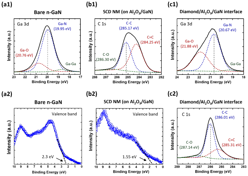
Diamond and gallium nitride are complementary semiconductors for forming p-n junctions because of their respective doping limitations. Understanding the band alignment of grafted diamond/GaN heterojunctions is therefore essential for optimizing diode performance. In this study, the band alignment of diamond/Al2O3/GaN and diamond/Al2O3/SiNx/GaN heterostructures was determined by X-ray photoelectron spectroscopy. Both structures exhibit type-II band alignment, but with different band offsets. The band offsets of the diamond/Al2O3/SiNx/GaN heterojunction are larger by 0.42 eV than those of diamond/Al2O3/GaN. This difference is attributed to a modification of the interfacial electrostatic potential, which may arise from a reduced density of positive fixed charges in the interfacial dielectric near the diamond/Al2O3 interface after insertion of the SiNx layer. These results demonstrate that interfacial-layer engineering provides an effective strategy for tailoring the band alignment of grafted diamond/GaN heterojunctions, offering guidance for the design of p-n diodes with tunable rectifying characteristics.
Editorial analysis
A structured set of objections, weighed in public.
Referee Report
Summary. The manuscript reports X-ray photoelectron spectroscopy (XPS) determination of band alignment in grafted diamond/Al2O3/GaN and diamond/Al2O3/SiNx/GaN heterostructures. Both exhibit type-II alignment, but the diamond/Al2O3/SiNx/GaN structure shows 0.42 eV larger valence- and conduction-band offsets. This difference is attributed to modification of the interfacial electrostatic potential, possibly from reduced positive fixed-charge density near the diamond/Al2O3 interface after SiNx insertion. The work concludes that interfacial-layer engineering can tailor band alignment for diamond/GaN p-n diodes.
Significance. If the measured offset difference is robust, the results provide concrete experimental values for band alignment in a technologically relevant wide-bandgap heterosystem where direct p-n formation is limited by doping constraints. The demonstration that an ALD SiNx interlayer can shift offsets by 0.42 eV offers a practical route for band-engineering in grafted junctions, with potential impact on diode rectification and carrier injection. The grafting-plus-ALD approach itself is device-relevant.
major comments (2)
- [Abstract and Discussion] Abstract and Discussion section: The attribution of the 0.42 eV offset increase to reduced positive fixed-charge density at the diamond/Al2O3 interface is presented as the primary explanation, yet remains inferential. No C-V, Kelvin-probe, or direct charge-density measurements are reported to isolate fixed charge from possible interface-dipole changes, defect-state shifts, or SiNx-induced chemical effects on XPS core-level referencing. This mechanism is load-bearing for the claim that interfacial engineering provides an 'effective strategy' for tunable rectifying characteristics.
- [Results and Experimental] Results and Experimental sections: The abstract and main text provide no quantitative error bars, standard deviations, or details on XPS peak-fitting procedures, inelastic mean-free-path assumptions, or controls for surface band bending and contamination. Without these, the statistical significance of the reported 0.42 eV difference cannot be assessed, undermining the central experimental claim.
minor comments (1)
- [Abstract] Abstract: The hedging phrase 'may arise' is appropriate, but the abstract would benefit from a clearer separation between the directly measured offsets and the proposed (unverified) mechanism.
Simulated Author's Rebuttal
We thank the referee for their constructive feedback and positive assessment of the significance of our XPS band-alignment measurements in grafted diamond/GaN heterostructures. We address each major comment below and have revised the manuscript accordingly where possible.
read point-by-point responses
-
Referee: [Abstract and Discussion] Abstract and Discussion section: The attribution of the 0.42 eV offset increase to reduced positive fixed-charge density at the diamond/Al2O3 interface is presented as the primary explanation, yet remains inferential. No C-V, Kelvin-probe, or direct charge-density measurements are reported to isolate fixed charge from possible interface-dipole changes, defect-state shifts, or SiNx-induced chemical effects on XPS core-level referencing. This mechanism is load-bearing for the claim that interfacial engineering provides an 'effective strategy' for tunable rectifying characteristics.
Authors: We agree that the proposed mechanism remains inferential, as the manuscript does not include direct measurements of fixed charge (C-V or Kelvin probe). The original text already employs cautious phrasing ('may arise from'), but we accept that the discussion could more explicitly acknowledge alternative contributions such as interface dipoles or SiNx-induced chemical shifts. In the revised manuscript we will expand the Discussion section to list these alternatives, moderate the abstract and conclusion to emphasize the experimentally observed 0.42 eV offset increase rather than the specific charge-density hypothesis, and retain the claim that interfacial-layer engineering is effective on the basis of the measured shift itself. We do not possess C-V or Kelvin-probe data for this study. revision: partial
-
Referee: [Results and Experimental] Results and Experimental sections: The abstract and main text provide no quantitative error bars, standard deviations, or details on XPS peak-fitting procedures, inelastic mean-free-path assumptions, or controls for surface band bending and contamination. Without these, the statistical significance of the reported 0.42 eV difference cannot be assessed, undermining the central experimental claim.
Authors: We acknowledge this omission. The revised manuscript will include quantitative error bars on all reported band-offset values (derived from XPS peak-fitting uncertainties and replicate measurements), standard deviations where multiple samples were measured, and expanded Experimental-section details on peak-fitting routines, inelastic-mean-free-path values and sources, and procedures used to minimize or correct for surface band bending and adventitious contamination. These additions will enable readers to evaluate the significance of the 0.42 eV difference. revision: yes
Circularity Check
No circularity: experimental XPS band-offset measurements with inferential attribution only
full rationale
The manuscript is a pure experimental study reporting X-ray photoelectron spectroscopy (XPS) core-level shifts to extract valence-band offsets for diamond/Al2O3/GaN and diamond/Al2O3/SiNx/GaN stacks. The 0.42 eV difference is stated as an observation and then attributed (with hedging language 'may arise') to possible fixed-charge modification; no equations, fitted parameters, predictions, or derivations are presented. No self-citations are invoked to justify uniqueness theorems or ansatzes. The result is therefore self-contained against external benchmarks (XPS data) and receives the default non-circularity score.
Axiom & Free-Parameter Ledger
axioms (1)
- domain assumption XPS measurements accurately reflect bulk band offsets at the buried interfaces after accounting for surface effects
Lean theorems connected to this paper
-
IndisputableMonolith/Cost/FunctionalEquation.leanwashburn_uniqueness_aczel unclearThe band offsets of the diamond/Al2O3/SiNx/GaN heterojunction are larger by 0.42 eV than those of diamond/Al2O3/GaN. This difference is attributed to a modification of the interfacial electrostatic potential, which may arise from a reduced density of positive fixed charges...
-
IndisputableMonolith/Foundation/AbsoluteFloorClosure.leanreality_from_one_distinction unclearUsing the Kraut method... VBO ... 0.63 eV ... CBO ... 2.70 eV
Reference graph
Works this paper leans on
-
[1]
1 W. A. Doolittle, C. M. Matthews, H. Ahmad, K. Motoki, S. Lee, A. Ghosh, and P. D. Yoder, “Prospectives for AlN electronics and optoelectronics and the important role of alternative synthesis,” Appl. Phys. Lett. 123, 070501 (2023). 2 S. J. Pearton, F. Ren, M. Tadjer, and J. Kim, “Perspective: Ga₂O₃ for ultra -high power rectifiers and MOSFETs,” J. Appl. ...
work page 2023
-
[2]
Characteristics of native oxides-interfaced GaAs/Ge np diodes,
Wang, F. Xia, and Z. Ma, “Characteristics of native oxides-interfaced GaAs/Ge np diodes,” IEEE Electron Device Lett. 45, 1669 (2024). 19 J. Zhou, H. Wang, P.R. Huang, S. Xu, Y. Liu, J. Gong, J. Shen, D. Vicent, S. Haessly, A. Abrand, P.K. Mohseni, M. Kim, S.- Q. Yu, G. -E. Chang, X. Gong, and Z. Ma, “GaAs/GeSn/Ge n–i –p diodes and light emitting diodes fo...
work page 2024
-
[3]
Lattice -mismatched semiconductor heterostructures,
Baboli, J. Park, J. Bong, I.-K. Lee, J. Gong, S. Mikael, J. H. Ryu, P. K. Mohseni, X. Li, S. Gong, X. Wang, and Z. Ma, “Lattice -mismatched semiconductor heterostructures,” arXiv:1812.10225 (2018). 21 J. Gong, D. Kim, H. Jang, F. Alema, Q. Wang, J. Zhou, Y. Li, T.K. Ng, S. Qiu, Y. Liu, M
-
[4]
Characteristics of grafted monocrystalline Si/β-Ga2O3 p–n heterojunction,
Sheikhi, Y. Lu, R. Singh, X. Su, H.N. Abbasi, Q. Lin, S. Xie, K. Chabak, G. Jessen, C. Cheung, V. Gambin, S.S. Pasayat, A. Osinsky, B.S. Ooi, C. Gupta, and Z. Ma, “Characteristics of grafted monocrystalline Si/β-Ga2O3 p–n heterojunction,” Appl. Phys. Lett. 124, 262101 (2024). 22 J. Gong, J. Zhou, A. Dheenan, M. Sheikhi, F. Alema, T. K. Ng, S. S. Pasayat, ...
-
[5]
Liu, Z. Liu, M. Nong, K. Fountaine, V. Gambin, X. Li, and Z. Ma, “Band alignment and leakage mechanism analysis of p -Si/n-AlN heterojunction diodes with the Al ₂O₃ interlayer,” ACS Appl. Electron. Mater. 7, 9700–9709 (2025). 29 J. Zhou, H. Wang, Y. Guo, A. Abrand, Y. Li, Y. Liu, J. Gong, P.R. Huang, J. Shen, and S. Xu, “Optoelectronically Active GaAs/GeS...
-
[6]
Lu, T. - H. Tsai, Y. Li, V. Gambin, T. K. Ng, B. S. Ooi, and Z. Ma, “Grafted GaAs/Si Heterojunction Tunnel Diodes with Improved Peak- to-valley Current Ratio (PVCR) of up to 36.38,” IEEE Electron Device Lett. 1–1 (2025). 31 J. Zhou, Y. Lu, C. Wang, L. Suter, A. Hardy, T. K. Ng, K. Sun, Y. Guo, Y. Liu, T. -H. Tsai, X
work page 2025
-
[7]
Preliminary demonstration of diamond– GaN p–n diodes via grafting,
Zhou, C. S. Bailey, M. Eller, S. Liu, Z. Mi, B. S. Ooi, M. Muehle, K. Fountaine, V. Gambin, J.-H. Seo, and Z. Ma, “Preliminary demonstration of diamond– GaN p–n diodes via grafting,” arXiv 2510.25028 (2025). 32 E. A. Kraut, R. W. Grant, J. R. Waldrop, and S. P. Kowalczyk, “Precise determination of the valence-band edge in x-ray photoemission spectra: Appl...
-
[8]
Low -temperature processing to obtain cont act resistance of <0.03 Ohm mm to boron-doped diamond,
Myszka, M. A. Hollis, T. G. Ivanov, A. G. Birdwell, D. Ruzmetov, J. Weil, N. R. Jankowski, T. A. Grotjohn, and B. Zhang, “Low -temperature processing to obtain cont act resistance of <0.03 Ohm mm to boron-doped diamond,” Phys. Status Solidi A 222, 2400636 (2025). 36 A. Hardy, M. Muehle, C. Herrera-Rodriguez, M. Becker, E. Drown, N. Baule, M. Tompkins, T. ...
work page 2025
-
[9]
Liu, D. Liu, S. Qiu, B. S. Ooi, I. Roqan, and Z. Ma, “Investigation of ultrathin surface passivation layers for GaN: a comparative analysis of Al₂O₃, SiO₂, and SiNₓ in reducing surface recombination,” Appl. Phys. Lett. 127, 011601 (2025). 50 Z. Yatabe, J. Asubar, and T. Hashizume, “Insulated gate and surface passivation structures for GaN-based power tran...
work page 2025
discussion (0)
Sign in with ORCID, Apple, or X to comment. Anyone can read and Pith papers without signing in.