Recognition: no theorem link
TPA-TCT Analysis of the RD50-MPW4 Monolithic Pixel Particle Detector
Pith reviewed 2026-05-13 04:54 UTC · model grok-4.3
The pith
The RD50-MPW4 monolithic pixel detector collects 100% of generated charge across a 226 micrometer depletion depth.
A machine-rendered reading of the paper's core claim, the machinery that carries it, and where it could break.
Core claim
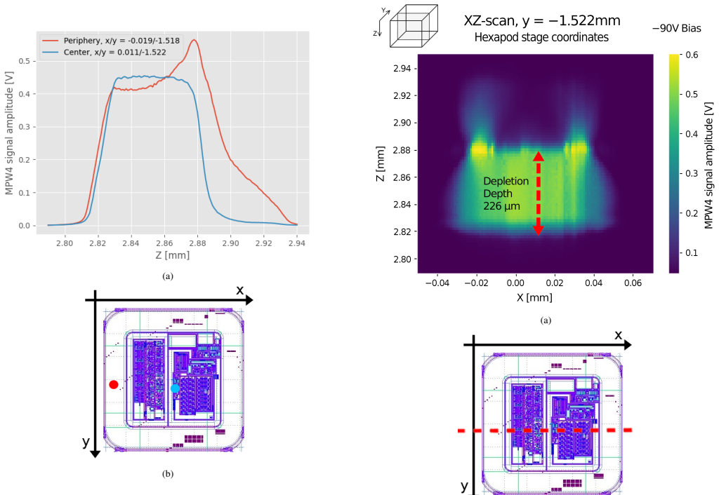
Using TPA-TCT with backside illumination at 1550 nm, the RD50-MPW4 sensor exhibits 100% charge collection efficiency and a depletion depth of 226 micrometers. Three-dimensional maps show the boundaries of the sensitive volume and partial charge collection from the pixel periphery into neighboring pixels.
What carries the argument
The TPA-TCT technique, which generates electron-hole pairs only at the laser focal point deep in the silicon due to two-photon absorption, enabling precise spatial mapping of charge collection.
If this is right
- The full efficiency supports deployment of this pixel matrix in tracking detectors without loss of signal.
- Charge sharing at pixel boundaries must be included in algorithms that reconstruct hit positions.
- The measured 226 micrometer depletion depth defines the active thickness available for particle ionization.
- In-pixel electronics create visible boundaries in the electric field that limit the sensitive volume.
Where Pith is reading between the lines
- The same backside-illumination approach could map depletion regions in other HV-CMOS designs without altering the chip.
- Significant peripheral charge sharing may limit the ultimate spatial resolution in high-density particle environments.
- Confirmation of uniform efficiency across the 62 by 62 micrometer pixels reduces the need for per-pixel calibration in large arrays.
Load-bearing premise
Charge carriers produced by two-photon absorption at the laser focus behave identically to those from minimum-ionizing particles, with no significant differences in track structure or recombination.
What would settle it
A side-by-side efficiency and depth measurement on the same RD50-MPW4 sensor using a real minimum-ionizing particle beam versus the TPA-TCT laser setup.
Figures


read the original abstract
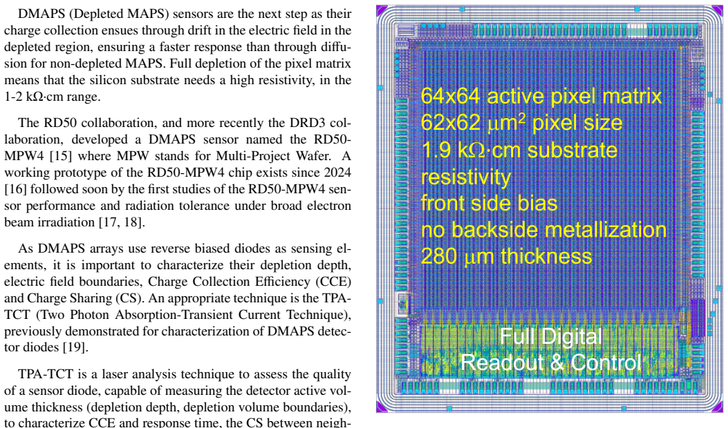
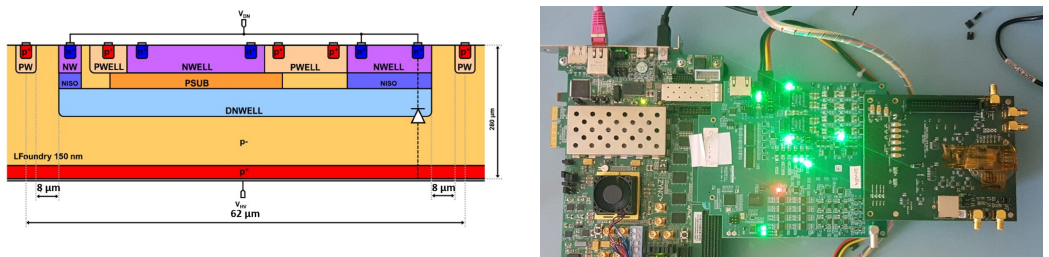
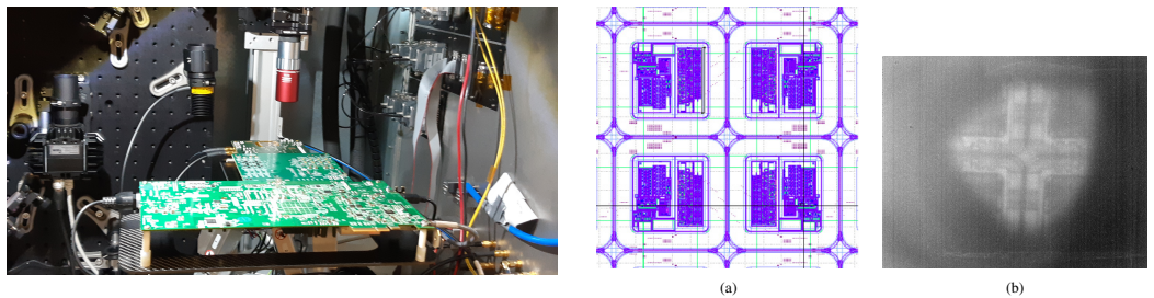
The RD50-MPW4, a Depleted Monolithic Active Pixel Sensor (DMAPS) was analyzed using a Two Photon Absortion Transient Current Technique (TPA-TCT). This technique provides sensitivity maps with micrometer-scale spatial resolution, enabling the resolution of the boundaries of the detector's sensitive volume, even for small-area pixels (62x62 squared micrometers in this study). With a full 3D resolution, the depletion depth, the boundaries of the detector electric field, the 3D hit detection efficiency and the charge sharing between neighboring pixels were measured. The RD50-MPW4, a multi-project wafer chip developed by the HV-CMOS working group within the CERN RD50 collaboration, features a 64x64 DMAPS pixel matrix. Illuminating the chip from the backside, the TPA-TCT technique can characterize any pixel element in the matrix because silicon is transparent for near infrared laser light (1550 nm). Electron-hole pairs are generated only around the light focal point, deep in the silicon, so that any charge collected is precisely only from the focal point. With the TPA-TCT technique, the RD50-MPW4 was found to be have a 100\% charge collection efficiency and a depletion depth of 226 $\upmu$m. It was also found that part of the charge in the periphery of the pixel was collected in the neighboring pixel. A 3D map of the sensor clearly shows the in-pixel electronics and the limits of the depletion region.
Editorial analysis
A structured set of objections, weighed in public.
Referee Report
Summary. The manuscript reports on the characterization of the RD50-MPW4 depleted monolithic active pixel sensor (DMAPS) using the two-photon absorption transient current technique (TPA-TCT). It claims a 100% charge collection efficiency, a depletion depth of 226 μm, observation of charge sharing between neighboring pixels, and 3D sensitivity maps that resolve the boundaries of the sensitive volume, electric field limits, and in-pixel electronics for the 62×62 μm² pixels, obtained by backside illumination with a 1550 nm laser.
Significance. If validated, the TPA-TCT results provide high-resolution 3D mapping of charge collection and depletion in a small-pixel DMAPS, which is valuable for optimizing monolithic sensors in particle physics applications. The technique's ability to isolate charge generation at a focal point offers complementary data to beam tests, but its direct applicability to MIP performance requires explicit justification.
major comments (2)
- [Abstract and results] Abstract and results: The claims of 100% charge collection efficiency and 226 μm depletion depth are derived from integrated TPA-TCT signals, but the manuscript provides no direct cross-validation (e.g., beam-test comparison or TCAD simulation) quantifying how the localized Gaussian charge packet (~few μm) from two-photon absorption differs from the extended uniform ionization track of MIPs in terms of recombination, trapping, or lateral diffusion under the same bias conditions. This assumption is load-bearing for interpreting the numbers as particle-detector metrics rather than laser-specific responses.
- [Abstract] Abstract: The reported depletion depth of 226 μm and 100% efficiency are stated without accompanying uncertainties, details on the charge-integration threshold used to define the boundary, or calibration of the TPA-TCT signal amplitude against known charge deposits, which weakens the quantitative strength of the central claims.
minor comments (3)
- [Abstract] Abstract: Typo in 'was found to be have a 100%'; should read 'was found to have a 100%'.
- [Abstract] Abstract: 'squared micrometers' should be 'μm²' for consistency with standard notation; the pixel size is given as '62x62 squared micrometers'.
- [Results] The manuscript would benefit from a brief discussion of how the 3D hit detection efficiency is extracted from the TPA-TCT maps and whether any position-dependent weighting or threshold is applied.
Simulated Author's Rebuttal
We thank the referee for the careful and constructive review of our manuscript. We address each major comment below, providing clarifications on the TPA-TCT methodology and its interpretation for the RD50-MPW4 sensor.
read point-by-point responses
-
Referee: [Abstract and results] Abstract and results: The claims of 100% charge collection efficiency and 226 μm depletion depth are derived from integrated TPA-TCT signals, but the manuscript provides no direct cross-validation (e.g., beam-test comparison or TCAD simulation) quantifying how the localized Gaussian charge packet (~few μm) from two-photon absorption differs from the extended uniform ionization track of MIPs in terms of recombination, trapping, or lateral diffusion under the same bias conditions. This assumption is load-bearing for interpreting the numbers as particle-detector metrics rather than laser-specific responses.
Authors: We agree that the localized charge generation in TPA-TCT (a few-micrometer Gaussian packet) differs from the extended MIP track, and this distinction merits explicit discussion. The 100% CCE reported here reflects full collection of charge generated at the focal point when scanned throughout the depleted volume, indicating negligible recombination or trapping within the high-field region under the applied bias. The depletion depth is extracted from the z-position at which collected charge falls to the noise floor. While this work focuses on the 3D mapping capability of TPA-TCT rather than direct MIP equivalence, the technique has been cross-validated against beam tests in prior RD50 studies on similar HV-CMOS devices. We will add a dedicated paragraph in the revised manuscript discussing the charge-density differences, expected lateral diffusion, and why the measured CCE and depth remain representative metrics for the sensor's sensitive volume in particle-physics applications. revision: partial
-
Referee: [Abstract] Abstract: The reported depletion depth of 226 μm and 100% efficiency are stated without accompanying uncertainties, details on the charge-integration threshold used to define the boundary, or calibration of the TPA-TCT signal amplitude against known charge deposits, which weakens the quantitative strength of the central claims.
Authors: We accept this criticism. The depletion depth was obtained by stepping the focal point in 2 μm increments along z and identifying the boundary where the integrated current signal drops below a 3σ noise threshold; the 100% efficiency is normalized to the maximum signal observed at the pixel center. The TPA-TCT amplitude was calibrated using the known two-photon absorption cross-section and laser pulse energy, referenced to prior characterizations of similar sensors. In the revised version we will report the uncertainty (±4 μm) derived from scan step size and signal-to-noise ratio, explicitly state the integration window and threshold criterion, and include a brief calibration description with a reference to the established TPA-TCT charge-scale method. revision: yes
Circularity Check
No significant circularity: purely experimental measurements
full rationale
The paper reports direct experimental results obtained via TPA-TCT laser scanning of the RD50-MPW4 sensor, including measured charge collection efficiency of 100%, depletion depth of 226 μm, and observed charge sharing in pixel peripheries. These quantities are extracted from integrated signal maps versus position and depth with no mathematical derivations, no parameters fitted to a subset of data and then presented as predictions, and no load-bearing self-citations or uniqueness theorems. The analysis consists of independent physical measurements of observed signals and is therefore self-contained against external benchmarks.
Axiom & Free-Parameter Ledger
axioms (2)
- domain assumption Silicon is transparent at 1550 nm wavelength allowing backside illumination
- domain assumption Electron-hole pairs are generated only at the two-photon absorption focal point
Reference graph
Works this paper leans on
-
[1]
N. Wermes,Pixel detectors ... where do we stand?, Nuclear Instruments and Methods in Physics Research Section A vol. 924, pp. 44-50, Apr. 2019, DOI: 10.1016/j.nima.2018.07.003
-
[2]
B. Kamtchou et al.,An experimental and computational evaluation of a novel Timepix3 detector for Compton imaging in nuclear medicine, Journal of Instrumenta- tion, vol. 19, no. 12, pp. P12004, Dec. 2024, DOI: 10.1088/1748-0221/19/12/P12004
-
[3]
A. L. Steinhebel et al.,AstroPix: A pixelated HVC- MOS sensor for space-based gamma-ray measurement, Nuclear Instruments and Methods in Physics Research Section A, vol. 1083, pp. 171021, Mar. 2026, DOI: 10.1016/j.nima.2025.171021
-
[4]
Y . Kim et al.,Radiation measurement and imaging using 3D position sensitive pixelated CZT detector, Nuclear En- gineering and Technology, vol. 51, no. 5, pp. 1417-1427, Aug. 2019, DOI: 10.1016/j.net.2019.03.009
-
[6]
F. Hartmann,Evolution of Silicon Sensor Technology in Particle Physics: Basics and Applications, Springer, 2024, DOI: 10.1007/978-3-031-59720-6
-
[7]
The RD53 Collaboration et al.,RD53 pixel readout inte- grated circuits for ATLAS and HL-LHC upgrades, Journal of Instrumentation, vol. 20, no. 3, pp. P03024, Mar. 2025, DOI: 10.1088/1748-0221/20/03/P03024
-
[8]
W. Snoeys,Monolithic CMOS sensors for high en- ergy physics - Challenges and perspectives, Nuclear Instruments and Methods in Physics Research Sec- tion A, vol. 1056, pp. 168678, Nov. 2023, DOI: 10.1016/j.nima.2023.168678
-
[9]
G. Contin et al.,The STAR MAPS-based PiXeL detec- tor, Nuclear Instruments and Methods in Physics Re- search Section A, vol. 907, pp. 60-80, Nov. 2018, DOI: 10.1016/j.nima.2018.03.003. 8
-
[11]
G.A. Rinella on behalf of the ALICE collaboration,The ALPIDE sensor chip for the upgrade of the ALICE In- ner Tracking System, Nuclear Instruments and Methods in Physics Research A, vol. 845, pp.583-587, Feb. 2014, DOI: 10.1016/j.nima.2016.05.016
-
[12]
N. Valle and ALICE Collaboration,Performance of the ALICE Inner Tracking System 2, Nuclear Instruments and Methods in Physics Research A, vol. 1079, pp. 170596, Oct. 2025, DOI:10.1016/j.nima.2025.170596
-
[13]
ALICE Collaboration,Technical design report for the upgrade of the ALICE Inner Tracking System, Jour- nal of Physics G: Nuclear and Particle Physics, vol. 41, no. 8, pp. 087002, Jul. 2014, DOI: 10.1088/0954- 3899/41/8/087002
-
[15]
E. Vilella on behalf of the CERN-RD50 collabora- tion,Development of high voltage-CMOS sensors within the CERN-RD50 collaboration, Nuclear Instruments and Methods in Physics Research Section A, vol. 1034, pp. 166826, Jul. 2022, DOI: 10.1016/j.nima.2022.166826
-
[16]
E.Vilella et al.,RD50-MPW4: a thin backside- biased High Voltage CMOS pixel chip for high ra- diation tolerance, Journal of Instrumentation, vol. 20, no. 3, pp. C03044, Mar. 2025, DOI: 10.1088/1748- 0221/20/03/C03044
-
[17]
2024, DOI: 10.1016/j.nima.2024.169839
B.Pilsl a et al.,Characterization of the RD50-MPW4 HV- CMOS pixel sensor, Nuclear Instruments and Methods in Physics Research A, vol.1069, pp.169839, Dec. 2024, DOI: 10.1016/j.nima.2024.169839
-
[18]
2025, DOI: 10.1016/j.nima.2025.170752
B.Pilsl a et al.,Enhancing radiation hardness and granularity in HV-CMOS: The RD50-MPW4 sensor, Nuclear Instruments and Methods in Physics Re- search A, vol.1080, pp.170752, Nov. 2025, DOI: 10.1016/j.nima.2025.170752
-
[19]
F.Palomo et al.,Characterization of the RD50-MPW2 monolithic CMOS sensor with the TPA-TCT technique, IEEE Sensors Journal, vol. 25, no. 18, pp. 34575-34582, Sep. 2025, DOI: 10.1109/JSEN.2025.3592456
-
[20]
K. S. Shah et al.,Charge collection efficiency in a semi- conductor radiation detector with a non-constant electric field, IEEE Transactions on Nuclear Science, vol. 37, no. 2, pp. 183-186, Apr. 1990, DOI: 10.1109/23.106615
-
[21]
K. Ramaswami et al.,Charge collection efficiency in pho- toconductive detectors under small to large signals, Jour- nal of Applied Physics, vol. 125, no. 24, p. 244503, Jun. 2019, DOI: 10.1063/1.5096900
-
[22]
I. Mandi ´c et al.,Study of neutron irradiation effects in Depleted CMOS detector structures, Journal of Instru- mentation, vol. 17, no. 3, pp. P03030, Mar. 2022, DOI: 10.1088/1748-0221/17/03/p03030
-
[23]
Y . Otarid et al.,A versatile data acquisition system for silicon pixel detector prototyping, Journal of Instrumen- tation, vol. 20, no. 7, pp. C07043, Jul. 2025, DOI: 10.1088/1748-0221/20/07/C07043
-
[24]
Peary Software,Peary DAQ (Caribou Project),https: //caribou-project.docs.cern.ch/, 2025
work page 2025
-
[25]
M. Wiehe et al.,Development of a Tabletop Setup for the Transient Current Technique Using Two-Photon Absorp- tion in Silicon Particle Detectors, IEEE Transactions on Nuclear Science, vol. 68, no. 2, pp. 220-228, Feb. 2021, DOI: 10.1109/TNS.2020.3044489
-
[26]
A. Almagro et al.,Fiber laser system of 1550 nm fem- tosecond pulses with configurable properties for the two- photon excitation of transient currents in semiconductor detectors, Applied Optics, vol. 61, no. 32, pp. 9386-9397, Nov. 2022, DOI: 10.1364/AO.470780
-
[27]
F. R. Palomo et al.,Plasma effects in silicon detectors and the two photon absorption transient current technique, 2021 21th European Conference on Radiation and Its Ef- fects on Components and Systems (RADECS), pp. 1-6, 2021, DOI: 10.1109/RADECS53308.2021.9954488
-
[28]
S. Pape,Characterisation of Silicon Detectors Using the Two Photon Absorption - Transient Current Technique, Ph.D. dissertation, Tech. U. Dortmund, Dortmund, Ger- many, 2023. 9
work page 2023
discussion (0)
Sign in with ORCID, Apple, or X to comment. Anyone can read and Pith papers without signing in.