Recognition: no theorem link
Engineering few-layer graphene by S-doping: from sustaining linear dispersion to flat bands
Pith reviewed 2026-05-13 04:22 UTC · model grok-4.3
The pith
Sulfur doping in few-layer graphene can sustain linear dispersion, open gaps, or create flat bands near the Fermi level depending on configuration and layer count.
A machine-rendered reading of the paper's core claim, the machinery that carries it, and where it could break.
Core claim
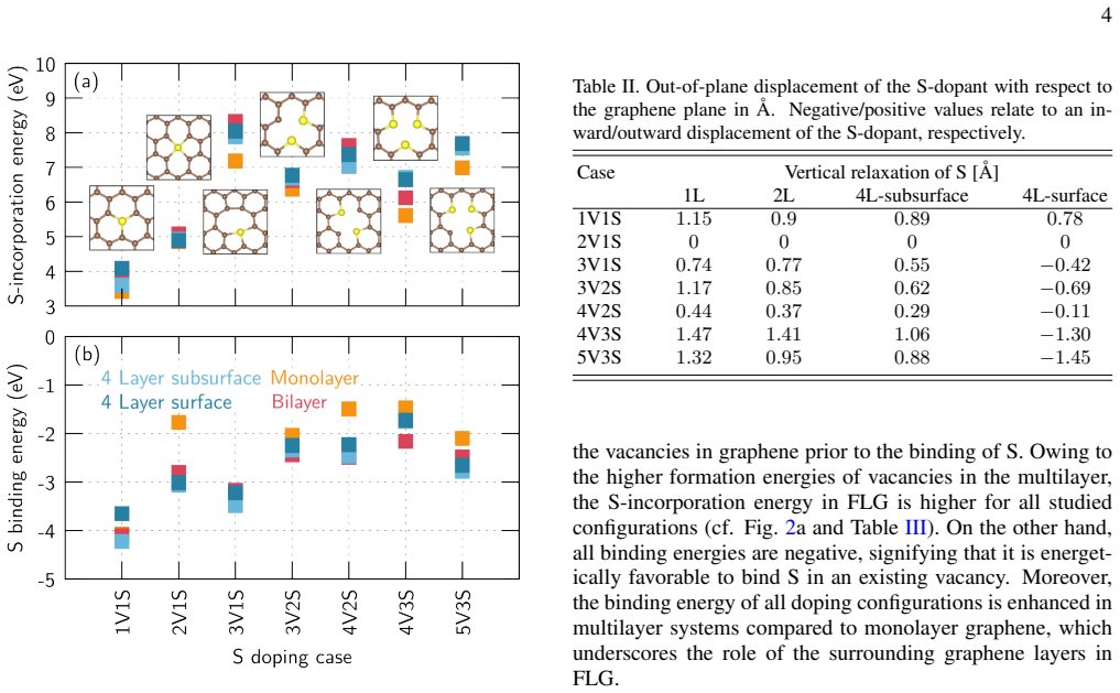
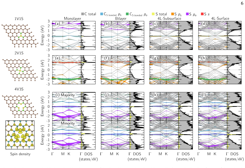
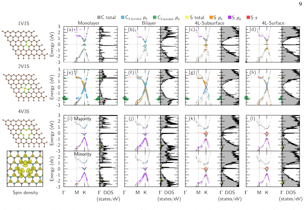
In monolayer graphene, thiophenic doping (2V1S) sustains the Dirac cone with localized impurity bands, graphitic doping (1V1S) opens a 0.4 eV gap with flat bands near the Fermi level, and 4V3S adds n-type doping plus spin polarization. When the same motifs are placed in bi- and four-layer systems the Dirac cone turns into hyperbolic touching bands, gaps are reduced or closed, flat bands appear at the Fermi level, and spin polarization weakens, allowing the electronic behavior of few-layer graphene to be tuned from metallic to insulating and from linear dispersive to flat bands.
What carries the argument
Basal-plane sulfur doping configurations (2V1S thiophenic, 1V1S graphitic, 4V3S with three S atoms in a four-site vacancy) that modify the band dispersion and Fermi-level states through first-principles DFT calculations with van der Waals corrections in one- to four-layer systems.
If this is right
- Choice of S-doping motif and number of layers can switch few-layer graphene between metallic and insulating states.
- The band structure can be shifted from linear dispersive cones to flat bands close to the Fermi level.
- S-doped few-layer graphene becomes suitable for battery electrodes and oxygen reduction reaction catalysts through these electronic modifications.
- Spin polarization present in monolayer doping is reduced when the same motifs are incorporated into few-layer structures.
Where Pith is reading between the lines
- Experimental synthesis routes that target the specific vacancy-sulfur complexes could directly test whether the computed bands appear in real samples.
- The same doping approach might be tried with other heteroatoms to achieve further control over band features in layered carbon systems.
- Flat bands near the Fermi level could enable studies of interaction effects that are not examined in the present calculations.
Load-bearing premise
The first-principles DFT calculations with van der Waals corrections accurately represent the real electronic properties of the specific S-doping configurations without significant errors from functional choice or missing many-body effects.
What would settle it
Angle-resolved photoemission spectroscopy on experimentally synthesized S-doped few-layer graphene samples that either reproduces or fails to reproduce the predicted 0.4 eV gap, flat bands at the Fermi level, or preserved Dirac cones for the modeled 2V1S, 1V1S, and 4V3S configurations.
Figures


read the original abstract
Motivated by the technological relevance of S-doped few-layer graphene (FLG) in battery applications and in the oxygen reduction reaction, we systematically explore the effect of basal plane S-doping on the electronic properties of mono-, bi-, and four-layer graphene, using first-principles calculations with van der Waals corrections. In the monolayer we find a variety of effects ranging from a sustained Dirac cone with localized impurity bands away from the Fermi level in thiophenic doping (2V1S) to a band gap opening of 0.4 eV and flat bands close to the Fermi-level in graphitic doping (1V1S) and an additional $n$-type doping together with spin-polarization, when three S-atoms are adsorbed in a four-site vacancy (4V3S). Incorporation in FLG leads to modification of the Dirac cone into a set of hyperbolic touching bands in 2V1S; reduction (bilayer) and closing of the band gap with additional hyperbolic touching bands in conjunction with the flat band at the Fermi level in 1V1S and 4V3S and a reduction of spin polarization in the latter. Overall, S-doping enables design of the band structure and tuning the electronic behavior of FLG from metallic to insulating and from linear dispersive to flat bands that makes S-doped FLG a promising material for versatile technological applications.
Editorial analysis
A structured set of objections, weighed in public.
Referee Report
Summary. The manuscript uses first-principles DFT calculations with van der Waals corrections to examine the effects of different S-doping configurations (2V1S, 1V1S, 4V3S) on the band structures of monolayer, bilayer, and four-layer graphene. It reports sustained Dirac cones with distant impurity bands for 2V1S, a 0.4 eV gap opening plus near-Fermi flat bands for 1V1S, and n-type doping with spin polarization for 4V3S in the monolayer; these features evolve into hyperbolic touching bands, gap reduction/closing, and diminished spin polarization in multilayers. The central conclusion is that S-doping enables systematic engineering of FLG electronic behavior from metallic to insulating and from linear-dispersive to flat-band regimes, positioning the material for battery and ORR applications.
Significance. If the reported band modifications prove robust, the work supplies a concrete computational map for using specific S-vacancy motifs to induce gap openings, flat bands, and spin effects in graphene, with direct relevance to energy-storage and catalytic materials. The systematic coverage of monolayer-to-multilayer progression and multiple doping stoichiometries is a clear strength, as is the focus on experimentally motivated configurations.
major comments (2)
- [Computational Methods] Computational Methods section: No convergence tests for k-point sampling, plane-wave cutoff, or supercell size are reported, nor are any benchmarks against hybrid functionals or GW corrections. The headline claims—a 0.4 eV gap and flat bands near E_F in the 1V1S monolayer, plus spin-polarized n-type doping in 4V3S—rest quantitatively on the semi-local DFT+vdW setup; because these features are known to shift by 0.2–0.6 eV under improved treatments, the asserted ability to “design” metallic-to-insulating and dispersive-to-flat transitions lacks secured support inside the computational model.
- [Results (monolayer 1V1S and 4V3S)] Results section on monolayer 1V1S and 4V3S configurations: The paper presents the 0.4 eV gap, flat bands, and spin polarization as direct outputs without error estimates or sensitivity analysis to the exchange-correlation functional. These quantities are load-bearing for the overall claim that S-doping tunes FLG from metallic to insulating behavior; their quantitative values therefore require explicit validation before the designability conclusion can be considered reliable.
minor comments (2)
- [Abstract] Abstract: The statement of a “band gap opening of 0.4 eV” should specify whether the gap is direct or indirect and at which k-point it occurs.
- Figure captions: Several band-structure plots would benefit from explicit marking of the Fermi level and a brief reminder of the corresponding real-space doping geometry.
Simulated Author's Rebuttal
We thank the referee for the detailed and constructive report, which highlights both the strengths of our systematic study and areas where additional computational validation would strengthen the manuscript. We address each major comment below and will revise the paper accordingly to improve transparency and rigor while preserving the focus on electronic structure trends.
read point-by-point responses
-
Referee: [Computational Methods] Computational Methods section: No convergence tests for k-point sampling, plane-wave cutoff, or supercell size are reported, nor are any benchmarks against hybrid functionals or GW corrections. The headline claims—a 0.4 eV gap and flat bands near E_F in the 1V1S monolayer, plus spin-polarized n-type doping in 4V3S—rest quantitatively on the semi-local DFT+vdW setup; because these features are known to shift by 0.2–0.6 eV under improved treatments, the asserted ability to “design” metallic-to-insulating and dispersive-to-flat transitions lacks secured support inside the computational model.
Authors: We agree that explicit documentation of convergence and functional sensitivity is necessary for quantitative claims. In the revised manuscript we will add a dedicated subsection to the Computational Methods section reporting convergence tests performed with respect to k-point density (up to 12×12×1 meshes for the monolayer supercell, with band features stable to <20 meV), plane-wave cutoff (tested between 450 and 650 eV), and supercell lateral size (4×4 to 7×7, showing <0.05 eV variation in gap and flat-band positions beyond 5×5). For functional benchmarks, we have carried out additional monolayer calculations with the HSE06 hybrid functional on the 1V1S configuration; the gap remains 0.32–0.38 eV and the flat bands persist near E_F, consistent with the PBE+vdW results within the expected 0.1–0.2 eV shift. We will include these data and a brief discussion of the known limitations of semi-local DFT for absolute gap values, while emphasizing that the qualitative design trends across doping motifs and layer numbers are robust. Full GW calculations for the four-layer systems remain computationally prohibitive and are outside the scope of the present work. revision: partial
-
Referee: [Results (monolayer 1V1S and 4V3S)] Results section on monolayer 1V1S and 4V3S configurations: The paper presents the 0.4 eV gap, flat bands, and spin polarization as direct outputs without error estimates or sensitivity analysis to the exchange-correlation functional. These quantities are load-bearing for the overall claim that S-doping tunes FLG from metallic to insulating behavior; their quantitative values therefore require explicit validation before the designability conclusion can be considered reliable.
Authors: We accept that the absence of sensitivity analysis weakens the quantitative support for the designability claim. In the revised Results section we will add a short paragraph presenting data from two additional vdW-corrected functionals (optB88-vdW and revPBE-vdW) for the monolayer 1V1S and 4V3S cases. The 1V1S gap varies between 0.35 and 0.45 eV and the flat bands remain within 0.1 eV of E_F; the 4V3S spin polarization (total magnetic moment) changes by less than 0.2 μ_B per supercell. These variations will be reported together with the original PBE+vdW values, providing readers with an explicit estimate of functional uncertainty. We will also state that while absolute numbers carry an uncertainty of order 0.1–0.2 eV, the systematic evolution from gapped to metallic and from dispersive to flat-band regimes across configurations is preserved. revision: yes
Circularity Check
No circularity: band features are direct outputs of independent DFT calculations
full rationale
The paper reports electronic structure results obtained from first-principles DFT calculations with van der Waals corrections applied to explicit atomic configurations (1V1S, 2V1S, 4V3S, etc.). No parameters are fitted to the target band gaps or flat-band features; the reported 0.4 eV gap, hyperbolic touching bands, and near-Fermi flat bands emerge as computed outputs. The central claim that S-doping enables tuning from metallic to insulating and linear to flat behavior is therefore a direct consequence of the chosen computational model rather than a self-definition, a fitted input renamed as prediction, or a load-bearing self-citation. No equations or uniqueness theorems reduce to the inputs by construction, and the derivation chain remains self-contained.
Axiom & Free-Parameter Ledger
axioms (1)
- domain assumption Density functional theory with van der Waals corrections sufficiently describes the electronic structure of S-doped few-layer graphene.
Reference graph
Works this paper leans on
-
[1]
K. S. Novoselov, A. K. Geim, S. V . Morozov, D. Jiang, Y . Zhang, S. V . Dubonos, I. V . Grigorieva, and A. A. Firsov, Electric Field Effect in Atomically Thin Carbon Films, Science 306, 666 (2004)
work page 2004
-
[2]
A. C. Ferrari, F. Bonaccorso, V . Fal’ko, K. S. Novoselov, S. Roche, P. Bøggild, S. Borini, F. H. L. Koppens, V . Palermo, N. Pugno, J. A. Garrido, R. Sordan, A. Bianco, L. Ballerini, M. Prato, E. Lidorikis, J. Kivioja, C. Marinelli, T. Ryhänen, A. Morpurgo, J. N. Coleman, V . Nicolosi, L. Colombo, A. Fert, M. Garcia-Hernandez, A. Bachtold, G. F. Schneide...
work page 2015
-
[3]
H. Liu, Y . Liu, and D. Zhu, Chemical doping of graphene, J. Mater. Chem.21, 3335 (2011)
work page 2011
-
[4]
L. Ferrighi, M. I. Trioni, and C. Di Valentin, Boron-Doped, Nitrogen-Doped, and Codoped Graphene on Cu(111): A DFT + vdW Study, J. Phys. Chem. C119, 6056 (2015)
work page 2015
-
[5]
M. Schleberger and J. Kotakoski, 2d material science: Defect engineering by particle irradiation, Materials11(2018)
work page 2018
-
[6]
K. Yoon, A. Rahnamoun, J. L. Swett, V . Iberi, D. A. Cullen, I. V . Vlassiouk, A. Belianinov, S. Jesse, X. Sang, O. S. Ovchin- nikova, A. J. Rondinone, R. R. Unocic, and A. C. van Duin, Atomistic-scale simulations of defect formation in graphene un- der noble gas ion irradiation, ACS Nano10, 8376 (2016)
work page 2016
-
[7]
G. Compagnini, F. Giannazzo, S. Sonde, V . Raineri, and E. Rimini, Ion irradiation and defect formation in single layer graphene, Carbon47, 3201 (2009)
work page 2009
- [8]
-
[9]
T. Qin, T. Wang, and J. Zhu, Recent progress in on-surface syn- thesis of nanoporous graphene materials, Commun. Chem.7, 154 (2024)
work page 2024
-
[10]
Q. Sun, M. Dai, J. Hong, S. Feng, C. Wang, and Z. Yuan, Graphene nanopore fabrication and applications, Int. J. Mol. Sci.26(2025)
work page 2025
-
[11]
N. Kadoguchi, Y . Uesugi, M. Nagasako, T. Kobayashi, Y . Kozawa, and S. Sato, Nanoprocessing of self-suspended monolayer graphene and defect formation by femtosecond- laser irradiation, Nano Lett.23, 4893 (2023)
work page 2023
-
[12]
F. Banhart, J. Kotakoski, and A. V . Krasheninnikov, Structural defects in graphene, ACS Nano5, 26 (2011)
work page 2011
- [13]
- [14]
-
[15]
X. Li, W. Hua, J. Guo, and Y . Luo, Electronic structure of nitrogen-doped graphene in the ground and core-excited states from first-principles simulations, J. Phys. Chem. C119, 16660 (2015)
work page 2015
-
[16]
T. Yang, J. Xia, Z. Piao, L. Yang, S. Zhang, Y . Xing, and G. Zhou, Graphene-based materials for flexible lithium–sulfur batteries, ACS Nano15, 13901 (2021)
work page 2021
-
[17]
Z.-S. Wu, Y .-Z. Tan, S. Zheng, S. Wang, K. Parvez, J. Qin, X. Shi, C. Sun, X. Bao, X. Feng, and K. Müllen, Bottom- Up Fabrication of Sulfur-Doped Graphene Films Derived from Sulfur-Annulated Nanographene for Ultrahigh V olumetric Ca- pacitance Micro-Supercapacitors, J. Am. Chem. Soc.139, 4506 (2017)
work page 2017
-
[18]
N. Parveen, M. O. Ansari, S. A. Ansari, and M. H. Cho, Simul- taneous sulfur doping and exfoliation of graphene from graphite using an electrochemical method for supercapacitor electrode materials, J. Mater. Chem. A4, 233 (2015)
work page 2015
-
[19]
A. G. Garcia, S. E. Baltazar, A. H. R. Castro, J. F. P. Robles, and A. Rubio, Influence of s and p doping in a graphene sheet, J. Comput. Theor. Nanosci.5, 2221 (2008)
work page 2008
-
[20]
J.-J. Adjizian, C. Latham, S. Öberg, P. Briddon, and M. Heggie, Dft study of the chemistry of sulfur in graphite, including inter- 12 actions with defects, edges and folds, Carbon62, 256 (2013)
work page 2013
-
[21]
C. Qiu, A. Kumar, D. Qiu, M. Tabish, J. Zhang, Z. Jiang, A. Li, G. Yasin, X. Chen, and H. Song, Thiophene-sulfur doping in nitrogen-rich porous carbon enabling high-ice/rate anode ma- terials for potassium-ion storage, J. Mater. Chem. A11, 22187 (2023)
work page 2023
-
[22]
X. Yuan, C. Wang, H. Hu, H. Cui, Y . Li, and C. Wang, Beyond the edge: Basal-plane defects as the dominant catalytic sites in sulfur-doped graphene, Adv. Sci.n/a, e21758 (2026)
work page 2026
- [23]
-
[24]
D. Higgins, M. A. Hoque, M. H. Seo, R. Wang, F. Hassan, J.-Y . Choi, M. Pritzker, A. Yu, J. Zhang, and Z. Chen, Development and Simulation of Sulfur-doped Graphene Supported Platinum with Exemplary Stability and Activity Towards Oxygen Reduc- tion, Adv. Funct. Mater.24, 4325 (2014)
work page 2014
-
[25]
A. Priyadarsini and B. S. Mallik, Effects of Doped N, B, P, and S Atoms on Graphene toward Oxygen Evolution Reactions, ACS Omega6, 5368 (2021)
work page 2021
-
[26]
Z. Yang, Z. Yao, G. Li, G. Fang, H. Nie, Z. Liu, X. Zhou, X. Chen, and S. Huang, Sulfur-Doped Graphene as an Efficient Metal-free Cathode Catalyst for Oxygen Reduction, ACS Nano 6, 205 (2012)
work page 2012
-
[27]
I.-Y . Jeon, S. Zhang, L. Zhang, H.-J. Choi, J.-M. Seo, Z. Xia, L. Dai, and J.-B. Baek, Edge-selectively sulfurized graphene nanoplatelets as efficient metal-free electrocatalysts for oxygen reduction reaction: The electron spin effect, Adv. Mater.25, 6138 (2013)
work page 2013
-
[28]
J.-e. Park, Y . J. Jang, Y . J. Kim, M.-s. Song, S. Yoon, D. H. Kim, and S.-J. Kim, Sulfur-doped graphene as a potential alter- native metal-free electrocatalyst and Pt-catalyst supporting ma- terial for oxygen reduction reaction, Phys. Chem. Chem. Phys. 16, 103 (2013)
work page 2013
-
[29]
J. Tu ˇcek, P. Bło´nski, Z. Sofer, P. Šimek, M. Petr, M. Pumera, M. Otyepka, and R. Zboˇril, Sulfur Doping Induces Strong Fer- romagnetic Ordering in Graphene: Effect of Concentration and Substitution Mechanism, Adv. Mater.28, 5045 (2016)
work page 2016
-
[30]
V . V . Chaban and O. V . Prezhdo, Nitrogen-nitrogen bonds un- dermine stability of n-doped graphene, J. Am Chem. Soc.137, 11688 (2015)
work page 2015
-
[31]
G. V . Bianco, A. Sacchetti, A. Milella, M. M. Giangrego- rio, S. Dicorato, and G. Bruno, Defect healing and doping of cvd graphene by thermal sulfurization, Nanoscale Adv.6, 2629 (2024)
work page 2024
-
[32]
P. Fortugno, A. Sahinovic, N. Wilson, J. Tuling, C.-F. López- Cámara, R. Pentcheva, and H. Wiggers, Microwave plasma syn- thesis of freestanding sulfur-doped few-layer graphene and the impact of the dopant on the electrical transport properties: Ex- periment and simulation, Carbon245, 120815 (2025)
work page 2025
-
[33]
T. Wang, P. Zhai, D. Legut, L. Wang, X. Liu, B. Li, C. Dong, Y . Fan, Y . Gong, and Q. Zhang, S-doped graphene-regional nucleation mechanism for dendrite-free lithium metal anodes, Adv. Energy Mater.9, 1804000 (2019)
work page 2019
-
[34]
J. Zhu, H. Park, R. Podila, A. Wadehra, P. Ayala, L. Oliveira, J. He, A. A. Zakhidov, A. Howard, J. Wilkins, and A. M. Rao, Magnetic properties of sulfur-doped graphene, J. Magn. and Magn. Mater.401, 70 (2016)
work page 2016
-
[35]
I. Levchenko, K. K. Ostrikov, J. Zheng, X. Li, M. Keidar, and K. B. K. Teo, Scalable graphene production: perspectives and challenges of plasma applications, Nanoscale8, 10511 (2016)
work page 2016
-
[36]
U. Kaya, A. Sahinovic, L. Lörcher, C. Nordhoff, Y . J. Zadeh, T. Lott, G. Sciaini, A. Lorke, W. Mertin, R. Pentcheva, and G. Bacher, DFT-assisted approach to low-temperature graphene growth on sapphire, Small21, e07332 (2025)
work page 2025
-
[37]
M. A. Pope, S. Korkut, C. Punckt, and I. A. Aksay, Supercapac- itor electrodes produced through evaporative consolidation of graphene oxide-water-ionic liquid gels, J. Electronchem. Soc. 160, A1653 (2013)
work page 2013
-
[38]
D. A. Ngo, N. M. Nguyen, C. K. Tran, T. T. Van Tran, N. H. Thi Tran, T. T. Thao Bui, L. T. Duy, and V . Q. Dang, A study on a broadband photodetector based on hybrid 2d copper ox- ide/reduced graphene oxide, Nanoscale Adv.6, 1460 (2024)
work page 2024
- [39]
-
[40]
E. Han, J. Yu, E. Annevelink, J. Son, D. A. Kang, K. Watan- abe, T. Taniguchi, E. Ertekin, P. Y . Huang, and A. M. van der Zande, Ultrasoft slip-mediated bending in few-layer graphene, Nat. Mater.19, 305 (2020)
work page 2020
-
[41]
Y . Cao, V . Fatemi, S. Fang, K. Watanabe, T. Taniguchi, E. Kaxi- ras, and P. Jarillo-Herrero, Unconventional superconductivity in magic-angle graphene superlattices, Nature556, 43 (2018)
work page 2018
-
[42]
H. Tian, X. Gao, Y . Zhang, S. Che, T. Xu, P. Cheung, K. Watan- abe, T. Taniguchi, M. Randeria, F. Zhang, C. N. Lau, and M. W. Bockrath, Evidence for Dirac flat band superconductivity en- abled by quantum geometry, Nature614, 440 (2023)
work page 2023
- [43]
-
[44]
W. A. Muñoz, L. Covaci, and F. M. Peeters, Tight-binding de- scription of intrinsic superconducting correlations in multilayer graphene, Phys. Rev. B87, 134509 (2013)
work page 2013
-
[45]
H. Zhou, T. Xie, T. Taniguchi, K. Watanabe, and A. F. Young, Superconductivity in rhombohedral trilayer graphene, Nature 598, 434 (2021)
work page 2021
-
[46]
K. F. Mak, M. Y . Sfeir, J. A. Misewich, and T. F. Heinz, The evolution of electronic structure in few-layer graphene revealed by optical spectroscopy, Proc. Nat. Acad. Sci.107, 14999 (2010)
work page 2010
-
[47]
T. Ohta, A. Bostwick, T. Seyller, K. Horn, and E. Rotenberg, Controlling the Electronic Structure of Bilayer Graphene, Sci- ence313, 951 (2006)
work page 2006
-
[48]
B. Partoens and F. M. Peeters, From graphene to graphite: Elec- tronic structure around thekpoint, Phys. Rev. B74, 075404 (2006)
work page 2006
-
[49]
A. Bostwick, T. Ohta, J. L. McChesney, K. V . Emtsev, T. Seyller, K. Horn, and E. Rotenberg, Symmetry breaking in few layer graphene films, New J. Phys.9, 385 (2007)
work page 2007
-
[50]
A. C. Crowther, A. Ghassaei, N. Jung, and L. E. Brus, Strong Charge-Transfer Doping of 1 to 10 Layer Graphene by NO 2, ACS Nano6, 1865 (2012)
work page 2012
-
[51]
H. Rokni and W. Lu, Layer-by-Layer Insight into Electrostatic Charge Distribution of Few-Layer Graphene, Sci Rep7, 42821 (2017)
work page 2017
-
[52]
D. Ziegler, P. Gava, J. Güttinger, F. Molitor, L. Wirtz, M. Lazzeri, A. M. Saitta, A. Stemmer, F. Mauri, and C. Stampfer, Variations in the work function of doped single- and few-layer graphene assessed by kelvin probe force mi- croscopy and density functional theory, Phys. Rev. B83, 235434 (2011)
work page 2011
-
[53]
A. M. Seiler, N. Jacobsen, M. Statz, N. Fernandez, F. Falorsi, K. Watanabe, T. Taniguchi, Z. Dong, L. S. Levitov, and R. T. Weitz, Probing the tunable multi-cone band structure in bernal bilayer graphene, Nat. Commun.15, 3133 (2024)
work page 2024
-
[54]
A. M. Seiler, M. Statz, I. Weimer, N. Jacobsen, K. Watan- 13 abe, T. Taniguchi, Z. Dong, L. S. Levitov, and R. T. Weitz, Interaction-driven quasi-insulating ground states of gapped electron-doped bilayer graphene, Phys. Rev. Lett.133, 066301 (2024)
work page 2024
-
[55]
A. M. Seiler, F. R. Geisenhof, F. Winterer, K. Watanabe, T. Taniguchi, T. Xu, F. Zhang, and R. T. Weitz, Quantum cas- cade of correlated phases in trigonally warped bilayer graphene, Nature608, 298 (2022)
work page 2022
-
[56]
N. Friedrich, P. Brandimarte, J. Li, S. Saito, S. Yamaguchi, I. Pozo, D. Peña, T. Frederiksen, A. Garcia-Lekue, D. Sánchez- Portal, and J. I. Pascual, Magnetism of topological boundary states induced by boron substitution in graphene nanoribbons, Phys. Rev. Lett.125, 146801 (2020)
work page 2020
-
[57]
J. Lee, S. Kwon, S. Kwon, M. Cho, K. Kim, T. Han, and S. Lee, Tunable Electronic Properties of Nitrogen and Sulfur Doped Graphene: Density Functional Theory Approach, Nanomate- rials9, 268 (2019)
work page 2019
-
[58]
S. A. A. Alsaati, R. S. Abdoon, E. H. Hussein, H. M. Abdul- jalil, R. K. Mohammad, M. A. Al-Seady, A. N. Jasim, N. A.-H. Saleh, and L. Allan, Unveiling the potential of graphene and s- doped graphene nanostructures for toxic gas sensing and solar sensitizer cell devices: insights from dft calculations, J. Mol. Model.30, 191 (2024)
work page 2024
-
[59]
D. Wei, Y . Liu, Y . Wang, H. Zhang, L. Huang, and G. Yu, Syn- thesis of n-doped graphene by chemical vapor deposition and its electrical properties, Nano Letters9, 1752 (2009)
work page 2009
-
[60]
X. Zhou, C. Zhao, G. Wu, J. Chen, and Y . Li, Dft study on the electronic structure and optical properties of n, al, and n-al doped graphene, Appl. Surf. Sci.459, 354 (2018)
work page 2018
-
[61]
C. Bie, H. Yu, B. Cheng, W. Ho, J. Fan, and J. Yu, Design, fabrication, and mechanism of nitrogen-doped graphene-based photocatalyst, Adv. Mater.33, 2003521 (2021)
work page 2021
-
[62]
M. G. Cuxart, D. Perilli, S. Tömekce, J. Deyerling, F. Haag, M. Muntwiler, F. Allegretti, C. Di Valentin, and W. Auwärter, Spatial segregation of substitutional B atoms in graphene pat- terned by the moiré superlattice on Ir(111), Carbon201, 881 (2023)
work page 2023
-
[63]
P. A. Denis, C. P. Huelmo, and F. Iribarne, Theoretical charac- terization of sulfur and nitrogen dual-doped graphene, Compu- tational and Theoretical Chemistry1049, 13 (2014)
work page 2014
-
[64]
G. Kresse and D. Joubert, From ultrasoft pseudopotentials to the projector augmented-wave method, Phys. Rev. B59, 1758 (1999)
work page 1999
-
[65]
P. E. Blöchl, Projector augmented-wave method, Phys. Rev. B 50, 17953 (1994)
work page 1994
-
[66]
J. P. Perdew, K. Burke, and M. Ernzerhof, Generalized gradient approximation made simple, Phys. Rev. Lett.77, 3865 (1996)
work page 1996
- [67]
- [68]
-
[69]
P. E. Blöchl, O. Jepsen, and O. K. Andersen, Improved tetrahe- dron method for brillouin-zone integrations, Phys. Rev. B49, 16223 (1994)
work page 1994
-
[70]
V . Wang, N. Xu, J.-C. Liu, G. Tang, and W.-T. Geng, Vaspkit: A user-friendly interface facilitating high-throughput computing and analysis using vasp code, Comput. Phys. Commun.267, 108033 (2021)
work page 2021
-
[71]
V . Popescu and A. Zunger, Effective band structure of random alloys, Phys. Rev. Lett.104, 236403 (2010)
work page 2010
-
[72]
V . Popescu and A. Zunger, ExtractingEversus ⃗keffective band structure from supercell calculations on alloys and impurities, Phys. Rev. B85, 085201 (2012)
work page 2012
-
[73]
Meyer, Elemental sulfur, Chemical Reviews76, 367 (1976)
B. Meyer, Elemental sulfur, Chemical Reviews76, 367 (1976)
work page 1976
-
[74]
R. Henson and W. Reynolds, Lattice parameter changes in irra- diated graphite, Carbon3, 277 (1965)
work page 1965
-
[75]
M. Ali, X. Pi, Y . Liu, and D. Yang, Electronic and magnetic properties of graphene, silicene and germanene with varying vacancy concentration, AIP Adv.7, 045308 (2017)
work page 2017
- [76]
-
[77]
L. Wang, X. Zhang, H. L. Chan, F. Yan, and F. Ding, Formation and healing of vacancies in graphene chemical vapor deposition (cvd) growth, J. Am. Chem. Soc.135, 4476 (2013)
work page 2013
-
[78]
A. M. Valencia and M. J. Caldas, Single vacancy defect in graphene: Insights into its magnetic properties from theoreti- cal modeling, Phys. Rev. B96, 125431 (2017)
work page 2017
-
[79]
Z. S. Popovi ´c, B. R. K. Nanda, and S. Satpathy, Nuclear tunnel- ing and dynamical jahn-teller effect in graphene with vacancy, Phys. Rev. B86, 085458 (2012)
work page 2012
-
[80]
O. V . Yazyev and L. Helm, Defect-induced magnetism in graphene, Phys. Rev. B75, 125408 (2007)
work page 2007
discussion (0)
Sign in with ORCID, Apple, or X to comment. Anyone can read and Pith papers without signing in.