Recognition: 2 theorem links
· Lean TheoremDevelopment of Small-pitch, Ultra-thin 3D Silicon Sensors at USTC
Pith reviewed 2026-05-14 19:04 UTC · model grok-4.3
The pith
Ultra-thin 3D silicon sensors with 50-micron active layers and 25-micron pixels are designed for single-pixel position and timing measurements.
A machine-rendered reading of the paper's core claim, the machinery that carries it, and where it could break.
Core claim
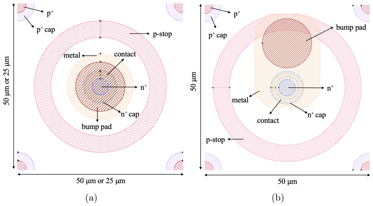
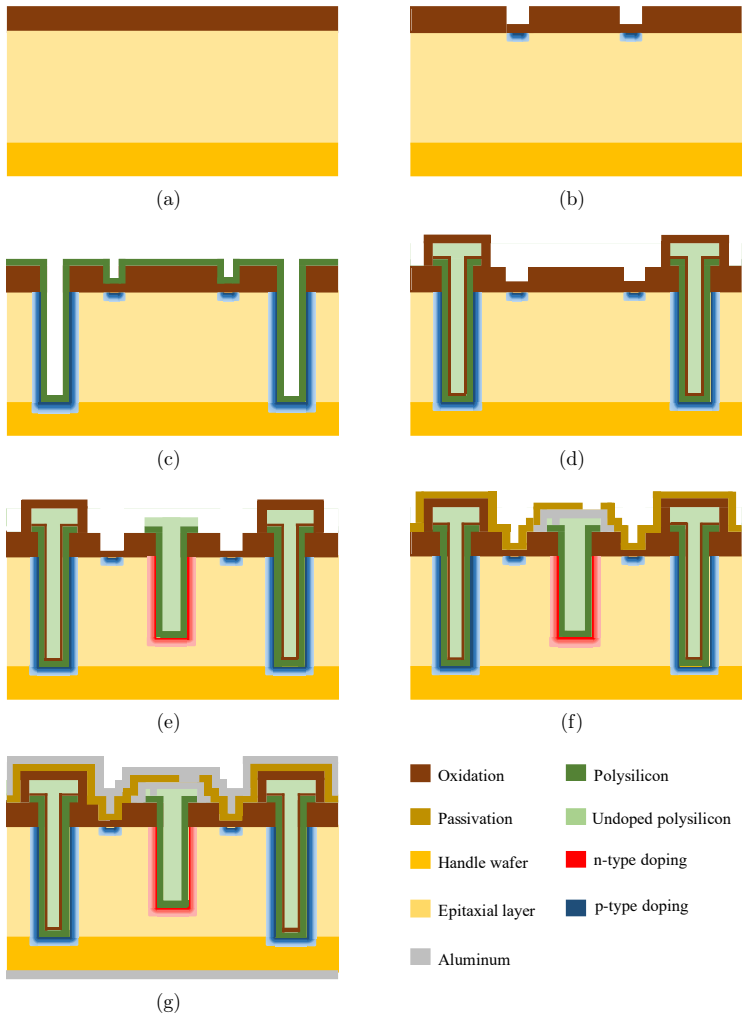
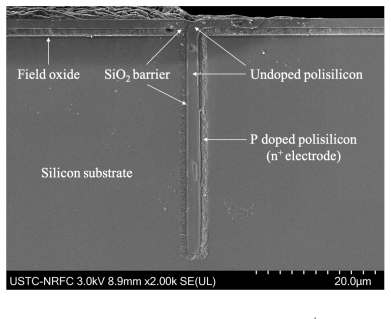
The paper establishes a fabrication process for 3D silicon sensors in which 5-micrometer-diameter columnar electrodes of both doping types are etched from the same side of a 50-micrometer epitaxial wafer; p+ columns traverse the full thickness while n+ columns terminate a short distance from the far surface, producing pixel arrays of 50 by 50 or 25 by 25 micrometers that are intended to record both position and arrival time at the single-pixel level.
What carries the argument
Asymmetric columnar electrode geometry in a 50-micrometer epitaxial silicon wafer, with through-going p+ columns and partial-depth n+ columns, combined with small-pitch pixel segmentation.
If this is right
- Particle trackers could record both hit position and time stamp from the same pixel, reducing the need for separate timing layers.
- The reduced active thickness lowers the material budget seen by traversing particles.
- Smaller pixel sizes increase spatial granularity while preserving the timing function.
- The single-side etch process simplifies production compared with double-sided 3D designs.
Where Pith is reading between the lines
- The same electrode layout could be applied to even thinner epitaxial layers if charge collection remains sufficient.
- Readout chips matched to the 25-micrometer pitch would be needed to exploit the full spatial resolution.
- Radiation-hardness studies on these thin structures would determine suitability for high-luminosity environments.
Load-bearing premise
The partial-depth n+ electrodes and the 50-micrometer thickness will still produce usable signals and timing resolution once the sensors are fully characterized.
What would settle it
Beam-test data showing either no detectable charge collection from the thin active volume or timing resolution worse than the target single-pixel value would disprove the design approach.
Figures


read the original abstract
We report on the development of 3D silicon sensors at the University of Science and Technology of China (USTC). The sensor involves columnar electrodes (5 um in diameter) of both doping types, etched from the same wafer side. The p+ electrodes pass through the epitaxial wafer, whereas the n+ electrodes stop at a short distance from the opposite side of the epitaxial wafer. With respect to previous generations of 3D sensors, they feature an ultra-thin active substrate (50 um) and a small pixel size of 50 um x 50 um or 25 um x 25 um. This R&D project aims to establish a sensor technology to simultaneously measure position and time information at the single-pixel level. The first run with one merged wafer layout has been completed. The design, fabrication, and characterization of the sensors are reported in this paper.
Editorial analysis
A structured set of objections, weighed in public.
Referee Report
Summary. The manuscript reports the development of ultra-thin 3D silicon sensors featuring 50 μm active thickness, 25×25 μm or 50×50 μm pixel pitches, and 5 μm diameter columnar electrodes of both doping types etched from the same side (p+ through-wafer, n+ partial depth). It describes the design, completion of the first fabrication run on a merged wafer layout, and characterization, with the stated goal of enabling simultaneous single-pixel position and timing measurements.
Significance. If the sensors ultimately demonstrate the targeted combined spatial and temporal resolution, the work would advance 3D sensor technology for applications such as high-luminosity collider detectors or fast-timing imaging by reducing active thickness and pixel size relative to prior generations. The manuscript itself supplies no performance data, so current significance is limited to the fabrication process description.
major comments (1)
- [Abstract and Characterization section] Abstract and Characterization section: The paper states that the first run is complete and that characterization is reported, yet no beam-test or laser-test results quantifying spatial resolution, timing jitter, time-walk, or hit efficiency are presented. Only process-monitoring data (e.g., IV/CV curves or optical inspection) appear to be included. This directly undermines the central claim that the geometry enables simultaneous position and time measurement at the single-pixel level.
minor comments (2)
- [Introduction] Introduction: Add explicit references to the most recent 3D sensor literature (e.g., prior ATLAS or CMS 3D pixel papers) to clarify the incremental improvements claimed for the 50 μm thickness and 25 μm pitch.
- [Figures] Figures: Ensure electrode cross-section diagrams include scale bars and explicit labels for the 5 μm diameter, 50 μm thickness, and partial n+ depth.
Simulated Author's Rebuttal
We thank the referee for the careful review and constructive feedback on our manuscript. We agree that the scope of the presented characterization requires clarification and have revised the text accordingly to better reflect the content of this first fabrication paper.
read point-by-point responses
-
Referee: [Abstract and Characterization section] Abstract and Characterization section: The paper states that the first run is complete and that characterization is reported, yet no beam-test or laser-test results quantifying spatial resolution, timing jitter, time-walk, or hit efficiency are presented. Only process-monitoring data (e.g., IV/CV curves or optical inspection) appear to be included. This directly undermines the central claim that the geometry enables simultaneous position and time measurement at the single-pixel level.
Authors: We agree with the referee that the manuscript reports only process-monitoring data (IV/CV curves and optical inspection) and does not contain beam-test or laser-test results on spatial resolution, timing jitter, time-walk or hit efficiency. The abstract and introduction describe the overall project goal of enabling simultaneous single-pixel position and timing measurements, but this paper focuses on the design and completion of the first fabrication run together with initial electrical characterization. We have revised the abstract to state explicitly that the reported characterization is limited to electrical and process-monitoring measurements, and we have added a sentence in the characterization section noting that beam and laser tests for position and timing performance are planned for a follow-up publication once the sensors are assembled with readout electronics. These changes remove any implication that the targeted combined resolution has already been demonstrated. revision: yes
Circularity Check
No circularity: experimental development report with no derivations or fitted predictions
full rationale
The paper is a straightforward experimental report on the design, fabrication process, and initial characterization (IV/CV curves, optical inspection) of ultra-thin 3D silicon sensors. No equations, parameter fits, or predictive derivations appear anywhere in the text. The central claims rest on physical fabrication steps and process monitoring data rather than any self-referential logic, self-citation chains, or renaming of known results. The absence of beam-test or timing-resolution numbers is a completeness issue, not a circularity issue. This matches the default expectation for non-circular experimental papers.
Axiom & Free-Parameter Ledger
Lean theorems connected to this paper
-
IndisputableMonolith/Foundation/RealityFromDistinction.leanreality_from_one_distinction unclear?
unclearRelation between the paper passage and the cited Recognition theorem.
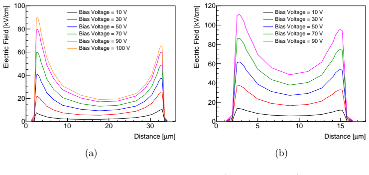
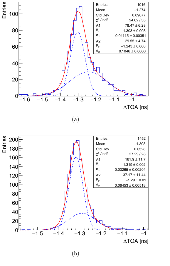
The sensor involves columnar electrodes (5 µm in diameter) of both doping types... ultra-thin active substrate (50 µm) and a small pixel size of 50 µm×50 µm or 25 µm×25 µm... time resolution... 31.08–63.75 ps
-
IndisputableMonolith/Cost/FunctionalEquation.leanwashburn_uniqueness_aczel unclear?
unclearRelation between the paper passage and the cited Recognition theorem.
Section 5 presents the results of the leakage current, breakdown voltage and time resolution.
What do these tags mean?
- matches
- The paper's claim is directly supported by a theorem in the formal canon.
- supports
- The theorem supports part of the paper's argument, but the paper may add assumptions or extra steps.
- extends
- The paper goes beyond the formal theorem; the theorem is a base layer rather than the whole result.
- uses
- The paper appears to rely on the theorem as machinery.
- contradicts
- The paper's claim conflicts with a theorem or certificate in the canon.
- unclear
- Pith found a possible connection, but the passage is too broad, indirect, or ambiguous to say the theorem truly supports the claim.
Reference graph
Works this paper leans on
-
[1]
C. Da Via, et al., 3D silicon sensors: Design, large area production and quality assurance for the ATLAS IBL pixel detector upgrade, Nucl. Instrum. Meth. A 694 (2012) 321–330. doi:10.1016/j.nima.2012.07. 058
-
[2]
Terzo, et al., Novel 3D Pixel Sensors for the Upgrade of the ATLAS Inner Tracker, Front
S. Terzo, et al., Novel 3D Pixel Sensors for the Upgrade of the ATLAS Inner Tracker, Front. Phys. Volume 9 - 2021 (2021). doi:10.3389/fphy. 2021.624668
-
[3]
Confinement and the center of the gauge group,
G. Kramberger, et al., Timing performance of small cell 3D silicon detectors, Nucl. Instrum. Meth. A 934 (2019) 26–32. doi:10.1016/j. nima.2019.04.088
work page doi:10.1016/j 2019
-
[4]
L. Diehl, et al., Evaluation of 3D sensors for fast timing applications, Nucl.Instrum.Meth.A1065(2024)169517.doi:10.1016/j.nima.2024. 169517
-
[5]
Parker, et al., Increased Speed: 3D Silicon Sensors; Fast Current Amplifiers, IEEE Trans
S. Parker, et al., Increased Speed: 3D Silicon Sensors; Fast Current Amplifiers, IEEE Trans. Nucl. Sci. 58 (2011) 404–417. doi:10.1109/ TNS.2011.2105889
-
[6]
Z. Li, New BNL 3D-Trench electrode Si detectors for radiation hard detectors for sLHC and for X-ray applications, Nucl. Instrum. Meth. A 658 (2011) 90–97. doi:10.1016/j.nima.2011.05.003, rESMDD 2010
-
[7]
Mendicino, et al., 3D trenched-electrode sensors for charged particle tracking and timing, Nucl
R. Mendicino, et al., 3D trenched-electrode sensors for charged particle tracking and timing, Nucl. Instrum. Meth. A 927 (2019) 24–30. doi:10. 1016/j.nima.2019.02.015
work page 2019
-
[8]
G. Forcolin, et al., 3D trenched-electrode pixel sensors: Design, tech- nology and initial results, Nucl. Instrum. Meth. A 981 (2020) 164437. doi:10.1016/j.nima.2020.164437. 23
-
[9]
D. Brundu, et al., Accurate modelling of 3D-trench silicon sensor with enhanced timing performance and comparison with test beam measure- ments, J. Instrum. 16 (2021) P09028. doi:10.1088/1748-0221/16/09/ P09028
-
[10]
F. Borgato, et al., Characterisation of highly irradiated 3D trench silicon pixel sensors for 4D tracking with 10 ps timing accuracy, Front. Phys 12 (2024). doi:10.3389/fphy.2024.1393019
-
[11]
Available at:https://www.synopsys.com/silicon/tcad
Synopsys Inc., Sentaurus Device User Guide Version L-2016.03, CA, USA, 2016. Available at:https://www.synopsys.com/silicon/tcad. html
work page 2016
-
[12]
J. T. Walton, F. S. Goulding, Silicon radiation detectors with oxide charge state compensation, IEEE Trans. Nucl. Sci. 34 (1987) 396–400. doi:10.1109/TNS.1987.4337370
-
[13]
F. Laermer, A. Schilp, Method of anisotropically etching silicon, US Patent No 5501893, 1996
work page 1996
- [14]
-
[15]
Bortfeldt, et al., Timing Performance of a Micro-Channel-Plate Photomultiplier Tube, Nucl
J. Bortfeldt, et al., Timing Performance of a Micro-Channel-Plate Photomultiplier Tube, Nucl. Instrum. Meth. A 960 (2020) 163592. doi:10.1016/j.nima.2020.163592. 24
discussion (0)
Sign in with ORCID, Apple, or X to comment. Anyone can read and Pith papers without signing in.