Recognition: no theorem link
Layer thickness dependent band gap of MBE grown single- to few-layer MoS₂
Pith reviewed 2026-05-14 17:57 UTC · model grok-4.3
The pith
MBE-grown MoS2 band gap shrinks below bulk value as layers increase from one to five.
A machine-rendered reading of the paper's core claim, the machinery that carries it, and where it could break.
Core claim
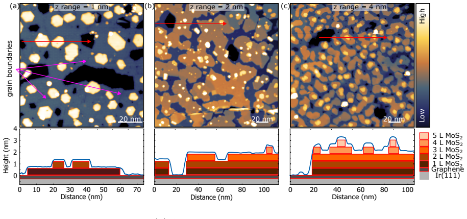
Scanning tunneling spectroscopy on molecular beam epitaxy grown MoS2 films on graphene on Ir(111) reveals a strong decrease in the band gap with increasing layer number from one to five, reaching values below the bulk band gap. The pinning of the conduction band edge disappears above four layers. Comparison with density functional theory and GW calculations indicates that the MBE growth conditions introduce additional screening responsible for the observed reduction.
What carries the argument
Additional screening from the molecular beam epitaxy growth conditions that overrides the standard layer-thickness dependence of the band gap.
If this is right
- The band gap of few-layer MoS2 can be reduced below the bulk value by selecting MBE growth rather than other fabrication methods.
- Conduction band pinning is absent in films thicker than four layers.
- Theoretical models of these films must incorporate growth-specific dielectric screening to match experimental gap values.
- Device engineering of MoS2 may need to treat substrate and growth history as additional tuning parameters for the gap.
Where Pith is reading between the lines
- The same growth-induced screening may allow similar downward tuning of gaps in other transition metal dichalcogenides produced by MBE.
- Experiments that swap growth methods while keeping the substrate fixed would isolate the contribution of MBE conditions from substrate effects.
- Measurements on films thicker than five layers could show whether the gap continues to narrow or eventually saturates.
Load-bearing premise
The measured reduction of the band gap below the bulk value is caused by extra screening from the MBE growth conditions rather than by interactions with the graphene/Ir(111) substrate or by systematic offsets when extracting band edges from tunneling spectra.
What would settle it
Repeating the scanning tunneling spectroscopy measurements on identical layer thicknesses of MoS2 grown by chemical vapor deposition on the same graphene/Ir(111) substrate and checking whether the gap still falls below the bulk value would test the claim.
Figures


read the original abstract
In light of the rise of transition metal dichalcogenides as 2D semiconductors for device applications, band engineering becomes very important from an application point of view. In many of these materials, such as the canonical example of MoS$_{2}$, the semiconductor band gap depends on the layer number. It changes from indirect to direct as it evolves from a bulk semiconductor to a monolayer. Interestingly, it was predicted and experimentally confirmed that, by thinning the material from bulk to a bilayer, the indirect transition shows a strong blue-shift. Here, we present the results of scanning tunnelling spectroscopy measurements on MoS$_{2}$ that has been grown \textit{in situ} via molecular beam epitaxy on graphene on Ir(111) at thicknesses ranging from 1 to 5 layers. We find a drastic decrease of the band gap with increasing layer number, to values even below the band gap in bulk. We also observe that the pinning of the conduction band vanishes above 4 layers. Comparing our experimental data with density functional theory and \textit{GW} calculations indicates that an additional screening is introduced by the sample growth conditions.
Editorial analysis
A structured set of objections, weighed in public.
Referee Report
Summary. The manuscript reports STS measurements on MBE-grown MoS2 from 1 to 5 layers on graphene/Ir(111), finding a strong decrease in band gap with layer number that reaches values below the bulk gap, with conduction-band pinning vanishing above 4 layers. The authors compare the data to DFT and GW calculations and attribute the sub-bulk gaps to extra screening introduced by the MBE growth conditions.
Significance. If the central interpretation is confirmed, the result would indicate that MBE-specific conditions can produce band-gap reductions in few-layer MoS2 beyond conventional layer-number trends, offering a potential handle for band engineering in TMD devices. The observation of gaps below bulk and the layer-dependent pinning behavior are noteworthy, though the absence of substrate controls weakens the causal link to growth conditions.
major comments (3)
- [Results] Results section: quantitative band-gap values, error bars, and the precise procedure for extracting conduction- and valence-band edges from the STS spectra are not provided, making it impossible to judge the statistical significance of the reported reduction below the bulk gap.
- [Discussion] Discussion section: the claim that the sub-bulk gaps arise from MBE-specific screening is not isolated from substrate effects; all STS data are acquired on the same graphene/Ir(111) surface with no control samples grown by other methods or on different substrates.
- [Theoretical comparison] Theoretical comparison: the DFT/GW calculations are not stated to incorporate the dielectric environment or possible charge transfer from the Ir(111) substrate, leaving open the possibility that the observed discrepancy with experiment originates from an incomplete model rather than additional MBE screening.
minor comments (2)
- [Abstract] Abstract: the statement that the gap decreases 'to values even below the band gap in bulk' is not accompanied by numerical values or figure references.
- [Figures] Figures: STS spectra should include explicit markers for extracted band edges and uncertainty estimates to improve readability.
Simulated Author's Rebuttal
We thank the referee for their careful reading and constructive comments. We address each major point below and have revised the manuscript to add quantitative details, clarify limitations, and improve the theoretical comparison where possible.
read point-by-point responses
-
Referee: [Results] Results section: quantitative band-gap values, error bars, and the precise procedure for extracting conduction- and valence-band edges from the STS spectra are not provided, making it impossible to judge the statistical significance of the reported reduction below the bulk gap.
Authors: We agree that the original manuscript lacked sufficient quantitative detail. In the revised version we now report the extracted band-gap values for each layer thickness together with error bars obtained from repeated measurements on multiple sample regions. We have also added an explicit description of the band-edge extraction procedure, which identifies the onset as the energy at which the dI/dV signal exceeds the noise floor by a factor of three and uses linear extrapolation of the rising edge. These additions permit a direct assessment of the statistical significance of the sub-bulk gaps. revision: yes
-
Referee: [Discussion] Discussion section: the claim that the sub-bulk gaps arise from MBE-specific screening is not isolated from substrate effects; all STS data are acquired on the same graphene/Ir(111) surface with no control samples grown by other methods or on different substrates.
Authors: We acknowledge that all data were acquired on graphene/Ir(111) and that control samples grown by other methods or on alternate substrates are not available. We have expanded the discussion to state this limitation explicitly and to compare our results with literature values for MoS2 prepared by CVD and mechanical exfoliation on a range of substrates, where gaps below the bulk value are not reported. While these comparisons support an MBE-specific contribution, we agree that substrate effects cannot be fully decoupled without additional experiments. revision: partial
-
Referee: [Theoretical comparison] Theoretical comparison: the DFT/GW calculations are not stated to incorporate the dielectric environment or possible charge transfer from the Ir(111) substrate, leaving open the possibility that the observed discrepancy with experiment originates from an incomplete model rather than additional MBE screening.
Authors: The calculations are performed for freestanding layers, as is conventional when isolating intrinsic layer-number trends. We have revised the text to state this explicitly and to note that substrate dielectric screening and possible charge transfer from Ir(111) are omitted. The remaining discrepancy with experiment is therefore attributed to additional screening arising from the MBE growth conditions. We have added a brief discussion of the desirability of future calculations that include the full substrate environment. revision: yes
Axiom & Free-Parameter Ledger
axioms (1)
- domain assumption Standard DFT and GW approximations are adequate for isolated MoS2 layers
Reference graph
Works this paper leans on
-
[1]
H., Kalantar-Zadeh, K., Kis, A., Coleman, J
Wang, Q. H., Kalantar-Zadeh, K., Kis, A., Coleman, J. N. & Strano, M. S. Electronics and optoelectronics of two-dimensional transition metal dichalcogenides.Nature Nanotechnology7, 699– 712 (2012)
work page 2012
-
[2]
Chhowalla, M.et al.The chemistry of two-dimensional layered transition metal dichalcogenide nanosheets.Nature Chemistry5, 263–275 (2013)
work page 2013
-
[3]
Butler, S. Z.et al.Progress, challenges, and opportunities in two-dimensional materials beyond graphene.ACS Nano7, 2898–2926 (2013)
work page 2013
-
[4]
Splendiani, A.et al.Emerging Photoluminescence in Monolayer MoS2.Nano Letters10, 1271–1275 (2010)
work page 2010
- [5]
-
[6]
Yin, Z.et al.Single-Layer MoS2 Phototransistors.ACS Nano6, 74–80 (2012)
work page 2012
-
[7]
Bernardi, M., Palummo, M. & Grossman, J. C. Extraordinary Sunlight Absorption and One Nanometer Thick Photovoltaics Using Two-Dimensional Monolayer Materials.Nano Letters13, 3664–3670 (2013)
work page 2013
-
[8]
Britnell, L.et al.Strong Light-Matter Interactions in Heterostructures of Atomically Thin Films. Science340, 1311–1314 (2013)
work page 2013
- [9]
-
[10]
Fuhr, J. D., Sa´ ul, A. & Sofo, J. O. Scanning Tunneling Microscopy Chemical Signature of Point De- fects on the${\mathrm{M}\mathrm{o}\mathrm{S}} {2}(0001)$Surface.Physical Review Letters 92, 026802 (2004)
work page 2004
-
[11]
Zou, X., Liu, Y. & Yakobson, B. I. Predicting Dislocations and Grain Boundaries in Two- Dimensional Metal-Disulfides from the First Principles.Nano Letters13, 253–258 (2013)
work page 2013
-
[12]
Zhou, W.et al.Intrinsic Structural Defects in Monolayer Molybdenum Disulfide.Nano Letters13, 2615–2622 (2013)
work page 2013
-
[13]
Yue, Q., Chang, S., Qin, S. & Li, J. Functionalization of monolayer MoS2 by substitutional doping: A first-principles study.Physics Letters A377, 1362–1367 (2013)
work page 2013
-
[14]
Jin, W.et al.Direct Measurement of the Thickness-Dependent Electronic Band Structure of ${\mathrm{MoS}} {2}$Using Angle-Resolved Photoemission Spectroscopy.Physical Review Let- ters111, 106801 (2013). 8
work page 2013
-
[15]
Zhang, Y.et al.Direct observation of the transition from indirect to direct bandgap in atomically thin epitaxial MoSe2.Nature Nanotechnology9, 111–115 (2014)
work page 2014
-
[16]
Komsa, H.-P. & Krasheninnikov, A. V. Effects of confinement and environment on the electronic structure and exciton binding energy of MoS${} {2}$from first principles.Physical Review B86, 241201 (2012)
work page 2012
-
[17]
Kuc, A., Zibouche, N. & Heine, T. Influence of quantum confinement on the electronic structure of the transition metal sulfide$T$S${} {2}$.Physical Review B83, 245213 (2011)
work page 2011
-
[18]
L.et al.Bandgap tunability at single-layer molybdenum disulphide grain boundaries
Huang, Y. L.et al.Bandgap tunability at single-layer molybdenum disulphide grain boundaries. Nature Communications6, 6298 (2015)
work page 2015
-
[19]
Bradley, A. J.et al.Probing the Role of Interlayer Coupling and Coulomb Interactions on Electronic Structure in Few-Layer MoSe2 Nanostructures.Nano Letters15, 2594–2599 (2015)
work page 2015
-
[20]
Trainer, D. J.et al.Inter-Layer Coupling Induced Valence Band Edge Shift in Mono- to Few-Layer MoS2.Scientific Reports7, 40559 (2017)
work page 2017
-
[21]
Murray, C.et al.Comprehensive tunneling spectroscopy of quasifreestanding ${\mathrm{MoS}} {2}$on graphene on Ir(111).Physical Review B99, 115434 (2019)
work page 2019
-
[22]
Castellanos-Gomez, A.et al.Local Strain Engineering in Atomically Thin MoS2.Nano Letters13, 5361–5366 (2013)
work page 2013
-
[23]
J.et al.Bandgap Engineering of Strained Monolayer and Bilayer MoS2.Nano Letters 13, 3626–3630 (2013)
Conley, H. J.et al.Bandgap Engineering of Strained Monolayer and Bilayer MoS2.Nano Letters 13, 3626–3630 (2013)
work page 2013
-
[24]
Feng, J., Qian, X., Huang, C.-W. & Li, J. Strain-engineered artificial atom as a broad-spectrum solar energy funnel.Nature Photonics6, 866–872 (2012)
work page 2012
-
[25]
Pan, H. & Zhang, Y.-W. Edge-dependent structural, electronic and magnetic properties of MoS2 nanoribbons.Journal of Materials Chemistry22, 7280–7290 (2012)
work page 2012
-
[26]
Liu, X., Balla, I., Bergeron, H. & Hersam, M. C. Point Defects and Grain Boundaries in Rotationally Commensurate MoS2 on Epitaxial Graphene.The Journal of Physical Chemistry C120, 20798– 20805 (2016)
work page 2016
-
[27]
Yan, C., Dong, X., Li, C. H. & Li, L. Charging effect at grain boundaries of MoS2.Nanotechnology 29, 195704 (2018)
work page 2018
-
[28]
Wang, D.et al.Bandgap broadening at grain boundaries in single-layer MoS2.Nano Research11, 6102–6109 (2018)
work page 2018
-
[29]
van Efferen, C.et al.Modulated Kondo screening along magnetic mirror twin boundaries in mono- layer MoS2.Nature Physics20, 82–87 (2024)
work page 2024
-
[30]
v.et al.Metal-insulator transition in monolayer MoS2 via contactless chemical doping
Efferen, C. v.et al.Metal-insulator transition in monolayer MoS2 via contactless chemical doping. 2D Materials9, 025026 (2022)
work page 2022
-
[31]
Mattheiss, L. F. Band structures of transition-metal-dichalcogenide layer compounds.Phys. Rev. B8, 3719–3740 (1973)
work page 1973
-
[32]
Lin, Y.-C., Dumcenco, D. O., Huang, Y.-S. & Suenaga, K. Atomic mechanism of the semiconducting- to-metallic phase transition in single-layered MoS2.Nature nanotechnology9, 391–396 (2014). 9
work page 2014
-
[33]
Balog, R.et al.Bandgap opening in graphene induced by patterned hydrogen adsorption.Nature Materials9, 315–319 (2010)
work page 2010
-
[34]
Xue, J.et al.Scanning tunnelling microscopy and spectroscopy of ultra-flat graphene on hexagonal boron nitride.Nature Materials10, 282–285 (2011)
work page 2011
-
[35]
Warmuth, J.et al.Band-gap engineering by bi intercalation of graphene on ir(111).Phys. Rev. B 93, 165437 (2016)
work page 2016
-
[36]
Hall, J.et al.Molecular beam epitaxy of quasi-freestanding transition metal disulphide monolayers on van der Waals substrates: a growth study.2D Materials5, 025005 (2018)
work page 2018
-
[37]
Fournel, F.et al.Molecular direct bonding and transfer of 2D MoS2 layer over a full 200 mm silicon wafer.Japanese Journal of Applied Physics64, 04SP49 (2025)
work page 2025
-
[38]
Ehlen, N.et al.Narrow photoluminescence and Raman peaks of epitaxial MoS2 on graphene/Ir(1 1 1).2D Materials6, 011006 (2018)
work page 2018
-
[39]
Growth kinetics of thin film epitaxy
Liu, H. Growth kinetics of thin film epitaxy. In Pham, P., Goel, P., Kumar, S. & Yadav, K. (eds.) 21st Century Surface Science - a Handbook, chap. 1 (IntechOpen, London, 2020)
work page 2020
-
[40]
Mortelmans, W.et al.On the van der waals epitaxy of homo-/heterostructures of transition metal dichalcogenides.ACS Applied Materials & Interfaces12, 27508–27517 (2020)
work page 2020
-
[41]
Schumann, H. & Schumann, I.Gmelin Handbook of Inorganic and Organometallic Chemistry - 8th edition(Springer-Verlag, 1995)
work page 1995
-
[42]
Esat, T.et al.Transfering spin into an extended pi orbital of a large molecule.Physical Review B 91, 144415 (2015)
work page 2015
-
[43]
Zhang, Y., Zhan, Z., Guinea, F., Silva-Guill´ en, J. A. & Yuan, S. Tuning band gaps in twisted bilayer Mos2.Phys. Rev. B102, 235418 (2020)
work page 2020
-
[44]
N’Diaye, A. T., Coraux, J., Plasa, T. N., Busse, C. & Michely, T. Structure of epitaxial graphene on Ir(111).New J. Phys.10, 043033 (2008)
work page 2008
-
[45]
Neˇ cas, D. & Klapetek, P. Gwyddion: an open-source software for SPM data analysis. centr.eur.j.phys.10, 181–188 (2012)
work page 2012
-
[46]
Dr¨ uppel, M.et al.Electronic excitations in transition metal dichalcogenide monolayers from an LDA+GdWapproach.Physical Review B98, 155433 (2018)
work page 2018
-
[47]
Electronic excitations from a perturbative LDA+GdW approach.Physical Review B 82, 205127 (2010)
Rohlfing, M. Electronic excitations from a perturbative LDA+GdW approach.Physical Review B 82, 205127 (2010)
work page 2010
-
[48]
J¨ ulich Supercomputing Centre. JUWELS Cluster and Booster: Exascale Pathfinder with Modular Supercomputing Architecture at Juelich Supercomputing Centre.Journal of large-scale research facilities7, A183 (2021). 10
work page 2021
discussion (0)
Sign in with ORCID, Apple, or X to comment. Anyone can read and Pith papers without signing in.