Layer-Polarization-Driven Metal-Insulator Transition in multi-band Graphene Moire' Superlattices
Pith reviewed 2026-06-27 21:19 UTC · model grok-4.3
The pith
A displacement field in trilayer graphene moiré superlattices drives layer polarization that selectively strengthens moiré coupling and opens a gap at the hole-doped secondary Dirac point.
A machine-rendered reading of the paper's core claim, the machinery that carries it, and where it could break.
Core claim
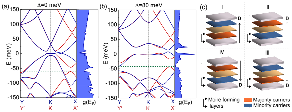
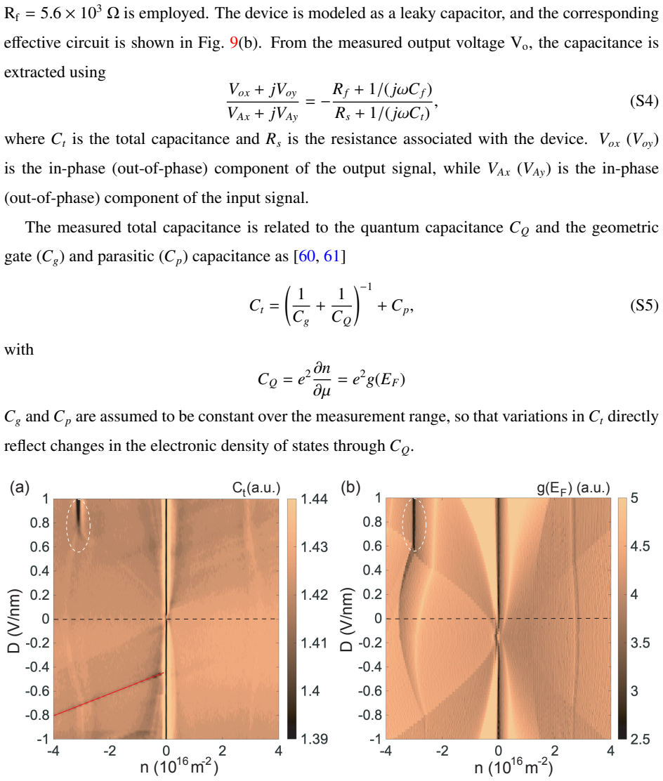
In ABA-stacked trilayer graphene moiré superlattices, increasing the perpendicular displacement field redistributes carriers across layers and selectively enhances their coupling to the extrinsic moiré potential. This drives a transition from a multi-band to an effectively single-band regime at low energies and opens a gap at the hole-doped secondary Dirac point, producing a metal-insulator transition. Quantum capacitance data show direct suppression of the density of states consistent with gap formation, and theoretical modeling identifies the layer-selective moiré coupling as the mechanism.
What carries the argument
Layer polarization induced by a perpendicular displacement field, which redistributes carriers to produce layer-selective coupling to the moiré potential.
If this is right
- Electrical tuning of layer polarization can switch the system between multi-band and single-band regimes at low energy.
- The same mechanism produces an electrically controlled insulating phase at the secondary Dirac point.
- Moiré potential hybridizes the massless and massive sectors of trilayer graphene when layer polarization is present.
- Layer-selective coupling supplies a route to engineer band gaps and correlated states in multi-band moiré systems.
Where Pith is reading between the lines
- The same displacement-field control may apply to other few-layer graphene stacks or different encapsulating materials to achieve similar band reconstruction.
- The resulting single-band regime at low energy could reduce interference from multiple bands when studying interaction-driven phases.
- Varying temperature or adding in-plane fields could test whether the induced gap remains stable or closes under conditions that weaken layer polarization.
Load-bearing premise
The observed suppression of density of states at the hole-doped secondary Dirac point is produced by a gap from displacement-induced layer-selective moiré coupling rather than disorder, interactions, or experimental artifacts.
What would settle it
Direct spectroscopy or capacitance measurements that show no gap opening when layer polarization is tuned while keeping the displacement field strength fixed, or that show the suppression persisting even when the moiré coupling is made layer-independent.
Figures






read the original abstract
Graphene/hBN moir\'e superlattices provide a highly tunable platform for exploring emergent quantum phases in low-dimensional systems. Here, we investigate the moir\'e superlattice formed between hBN and ABA-stacked trilayer graphene (TLG), an inherently multi-band system. We demonstrate that the moir\'e potential is not merely a perturbation but a tool to hybridize the distinct massless and massive electronic sectors of TLG. By applying a perpendicular displacement field to tune layer polarization, we drive a fundamental reconstruction of the electronic band structure. Specifically, increasing the displacement field evolves the system from a multi-band regime to an effectively single-band regime at low energies, accompanied by a metal--insulator transition at the hole-doped secondary Dirac point. This transition originates from a redistribution of carriers across graphene layers that selectively enhances their coupling to the extrinsic moir\'e potential. Quantum capacitance measurements provide direct evidence for the suppression of the density of states at the hole-side secondary Dirac point, consistent with gap opening and the emergence of a displacement-field-tuned band gap. Theoretical calculations reproduce these observations and identify layer-selective coupling to the moir\'e potential as the underlying mechanism. These results demonstrate electrical control of an emergent insulating phase in a low-dimensional moir\'e system, and highlight that layer polarization and layer-selective coupling in multi-band moir\'e heterostructures provide a powerful route for engineering topological and correlated phases through band structure reconstruction and electron interactions.
Editorial analysis
A structured set of objections, weighed in public.
Referee Report
Summary. The manuscript studies the hBN/ABA-trilayer graphene moiré superlattice and claims that a perpendicular displacement field drives layer polarization, converting the low-energy spectrum from multi-band to effectively single-band and opening a gap at the hole-doped secondary Dirac point. This produces a metal-insulator transition whose origin is identified as layer-selective enhancement of coupling to the extrinsic moiré potential. Quantum capacitance data are presented as direct evidence of DOS suppression, and theoretical calculations of the multi-band TLG Hamiltonian plus moiré term are said to reproduce the observations only when layer polarization is included.
Significance. If the central mechanistic attribution holds, the result supplies a concrete electrical knob (displacement-field-tuned layer polarization) for reconstructing bands and stabilizing an insulating phase in an inherently multi-band moiré platform. The explicit linkage between layer polarization, selective moiré coupling, and the observed capacitance dip would constitute a useful addition to the toolkit for engineering correlated states in graphene-based superlattices.
major comments (2)
- [Theoretical modeling section] Theoretical modeling section: the multi-band TLG Hamiltonian with extrinsic moiré potential is shown to open a gap at the hole-doped SDP once layer polarization is included, yet no explicit comparison is provided to interaction-driven scenarios (e.g., Hartree-Fock or Hubbard terms at the SDP) or to disorder broadening; if either alternative reproduces a comparable D-field dependence of the capacitance dip, the attribution to layer-selective moiré coupling remains under-determined.
- [Quantum capacitance measurements] Quantum capacitance data and interpretation: the central claim that the observed DOS suppression signals a displacement-field-induced gap from layer-selective moiré coupling (rather than disorder, interactions, or measurement artifacts) is load-bearing, but the manuscript supplies neither error bars, sample-quality metrics, nor explicit exclusion criteria that would rule out the competing mechanisms.
minor comments (2)
- Notation for the secondary Dirac point (hole-doped) is used inconsistently between abstract, figures, and text; a single symbol or label should be adopted.
- Figure captions should explicitly state the displacement-field values corresponding to each trace and whether the data are raw or background-subtracted.
Simulated Author's Rebuttal
We thank the referee for their careful reading and constructive comments on our manuscript. We address the two major comments point by point below, indicating where revisions will be made to strengthen the presentation.
read point-by-point responses
-
Referee: [Theoretical modeling section] Theoretical modeling section: the multi-band TLG Hamiltonian with extrinsic moiré potential is shown to open a gap at the hole-doped SDP once layer polarization is included, yet no explicit comparison is provided to interaction-driven scenarios (e.g., Hartree-Fock or Hubbard terms at the SDP) or to disorder broadening; if either alternative reproduces a comparable D-field dependence of the capacitance dip, the attribution to layer-selective moiré coupling remains under-determined.
Authors: We agree that an explicit comparison would make the mechanistic attribution more robust. Our minimal single-particle model demonstrates that gap opening at the hole-doped secondary Dirac point occurs only when the layer-polarization term is retained, because this term redistributes spectral weight and selectively amplifies the moiré matrix elements in the outer layers. Interaction-driven scenarios (Hartree-Fock or Hubbard) would require additional interaction parameters whose D dependence is not expected to track the layer polarization in the same way, while disorder broadening would produce a gradual smearing rather than a sharp, tunable suppression. Nevertheless, because the manuscript does not contain such side-by-side calculations, we will add a concise discussion paragraph (and, if space permits, a supplementary figure) that contrasts the expected D-field signatures of these alternatives with the layer-selective moiré mechanism. This constitutes a partial revision. revision: partial
-
Referee: [Quantum capacitance measurements] Quantum capacitance data and interpretation: the central claim that the observed DOS suppression signals a displacement-field-induced gap from layer-selective moiré coupling (rather than disorder, interactions, or measurement artifacts) is load-bearing, but the manuscript supplies neither error bars, sample-quality metrics, nor explicit exclusion criteria that would rule out the competing mechanisms.
Authors: The referee is correct that the manuscript does not display error bars on the capacitance traces or provide a dedicated methods paragraph on sample metrics and exclusion criteria. The raw data do show a systematic deepening of the capacitance dip with increasing displacement field, which is difficult to reconcile with static disorder or measurement artifacts. In the revised manuscript we will (i) add error bars derived from repeated sweeps and device-to-device variation, (ii) include a short characterization subsection reporting mobility, moiré period consistency, and contact quality, and (iii) add a paragraph that explicitly discusses why competing mechanisms are inconsistent with the observed D dependence. These additions will be made in the main text or supplementary information as appropriate. revision: yes
Circularity Check
No circularity; claims rest on independent experiment and modeling
full rationale
The abstract and context describe experimental quantum capacitance data interpreted via separate theoretical calculations of the multi-band TLG Hamiltonian with moiré potential. No quoted derivation reduces a prediction to a fitted parameter defined in terms of itself, nor does any load-bearing step rely on self-citation chains or ansatzes smuggled from prior author work. The layer-polarization mechanism is presented as an output of the modeling rather than an input by construction. This is the common case of a self-contained paper against external benchmarks.
Axiom & Free-Parameter Ledger
axioms (2)
- domain assumption Standard description of massless and massive bands in ABA trilayer graphene and layer polarization under perpendicular field
- domain assumption Moiré potential from hBN is extrinsic and can couple selectively to layers depending on carrier distribution
Reference graph
Works this paper leans on
-
[1]
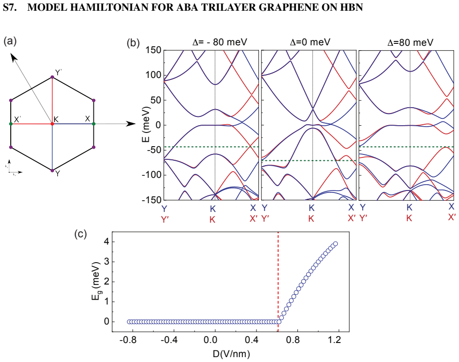
forT≥4 K (transport is dominated by variable range hopping below this temperature), and are plotted in Fig. 3(f). The extractedE g at the h-SDP remains below experimental resolution forD≤0.7 V/nm, after which it increases, reachingE g ∼1.4 meV atD=1.2 V/nm, demonstrating a displacement-field-induced opening of a tunable band gap. To summarize our primary ...
2019
-
[2]
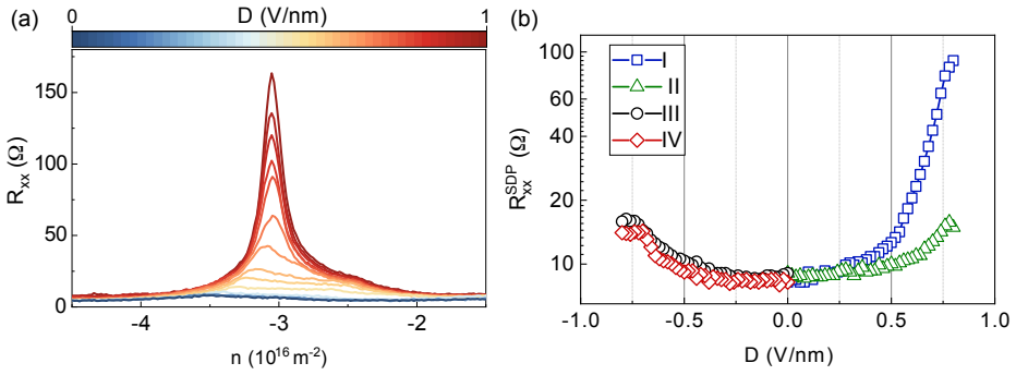
The magnitude ofR xx increases sharply in region I asDis increased above 0.6 V/nm, xiv (a) (c) (b) (d) h-SDP e-SDP I II IV III -4 -2 0 2 4 10 100 1000 Rxx (Ω) n (1016 m-2) -0.8 -0.4 0.0 0.4 0.8 2.2 2.4 2.6 2.8 I II III IV |ns| (1016 m-2) D (V/nm) -0.8 -0.4 0.0 0.4 0.8 50 500 100 1000 I II III IV RSDP XX (Ω) D (V/nm) n (1016 m-2) FIG. 6. (a) Log-scale plot...
-
[3]
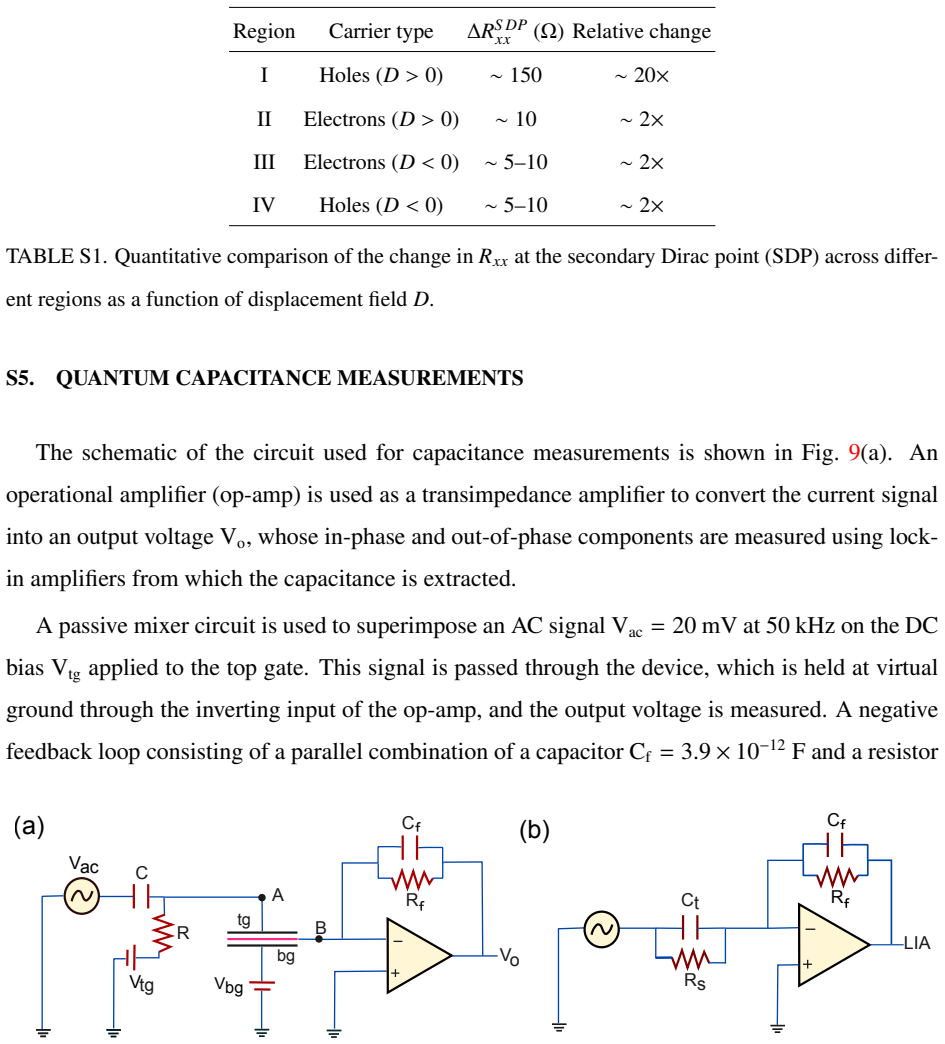
As|D|increases, the SDP shifts to lower carrier density. Fig. 6(c) shows a plot ofR S DP xx for regions I-IV as a function ofD. An asymmetry is observed betweenD>0 andD<0 at the h-SDP, whereas for e-SDP it remains largely symmetric. On the hole side,R S DP xx increases sharply from 32Ωto 425ΩasDis increased from 0 to 0.6 V/nm (blue open squares). In contr...
-
[4]
C.-H. Park, L. Yang, Y .-W. Son, M. L. Cohen, and S. G. Louie, Phys. Rev. Lett.101, 126804 (2008)
2008
-
[5]
Giovannetti, P
G. Giovannetti, P. A. Khomyakov, G. Brocks, P. J. Kelly, and J. van den Brink, Phys. Rev. B76, 073103 (2007)
2007
-
[6]
Decker, Y
R. Decker, Y . Wang, V . W. Brar, W. Regan, H.-Z. Tsai, Q. Wu, W. Gannett, A. Zettl, and M. F. Crommie, Nano Letters11, 2291 (2011)
2011
-
[7]
J. Xue, J. Sanchez-Yamagishi, D. Bulmash, P. Jacquod, A. Deshpande, K. Watanabe, T. Taniguchi, P. Jarillo-Herrero, and B. J. LeRoy, Nature materials10, 282 (2011)
2011
-
[8]
M. K. Jat, P. Tiwari, R. Bajaj, I. Shitut, S. Mandal, K. Watanabe, T. Taniguchi, H. Krishnamurthy, M. Jain, and A. Bid, Nature Communications15, 2335 (2024)
2024
-
[9]
Yankowitz, J
M. Yankowitz, J. Xue, D. Cormode, J. D. Sanchez-Yamagishi, K. Watanabe, T. Taniguchi, P. Jarillo- Herrero, P. Jacquod, and B. J. LeRoy, Nature physics8, 382 (2012)
2012
-
[10]
B. Hunt, J. D. Sanchez-Yamagishi, A. F. Young, M. Yankowitz, B. J. LeRoy, K. Watanabe, T. Taniguchi, P. Moon, M. Koshino, P. Jarillo-Herrero,et al., Science340, 1427 (2013)
2013
-
[11]
Ponomarenko, R
L. Ponomarenko, R. Gorbachev, G. Yu, D. Elias, R. Jalil, A. Patel, A. Mishchenko, A. Mayorov, C. Woods, J. Wallbank,et al., Nature497, 594 (2013)
2013
-
[12]
Gorbachev, J
R. Gorbachev, J. Song, G. Yu, A. Kretinin, F. Withers, Y . Cao, A. Mishchenko, I. Grigorieva, K. S. Novoselov, L. Levitov,et al., Science346, 448 (2014)
2014
-
[13]
Woods, L
C. Woods, L. Britnell, A. Eckmann, R. Ma, J. Lu, H. Guo, X. Lin, G. Yu, Y . Cao, R. V . Gorbachev, et al., Nature physics10, 451 (2014)
2014
-
[14]
G. Chen, A. L. Sharpe, E. J. Fox, Y .-H. Zhang, S. Wang, L. Jiang, B. Lyu, H. Li, K. Watanabe, T. Taniguchi,et al., Nature579, 56 (2020)
2020
-
[15]
Y . Cao, V . Fatemi, A. Demir, S. Fang, S. L. Tomarken, J. Y . Luo, J. D. Sanchez-Yamagishi, K. Watan- abe, T. Taniguchi, E. Kaxiras,et al., Nature556, 80 (2018)
2018
-
[16]
Serlin, C
M. Serlin, C. Tschirhart, H. Polshyn, Y . Zhang, J. Zhu, K. Watanabe, T. Taniguchi, L. Balents, and A. Young, Science367, 900 (2020)
2020
-
[17]
Y . Cao, V . Fatemi, S. Fang, K. Watanabe, T. Taniguchi, E. Kaxiras, and P. Jarillo-Herrero, Nature556, 43 (2018)
2018
-
[18]
Bistritzer and A
R. Bistritzer and A. H. MacDonald, Proceedings of the National Academy of Sciences108, 12233 (2011). xxix
2011
-
[19]
Balents, C
L. Balents, C. R. Dean, D. K. Efetov, and A. F. Young, Nature Physics16, 725 (2020)
2020
-
[20]
G. Chen, A. L. Sharpe, P. Gallagher, I. T. Rosen, E. J. Fox, L. Jiang, B. Lyu, H. Li, K. Watanabe, T. Taniguchi,et al., Nature572, 215 (2019)
2019
-
[21]
A. L. Sharpe, E. J. Fox, A. W. Barnard, J. Finney, K. Watanabe, T. Taniguchi, M. Kastner, and D. Goldhaber-Gordon, Science365, 605 (2019)
2019
-
[22]
W. Zhou, J. Ding, J. Hua, L. Zhang, K. Watanabe, T. Taniguchi, W. Zhu, and S. Xu, Nature Commu- nications15, 2597 (2024)
2024
-
[23]
B. Zhou, H. Yang, and Y .-H. Zhang, Phys. Rev. Lett.133, 206504 (2024)
2024
-
[24]
H. Peng, J. Zhong, Q. Feng, Y . Hu, Q. Li, S. Zhang, J. Mao, J. Duan, and Y . Yao, Communications Physics7, 240 (2024)
2024
-
[25]
Shavit, E
G. Shavit, E. Berg, A. Stern, and Y . Oreg, Phys. Rev. Lett.127, 247703 (2021)
2021
-
[26]
B. Wu, H. Zheng, S. Li, J. Ding, J. He, Y . Zeng, K. Chen, Z. Liu, S. Chen, A. Pan,et al., Light: Science & Applications11, 166 (2022)
2022
-
[27]
Xiong, J
R. Xiong, J. H. Nie, S. L. Brantly, P. Hays, R. Sailus, K. Watanabe, T. Taniguchi, S. Tongay, and C. Jin, Science380, 860 (2023)
2023
-
[28]
P. C. Adak, S. Sinha, A. Agarwal, and M. M. Deshmukh, Nature Reviews Materials9, 481 (2024)
2024
-
[29]
J. R. Wallbank, A. A. Patel, M. Mucha-Kruczy ´nski, A. K. Geim, and V . I. Fal’ko, Phys. Rev. B87, 245408 (2013)
2013
-
[30]
M. K. Jat, S. Mishra, H. K. Mann, R. Bajaj, K. Watanabe, T. Taniguchi, H. R. Krishnamurthy, M. Jain, and A. Bid, Nano Letters24, 2203 (2024)
2024
-
[31]
M. K. Jat, K. Watanabe, T. Taniguchi, and A. Bid, Phys. Rev. B113, L081102 (2026)
2026
-
[32]
Tiwari, K
P. Tiwari, K. Watanabe, T. Taniguchi, and A. Bid, Phys. Rev. B110, 235414 (2024)
2024
-
[33]
Moon and M
P. Moon and M. Koshino, Physical Review B90, 155406 (2014)
2014
-
[34]
N. Dale, M. I. B. Utama, D. Lee, N. Leconte, S. Zhao, K. Lee, T. Taniguchi, K. Watanabe, C. Jozwiak, A. Bostwick, E. Rotenberg, R. J. Koch, J. Jung, F. Wang, and A. Lanzara, Nano Letters23, 6799 (2023)
2023
-
[35]
S. H. Aronson, T. Han, Z. Lu, Y . Yao, J. P. Butler, K. Watanabe, T. Taniguchi, L. Ju, and R. C. Ashoori, Phys. Rev. X15, 031026 (2025)
2025
-
[36]
A. A. Zibrov, C. Kometter, H. Zhou, E. Spanton, T. Taniguchi, K. Watanabe, M. Zaletel, and A. Young, Nature549, 360 (2017)
2017
-
[37]
Mukai, K
F. Mukai, K. Horii, R. Ebisuoka, K. Watanabe, T. Taniguchi, and R. Yagi, Communications Physics4, xxx 109 (2021)
2021
-
[38]
W. Bao, L. Jing, J. Velasco Jr, Y . Lee, G. Liu, D. Tran, B. Standley, M. Aykol, S. Cronin, D. Smirnov, et al., Nature Physics7, 948 (2011)
2011
-
[39]
C. H. Lui, Z. Li, K. F. Mak, E. Cappelluti, and T. F. Heinz, Nature Physics7, 944 (2011)
2011
-
[40]
M. G. Menezes, R. B. Capaz, and S. G. Louie, Phys. Rev. B89, 035431 (2014)
2014
-
[41]
S. Kaur, H. Singh, K. Watanabe, T. Taniguchi, U. Ghorai, M. Jain, R. Sensarma, and A. Bid, Phys. Rev. Lett.135, 206501 (2025)
2025
-
[42]
H. K. Mann, S. Kaur, S. Mullick, P. Tiwari, K. Watanabe, T. Taniguchi, and A. Bid, Phys. Rev. B111, 235118 (2025)
2025
-
[43]
S. Kaur, U. Ghorai, A. Samanta, K. Watanabe, T. Taniguchi, R. Sensarma, and A. Bid, Phys. Rev. B 112, L161103 (2025)
2025
- [44]
-
[45]
Serbyn and D
M. Serbyn and D. A. Abanin, Phys. Rev. B87, 115422 (2013)
2013
-
[46]
Koshino and E
M. Koshino and E. McCann, Phys. Rev. B79, 125443 (2009)
2009
-
[47]
Rao and M
P. Rao and M. Serbyn, Phys. Rev. B101, 245411 (2020)
2020
-
[48]
A. A. Avetisyan, B. Partoens, and F. M. Peeters, Phys. Rev. B80, 195401 (2009)
2009
-
[49]
Z. Zhu, S. Carr, Q. Ma, and E. Kaxiras, Phys. Rev. B106, 205134 (2022)
2022
-
[50]
Castellanos-Gomez, M
A. Castellanos-Gomez, M. Buscema, R. Molenaar, V . Singh, L. Janssen, H. S. J. van der Zant, and G. A. Steele, 2D Materials1, 011002 (2014)
2014
-
[51]
Serbyn and D
M. Serbyn and D. A. Abanin, Physical Review B87, 115422 (2013)
2013
-
[52]
Taychatanapat, K
T. Taychatanapat, K. Watanabe, T. Taniguchi, and et al., Nature Physics7, 621 (2011)
2011
-
[53]
M. S. Dresselhaus and G. Dresselhaus, Advances in Physics51, 1 (2002)
2002
-
[54]
Koshino and E
M. Koshino and E. McCann, Phys. Rev. B81, 115315 (2010)
2010
-
[55]
J. C. Slonczewski and P. R. Weiss, Phys. Rev.109, 272 (1958)
1958
-
[56]
Kindermann, B
M. Kindermann, B. Uchoa, and D. L. Miller, Phys. Rev. B86, 115415 (2012)
2012
-
[57]
Moon and M
P. Moon and M. Koshino, Phys. Rev. B87, 205404 (2013)
2013
-
[58]
S. Kaur, T. Chanda, K. R. Amin, D. Sahani, K. Watanabe, T. Taniguchi, U. Ghorai, Y . Gefen, G. J. Sreejith, and A. Bid, Nature Communications15, 8535 (2024)
2024
-
[59]
Y . Yang, J. Li, J. Yin, S. Xu, C. Mullan, T. Taniguchi, K. Watanabe, A. K. Geim, K. S. Novoselov, and A. Mishchenko, Science Advances6, eabd3655 (2020). xxxi
2020
-
[60]
D. R. Hofstadter, Phys. Rev. B14, 2239 (1976)
1976
-
[61]
R. K. Kumar, X. Chen, G. H. Auton, A. Mishchenko, D. A. Bandurin, S. V . Morozov, Y . Cao, E. Khes- tanova, M. B. Shalom, A. V . Kretinin, K. S. Novoselov, L. Eaves, I. V . Grigorieva, L. A. Ponomarenko, V . I. Fal’ko, and A. K. Geim, Science357, 181 (2017)
2017
-
[62]
L. Wang, S. Zihlmann, M.-H. Liu, P. Makk, K. Watanabe, T. Taniguchi, A. Baumgartner, and C. Schö- nenberger, Nano Letters19, 2371 (2019)
2019
-
[63]
Luryi, Applied Physics Letters52, 501 (1988)
S. Luryi, Applied Physics Letters52, 501 (1988)
1988
-
[64]
Ilani, L
S. Ilani, L. A. Donev, M. Kindermann, and P. L. McEuen, Nature Physics2, 687 (2006)
2006
-
[65]
Bistritzer and A
R. Bistritzer and A. H. MacDonald, Phys. Rev. B84, 035440 (2011)
2011
-
[66]
J. W. McClure, Phys. Rev.104, 666 (1956)
1956
-
[67]
Ando, Journal of the Physical Society of Japan74, 777 (2005)
T. Ando, Journal of the Physical Society of Japan74, 777 (2005)
2005
-
[68]
Sławi ´nska, I
J. Sławi ´nska, I. Zasada, and Z. Klusek, Phys. Rev. B81, 155433 (2010)
2010
-
[69]
Koshino and E
M. Koshino and E. McCann, Phys. Rev. B80, 165409 (2009). xxxii
2009
discussion (0)
Sign in with ORCID, Apple, or X to comment. Anyone can read and Pith papers without signing in.