REVIEW 5 major objections 5 minor 50 references
Imaging van Hove Singularity Heterogeneity in Overdoped Graphene
T0 review · 5 major / 5 minor · reviewed 2026-08-08 · deepseek-v4-flash
Pith's one-line read Two distinct Yb dopant species make the van Hove singularity position in overdoped graphene vary on a 3-nm scale, so the material is electronically patchy rather than uniformly doped.
desk verdict First real-space vHS maps in overdoped graphene are the real deal; the substitutional-Yb claim is plausible but under-supported. read the letter →
The pith
A machine-rendered reading of the paper's core claim, the machinery that carries it, and where it could break.
The reading
What carries the argument
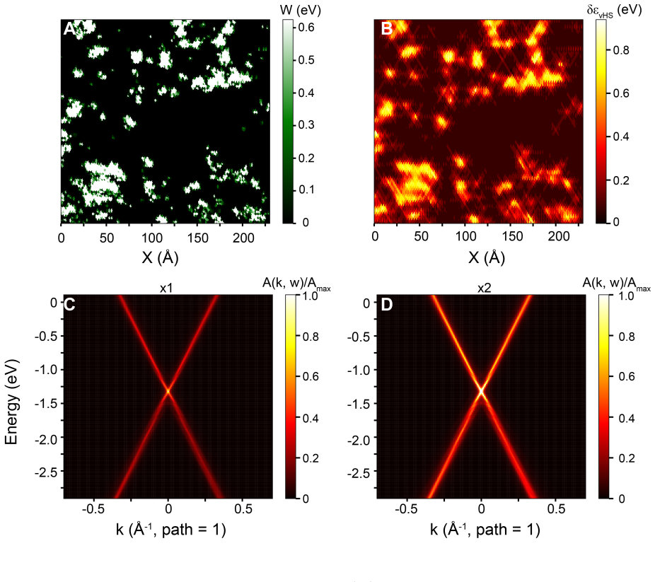
The paper's central objects are the spatially resolved van Hove singularity position $E_{\text{vHS}}(\mathbf{r})$, extracted pixel-by-pixel from $dI/dV$ spectra, and the differential conductance map at the Yb $4f$-state energy, $g(\mathbf{r}, E=-800\,\text{meV})$, which marks the substitutional Yb sites. The mechanism that carries the argument is a local Gaussian potential model: each Yb atom, whether intercalated or substitutional, is represented by a potential $W \exp(-r^2/(2\sigma^2))$, and the tight-binding local density of states computed with these potentials reproduces both the measured vHS shifts and the ARPES broadening.
What would settle it
Element-specific imaging of the same sample—for example, synchrotron-based X-ray scanning tunneling microscopy or atom probe tomography that chemically identifies the bright spots at -800 meV—would settle the claim. If those spots turned out to be carbon vacancies, residual contaminants, or silicon from the substrate, the two-mechanism picture would lose its substitutional-Yb component.
Extended reading notes
Core claim
The central claim is that overdoped graphene produced by Yb intercalation on SiC is not a uniformly doped metal but a patchwork of regions with different van Hove singularity energies. Two populations of Yb atoms are responsible. Most Yb atoms intercalate between graphene and the SiC substrate and donate electrons, moving the vHS toward the Fermi level, but their spatial distribution is uneven, and the resulting doping variations are screened over roughly 3 nm. A minority of Yb atoms become substitutional, embedded in the graphene basal plane; these act as strong local scatterers that push the vHS away from the Fermi level, suppress the quasiparticle amplitude, and broaden the spectral function, reproducing the ARPES linewidths. The spatially resolved vHS map correlates directly with the positions of the bright impurity states seen at -800 meV, and a tight-binding model with local Gaussian potentials placed at those sites reproduces the observed vHS shifts.
Load-bearing premise
The assignment of the bright spots in the conductance map at -800 meV to substitutional Yb atoms in the graphene basal plane rests on indirect evidence, because no atomically resolved chemical identification distinguishes Yb from other possible impurities.
Editorial extensions
If this is right
- Studies that treat Yb-intercalated graphene as uniformly doped will miss the nanoscale patchwork, because transport and spectroscopic averages mix regions with different vHS energies.
- The vHS peak amplitude is positively correlated with its energy position, so a rigid-band-shift description of overdoped graphene is insufficient; interaction and disorder effects must be included.
- The coexistence of intercalated and substitutional dopants means the total dopant density alone does not determine the local electronic structure.
- Theoretical calculations of correlated phases near the vHS should use disorder profiles rather than uniform doping to predict where such phases could nucleate.
- The roughly 3 nm screening length sets the scale over which local doping variations are felt, providing a concrete length scale for nanoscale electronic texture in graphene.
Reading between the lines
- A similar two-species coexistence may occur in other lanthanide-intercalated graphene systems (for example, Er or Tb) and in other two-dimensional materials where metal atoms can both intercalate and substitute, potentially making electronic inhomogeneity a general feature rather than a Yb-specific quirk.
- If nanoscale regions with the vHS close to the Fermi level are real, they are natural places to search for emergent superconductivity or charge order; local probes at lower temperature could test this.
- The positive correlation between vHS amplitude and position hints that interactions, not just disorder, are at play; momentum-resolved STM or quasiparticle interference measurements could reveal the interaction channel.
- The Gaussian-potential disorder model reconciles ARPES and STM, but its parameters were fit to a single field of view; testing it on multiple areas and on samples with different Yb coverage would show whether the 3 nm scale is universal.
Signed reviews
Editorial analysis
A structured set of objections, weighed in public.
Referee Report
Summary. This manuscript reports an in-situ ARPES and SI-STM study of Yb-intercalated quasi-freestanding monolayer graphene grown on SiC. The authors map the local energy position of the van Hove singularity (vHS) and observe significant spatial heterogeneity, which they attribute to two mechanisms: (i) spatial variations in the doping caused by inhomogeneously distributed intercalated Yb atoms, with a characteristic screening length of about 3 nm, and (ii) strong local perturbations from substitutional Yb atoms in the graphene basal plane. A tight-binding model with local Gaussian potentials, whose parameters are matched to the experimental data, is used to reproduce the vHS map and the ARPES band broadening.
Significance. The direct spatial mapping of vHS energy variations is a valuable and relatively novel experimental contribution, and the in-situ combination of ARPES and STM on the same surface is a clear strength of the paper. If the two-mechanism picture is confirmed, the work would establish that heavily doped graphene near a vHS should be treated as a spatially inhomogeneous electronic system, with implications for interpreting transport, spectroscopic, and potential correlated-phase experiments. However, the chemical identification of substitutional Yb is indirect, and the theoretical confirmation is weakened by parameter fitting against the same data from which the disorder profile is constructed. The core qualitative observation is interesting, but the paper's strongest claim is not yet fully supported.
major comments (5)
- [Fig. 3B and 'In STM...'] The assignment of the ~50 bright spots in g(r, E = -800 meV) to substitutional Yb atoms is not directly established. The arguments presented - the spot count being far below the total doping density and the absence of similar features in undoped graphene - exclude neither other Yb-induced defects nor contamination. Because the second mechanism (substitutional Yb in the basal plane) carries a large part of the paper's conclusion, this identification is load-bearing. The authors should provide direct chemical or atomic-structural evidence (e.g., atomically resolved STM simulations of substitutional Yb, X-ray photoelectron spectroscopy, or a characteristic signature in the topographic image) or clearly reframe the claim as tentative.
- [Section II (Theoretical Model Description) and Fig. 6] The model confirmation is partly circular. The disorder profile in Fig. 5A is constructed from the same g(r, -800 meV) map used to identify the impurities, W is estimated from the maximum LDOS shift generated by the same Gaussian potential, and sigma is selected by maximizing the cross-correlation between the simulated and experimental vHS maps. The resulting peak cross-correlation is only ~0.16, which the authors themselves call weak. This does not support the statement that the theoretical approach 'well captures' the experimental map. Please provide an out-of-sample test or a null-model comparison (e.g., random disorder profiles with the same density) to quantify the predictive power of the model.
- [Abstract and Sec. II (sample characterization)] The abstract states that the chemical potential is shifted to within 250 meV of the vHS, while Fig. 2E shows the vHS peak at 400 meV above the Fermi level and the Dirac point 1.4 eV below it. This discrepancy should be reconciled: either the 400 meV peak is not the vHS, or the 'within 250 meV' statement is incorrect.
- [Fig. 3D and accompanying text] The claim that the vHS peak amplitude increases with peak position, indicating interaction effects beyond a rigid band shift, is interesting; however, the correlation is reported only qualitatively. Please provide a quantitative correlation coefficient and error bars, and specify how the vHS position was extracted (e.g., fitting procedure, energy resolution) so the reader can assess the significance.
- [Section II (Theoretical Model Description)] The model assumes the same Gaussian potential amplitude W and width sigma for both substitutional and intercalated Yb atoms. This is an ad hoc assumption with no physical justification, and since W and sigma are fit to the data, the model cannot separately validate the two mechanisms. A sensitivity analysis or separate treatment of the two species would strengthen the claim.
minor comments (5)
- [Throughout] There are several typos: 'substitional' and 'subsitutional' should be 'substitutional', 'inhomogenity' should be 'inhomogeneity', and 'Inhonomgenous' in the caption of Fig. 3 should be corrected.
- [References] Reference [36] is cited as 'Emstev et al.' in the text; the correct spelling is 'Emtsev et al.'.
- [Fig. 2 callouts] The text referring to Figure 2 is inconsistent: 'Figure 2D represents a zoomed-in image of the area in Figure 2C marked by the white box' appears to refer to the topography panel, not the Fermi surface shown in Fig. 2C. Please correct the figure callouts.
- [Fig. 7-9 callouts] The sentence 'We take a supercell consisting of 82 x 82 unit cells which cover some of the substitutional/intercalated Yb profile shown in Figure 5A, upper panel of Figure 7, 8, and 9' is confusing because Figures 7-9 are not called out in order elsewhere. Please clarify which panels are being referenced.
- [Fig. 5 caption] The caption of Fig. 5 states that the nearest-neighbor hopping parameter t is set to 3 eV and the finite strip is 200 x 200 unit cells, but the text in Section II mentions both 200 x 200 and 82 x 82 supercells; please ensure the caption is consistent with the methods.
Circularity Check
The theoretical vHS-map 'confirmation' is partly a fit: W and σ are calibrated to the experimental vHS data, and the disorder positions come from the same g(r, -800 meV) map used to identify the impurities.
-
fitted input called prediction
[Main text, paragraph beginning 'In order to further corroborate...' (Figs. 5-6); also Section II 'Theoretical Model Description'.]
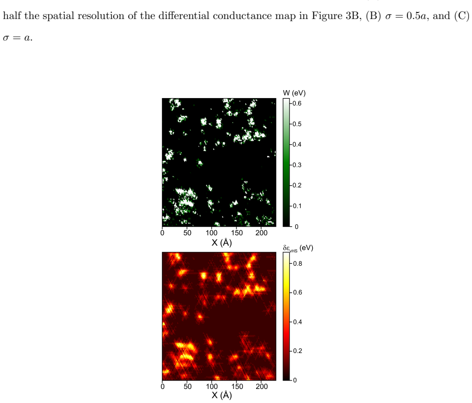
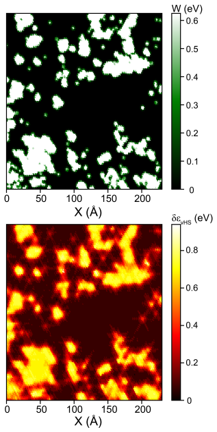
"The position of the substitutional/intercalated Yb atom is identified from the differential conductance map presented in Figure 3B and the value of W is estimated by assessing the maximum shift of LDOS (as in Figure 1A) created by the single Gaussian potential. The resultant disorder profile is shown in Figure 5A. ... We chose the intermediate value of σ based on cross-correlation analysis between the simulated and experimental vHS maps presented in Figure 6 as the highest cross-correlation is obtained between theory and experiment when σ is equal to 0.5a. ..."
The quantitative match between the simulated and experimental vHS maps is not an independent prediction: W is set from the observed maximum LDOS/vHS shift, σ is selected by maximizing cross-correlation against the same experimental vHS map, and the disorder positions are taken from the g(r, -800 meV) map that was already used to identify the impurity sites. The computed vHS shift therefore inherits its amplitude and length scale from the data it is said to confirm. The paper itself states that the peak cross-correlation is only about 0.16 and 'does not indicate a strong correlation,' so the confirmatory value of this comparison is limited.
full rationale
The paper's main experimental finding—spatially heterogeneous vHS position in overdoped graphene with a roughly 3 nm screening length and localized bright spots at -800 meV—is a direct measurement and does not by itself reduce to a fit. No load-bearing self-citation or imported uniqueness theorem is present; the cited prior work is external and independent. The only substantial circularity is in the theoretical confirmation: the Gaussian-disorder model is calibrated to the very vHS and conductance maps it is then said to reproduce, so the claim that 'theoretical calculations confirm' the mechanism is partly a restatement of the fit. The indirect assignment of bright spots to substitutional Yb is an evidentiary weakness rather than a circular derivation, since the identification is not made through the model. Overall, the central observation stands on its own, but the quantitative theoretical corroboration is partially circular; hence a score of 6 rather than higher.
Assumptions & free parameters
free parameters (2)
- W (Gaussian potential amplitude) =
0.63 eV
- sigma (Gaussian potential width) =
0.5a = 0.71 Å
assumptions (4)
- domain assumption Monolayer graphene on SiC can be treated as quasi-free-standing with a simple nearest-neighbor tight-binding band structure.
- ad hoc to paper The effect of both substitutional and intercalated Yb atoms is captured by a local Gaussian potential W exp(-r^2/(2 sigma^2)) with the same W and sigma for both types.
- domain assumption The bright spots in the conductance map at -800 meV are substitutional Yb atoms.
- domain assumption The spatially averaged doping density measured by ARPES applies to the small STM field of view.
invented entities (1)
-
Substitutional Yb atoms in the graphene basal plane
Cite this review
Pith. "Pith review of Imaging van Hove Singularity Heterogeneity in Overdoped Graphene." pith.science (2026). https://pith.science/paper/35YKANNZ
@misc{pith2026250207899,
  author       = {Pith},
  title        = {Pith review of: Imaging van Hove Singularity Heterogeneity in Overdoped Graphene},
  year         = {2026},
  howpublished = {\url{https://pith.science/paper/35YKANNZ}},
  note         = {Machine review of arXiv:2502.07899}
}
read the original abstract
Tuning the chemical potential of a solid to the vicinity of a van Hove singularity (vHS) is a well-established route to discovering emergent quantum phases. In monolayer graphene, the use of electron-donating metal layers has recently emerged as a method to dope the chemical potential to the nearest vHS, as evidenced by Angle-Resolved Photoemission Spectroscopy (ARPES) measurements. In this work, we study the spatial uniformity of the doping from this process using spectroscopic imaging scanning tunneling microscopy (SI-STM). Using molecular beam epitaxy (MBE), we achieve electron doping of graphene on SiC using Ytterbium (Yb-Graphene). We show using in-situ ARPES that the chemical potential is shifted to within 250 meV of the vHS. Using in-situ SI-STM, we establish that there exists significant inhomogeneity in the vHS position in overdoped graphene. We find two separate reasons for this. First, the spatial inhomogeneity of the intercalated Yb leads to local variations in the doping, with a length scale of inhomogeneity set by the screening length of ~ 3 nm. Second, we observe the presence of substitutional Yb dopants in the graphene basal plane. These Yb dopants cause a strong local shift of the doping, along with a renormalization of the quasiparticle amplitude. Theoretical calculations confirm that the Yb impurities effectively change the local potential, thus energetically shifting the position of the van Hove singularity. Our results point to the importance of considering the spatial structure of doping and its inextricable link to electronic structure.
Figures


Figures from the paper (6 more)



Reference graph
Works this paper leans on
-
[1]
H. Liu, Y. Liu, and D. Zhu, Chemical doping of graphene, J. Mater. Chem. 21, 3335 (2011), publisher: The Royal Society of Chemistry. 11
work page 2011
-
[2]
W. Chen, D. Qi, X. Gao, and A. T. S. Wee, Surface transfer doping of semiconductors, Progress in Surface Science 84, 279 (2009)
work page 2009
-
[3]
carbon buffer layer leads to a carrier density of ∼ 2.4 ∗ 1014cm−2. Unlike the Fermi surface of pristine graphene with two triangular electron pockets centered on the K and K ′ points, there is substan- tial trigonal warping leading to increased intensity along the KMK’ direction, which is an indication of an extended vHS. A high-resolution energy-momentu...
-
[4]
N. Jung, N. Kim, S. Jockusch, N. J. Turro, P. Kim, and L. Brus, Charge transfer chemical doping of few layer graphenes: Charge distribution and band gap formation, Nano Letters 9, 4133 (2009), pMID: 19827759, https://doi.org/10.1021/nl902362q
-
[5]
A. C. Crowther, A. Ghassaei, N. Jung, and L. E. Brus, Strong charge-transfer dop- ing of 1 to 10 layer graphene by no2, ACS Nano 6, 1865 (2012), pMID: 22276666, https://doi.org/10.1021/nn300252a
-
[6]
M. Bokdam, P. A. Khomyakov, G. Brocks, Z. Zhong, and P. J. Kelly, Electrostatic doping of graphene through ultrathin hexagonal boron nitride films, Nano Letters 11, 4631 (2011), pMID: 21936569, https://doi.org/10.1021/nl202131q
-
[7]
J. E. Padilha, A. Fazzio, and A. J. R. da Silva, van der waals heterostructure of phosphorene and graphene: Tuning the schottky barrier and doping by electrostatic gating, Phys. Rev. Lett. 114, 066803 (2015)
work page 2015
-
[8]
S.-F. Shi, T.-T. Tang, B. Zeng, L. Ju, Q. Zhou, A. Zettl, and F. Wang, Controlling graphene ultrafast hot carrier response from metal-like to semiconductor-like by electrostatic gating, Nano Letters 14, 1578 (2014), pMID: 24564302, https://doi.org/10.1021/nl404826r
Show all 50 references
-
[9]
Zhang, T.-T
Y. Zhang, T.-T. Tang, C. Girit, Z. Hao, M. C. Martin, A. Zettl, M. F. Crommie, Y. R. Shen, and F. Wang, Direct observation of a widely tunable bandgap in bilayer graphene, Nature 459, 820 (2009)
2009
-
[10]
Bistritzer and A
R. Bistritzer and A. H. MacDonald, Moir´ e bands in twisted double-layer graphene, Proceedings of the National Academy of Sciences of the United States of America108, 12233 (2011), arXiv: 1009.4203 ISBN: 1108174108
2011 arXiv
-
[11]
F. Wu, T. Lovorn, E. Tutuc, and A. H. MacDonald, Hubbard model physics in transition metal dichalcogenide moir´ e bands, Phys. Rev. Lett.121, 026402 (2018)
2018
-
[12]
Honerkamp, Density waves and cooper pairing on the honeycomb lattice, Phys
C. Honerkamp, Density waves and cooper pairing on the honeycomb lattice, Phys. Rev. Lett. 100, 146404 (2008)
2008
-
[13]
Nandkishore, L
R. Nandkishore, L. S. Levitov, and A. V. Chubukov, Chiral superconductivity from repulsive interactions in doped graphene, Nature Physics 8, 158 (2012)
2012
-
[14]
I. F. Herbut, Interactions and phase transitions on graphene’s honeycomb lattice, Phys. Rev. Lett. 97, 146401 (2006). 12
2006
-
[15]
C.-L. Song, B. Sun, Y.-L. Wang, Y.-P. Jiang, L. Wang, K. He, X. Chen, P. Zhang, X.-C. Ma, and Q.-K. Xue, Charge-transfer-induced cesium superlattices on graphene, Phys. Rev. Lett. 108, 156803 (2012)
2012
-
[16]
D. K. Efetov, P. Maher, S. Glinskis, and P. Kim, Multiband transport in bilayer graphene at high carrier densities, Phys. Rev. B 84, 161412 (2011)
2011
-
[17]
L. Zhao, R. He, K. T. Rim, T. Schiros, K. S. Kim, H. Zhou, C. Guti´ errez, S. P. Chockalingam, C. J. Arguello, L. P´ alov´ a, D. Nordlund, M. S. Hybertsen, D. R. Re- ichman, T. F. Heinz, P. Kim, A. Pinczuk, G. W. Flynn, and A. N. Pasupathy, Vi- sualizing individual nitrogen do...
2011 doi
-
[18]
H. Kim, O. Dugerjav, A. Lkhagvasuren, and J. M. Seo, Charge neutrality of quasi-free- standing monolayer graphene induced by the intercalated sn layer, Journal of Physics D: Applied Physics 49, 135307 (2016)
2016
-
[19]
Yurtsever, J
A. Yurtsever, J. Onoda, T. Iimori, K. Niki, T. Miyamachi, M. Abe, S. Mizuno, S. Tanaka, F. Komori, and Y. Sugimoto, Effects of Pb Intercalation on the Structural and Electronic Properties of Epitaxial Graphene on SiC, Small 12, 3956 (2016)
2016
-
[20]
Briggs, Z
N. Briggs, Z. M. Gebeyehu, A. Vera, T. Zhao, K. Wang, A. De La Fuente Duran, B. Bersch, T. Bowen, K. L. Knappenberger, and J. A. Robinson, Epitaxial graphene/silicon carbide intercalation: a minireview on graphene modulation and unique 2D materials, Nanoscale 11, 15440 (2019)
2019
-
[21]
Rosenzweig, H
P. Rosenzweig, H. Karakachian, S. Link, K. K¨ uster, and U. Starke, Tuning the doping level of graphene in the vicinity of the van hove singularity via ytterbium intercalation, Phys. Rev. B 100, 035445 (2019)
2019
-
[22]
Rosenzweig, H
P. Rosenzweig, H. Karakachian, D. Marchenko, K. K¨ uster, and U. Starke, Overdoping graphene beyond the van hove singularity, Phys. Rev. Lett. 125, 176403 (2020)
2020
-
[23]
I. A. Paˇ sti, A. Jovanovi´ c, A. S. Dobrota, S. V. Mentus, B. Johansson, and N. V. Skorodumova, Atomic adsorption on pristine graphene along the Periodic Table of Elements – From PBE to non-local functionals, Applied Surface Science 436, 433 (2018)
2018
-
[24]
M. Kim, M. C. Tringides, M. T. Hershberger, S. Chen, M. Hupalo, P. A. Thiel, C.-Z. Wang, and K.-M. Ho, Manipulation of Dirac cones in intercalated epitaxial graphene, Carbon 123, 93 (2017). 13
2017
-
[25]
Daukiya, M
L. Daukiya, M. N. Nair, S. Hajjar-Garreau, F. Vonau, D. Aubel, J. L. Bubendorff, M. Cranney, E. Denys, A. Florentin, G. Reiter, and L. Simon, Highly n-doped graphene generated through intercalated terbium atoms, Phys. Rev. B 97, 035309 (2018)
2018
-
[26]
V. Y. Irkhin, A. A. Katanin, and M. I. Katsnelson, Robustness of the van hove scenario for high-Tc superconductors, Phys. Rev. Lett. 89, 076401 (2002)
2002
-
[27]
Yudin, D
D. Yudin, D. Hirschmeier, H. Hafermann, O. Eriksson, A. I. Lichtenstein, and M. I. Katsnelson, Fermi condensation near van hove singularities within the hubbard model on the triangular lattice, Phys. Rev. Lett. 112, 070403 (2014)
2014
-
[28]
Zaarour, V
A. Zaarour, V. Malesys, J. Teyssandier, M. Cranney, E. Denys, J. L. Bubendorff, A. Florentin, L. Josien, F. Vonau, D. Aubel, A. Ouerghi, C. Bena, and L. Simon, Flat band and lifshitz transition in long-range-ordered supergraphene obtained by erbium intercalation, Phys. Rev. Re...
2023
-
[29]
Zhang, V
Y. Zhang, V. W. Brar, C. Girit, A. Zettl, and M. F. Crommie, Origin of spatial charge inhomogeneity in graphene, Nature Physics 5, 722 (2009)
2009
-
[30]
Martin, N
J. Martin, N. Akerman, G. Ulbricht, T. Lohmann, J. H. Smet, K. von Klitzing, and A. Yacoby, Observation of electron–hole puddles in graphene using a scanning single-electron transistor, Nature Physics 4, 144 (2008)
2008
-
[31]
G. M. Rutter, J. N. Crain, N. P. Guisinger, T. Li, P. N. First, and J. A. Stroscio, Scattering and interference in epitaxial graphene, Science 317, 219 (2007), https://www.science.org/doi/pdf/10.1126/science.1142882
2007 doi
-
[32]
C. B. Crook, C. Constantin, T. Ahmed, J.-X. Zhu, A. V. Balatsky, and J. T. Haraldsen, Proximity-induced magnetism in transition-metal substituted graphene, Scientific Reports 5, 12322 (2015)
2015
-
[33]
V. A. Basiuk, O. V. Prezhdo, and E. V. Basiuk, Adsorption of Lanthanide Atoms on Graphene: Similar, Yet Different, The Journal of Physical Chemistry Letters 13, 6042 (2022), publisher: American Chemical Society
2022
-
[34]
Hwang, D
C. Hwang, D. Y. Kim, D. A. Siegel, K. T. Chan, J. Noffsinger, A. V. Fedorov, M. L. Co- hen, B. Johansson, J. B. Neaton, and A. Lanzara, Ytterbium-driven strong enhancement of electron-phonon coupling in graphene, Phys. Rev. B 90, 115417 (2014)
2014
-
[35]
M. Kang, J. Hwang, J.-E. Lee, A. Fedorov, and C. Hwang, Concomitant enhancement of electron-phonon coupling and electron-electron interaction in graphene decorated with ytter- 14 bium, Applied Surface Science 467-468, 1 (2019)
2019
-
[36]
C. K. Kim, I. K. Drozdov, K. Fujita, J. C. S. Davis, B. Boˇ zovi´ c, and T. Valla, In-situ angle- resolved photoemission spectroscopy of copper-oxide thin films synthesized by molecular beam epitaxy, J. Electron Spectrosc. Relat. Phenom. 257, 146775 (2022)
2022
-
[37]
Goler, C
S. Goler, C. Coletti, V. Piazza, P. Pingue, F. Colangelo, V. Pellegrini, K. V. Emtsev, S. Forti, U. Starke, F. Beltram, and S. Heun, Revealing the atomic structure of the buffer layer between sic(0001) and epitaxial graphene, Carbon 51, 249 (2013)
2013
-
[38]
Zhang, V
Y. Zhang, V. W. Brar, F. Wang, C. Girit, Y. Yayon, M. Panlasigui, A. Zettl, and M. F. Crommie, Giant phonon-induced conductance in scanning tunnelling spectroscopy of gate- tunable graphene, Nature Physics 4, 627 (2008)
2008
-
[39]
Reich, J
S. Reich, J. Maultzsch, C. Thomsen, and P. Ordej´ on, Tight-binding description of graphene, Phys. Rev. B 66, 035412 (2002)
2002
-
[40]
W. Ku, T. Berlijn, and C.-C. Lee, Unfolding first-principles band structures, Phys. Rev. Lett. 104, 216401 (2010)
2010
-
[41]
Popescu and A
V. Popescu and A. Zunger, Extracting E versus ⃗k effective band structure from supercell calculations on alloys and impurities, Phys. Rev. B 85, 085201 (2012)
2012
-
[42]
Farjam, Projection operator approach to unfolding supercell band structures (2015)
M. Farjam, Projection operator approach to unfolding supercell band structures (2015)
2015
-
[43]
Willke, J
P. Willke, J. A. Amani, A. Sinterhauf, S. Thakur, T. Kotzott, T. Druga, S. Weikert, K. Maiti, H. Hofs¨ ass, and M. Wenderoth, Doping of Graphene by Low-Energy Ion Beam Implantation: Structural, Electronic, and Transport Properties, Nano Letters 15, 5110 (2015), publisher: Amer...
2015
-
[44]
Bert´ oti, M
I. Bert´ oti, M. Mohai, and K. L´ aszl´ o, Surface modification of graphene and graphite by nitrogen plasma: Determination of chemical state alterations and assignments by quantitative x-ray photoelectron spectroscopy, Carbon 84, 185 (2015)
2015
-
[45]
Rybin, A
M. Rybin, A. Pereyaslavtsev, T. Vasilieva, V. Myasnikov, I. Sokolov, A. Pavlova, E. Obraztsova, A. Khomich, V. Ralchenko, and E. Obraztsova, Efficient nitrogen doping of graphene by plasma treatment, Carbon 96, 196 (2016)
2016
-
[46]
D. Wei, Y. Liu, Y. Wang, H. Zhang, L. Huang, and G. Yu, Synthesis of N-Doped Graphene by Chemical Vapor Deposition and Its Electrical Properties, Nano Letters 9, 1752 (2009), publisher: American Chemical Society
2009
-
[47]
Schiros, D
T. Schiros, D. Nordlund, L. P´ alov´ a, D. Prezzi, L. Zhao, K. S. Kim, U. Wurstbauer, 15 C. Guti´ errez, D. Delongchamp, C. Jaye, D. Fischer, H. Ogasawara, L. G. M. Pettersson, D. R. Reichman, P. Kim, M. S. Hybertsen, and A. N. Pasupathy, Connecting Dopant Bond Type with Elect...
2012
-
[48]
Z.-j. Wang, M. Wei, L. Jin, Y. Ning, L. Yu, Q. Fu, and X. Bao, Simultaneous N-intercalation and N-doping of epitaxial graphene on 6H-SiC(0001) through thermal reactions with ammonia, Nano Research 6, 399 (2013)
2013
-
[49]
Z. Du, H. Li, G. Gu, A. N. Pasupathy, J. M. Tranquada, and K. Fujita, Periodic atomic displacements and visualization of the electron-lattice interaction in the cuprate, Phys. Rev. X 13, 021025 (2023)
2023
-
[50]
E. M. Godfrin, A method to compute the inverse of an n-block tridiagonal quasi-hermitian matrix, Journal of Physics: Condensed Matter 3, 7843 (1991). 16 FIG. 1. Yb-Intercalated Quasi-Freestanding Monolayer Graphene (QFMLG) ( A) Calculated den- sity of states for pristine (red)...
1991
Reviewed August 8, 2026 · model on record in the stance chip above.
Discussion (0). Continue with ORCID to comment.