REVIEW 4 major objections 5 minor 34 references
Common-Mode Control and Confinement Inversion of Electrostatically Defined Quantum Dots in a Commercial CMOS Process
T0 review · 4 major / 5 minor · reviewed 2026-08-11 · deepseek-v4-flash
Pith's one-line read Forming and controlling single and double quantum dots in a commercial 22 nm FD-SOI CMOS channel is possible with common-mode and barrier-gate voltages alone.
desk verdict Solid experimental demonstration of plunger-free quantum-dot control in a commercial 22 nm FDSOI process, with one real quantitative lever-arm match; the headline spatial claim of confinement inversion is simulated, not directly measured, and needs a robustness check. read the letter →
The pith
A machine-rendered reading of the paper's core claim, the machinery that carries it, and where it could break.
The reading
What carries the argument
The load-bearing object is a calibrated cryogenic technology-computer-aided-design (TCAD) model of the device, which solves the Poisson and self-consistent Poisson–Schrödinger equations to compute the conduction band, single-electron wavefunctions, lever arms, and sequential tunnelling. Calibration is performed on a minimum-size single-gate 22 nm FD-SOI transistor whose single Coulomb diamond fixes the doping, work functions, and spacer permittivity, and these parameters are then transferred to the five-gate array without re-fitting. The model is used to build a flat-band classification of device states, and the key control identity is the common-mode voltage $V_{\mathrm{CM}} = (V_{\mathrm{QR0}}' + V_{\mathrm{QR1}}')/2$, which acts as a global plunger, while the barrier-gate voltages $V_{\mathrm{QT0}}$ and $V_{\mathrm{QT2}}$ serve as local plungers for detuning the two dots.
What would settle it
Measure the flat-band charge-stability map of the same five-gate device at 1 K and compare the slope separating conducting from non-conducting states and the $V_{\mathrm{QT0}}$/$V_{\mathrm{QT2}}$ lever arm on dot energies with the simulated values; a deviation beyond the calibration uncertainty, or a single-dot pattern where the model predicts a double dot, would falsify the claim.
Extended reading notes
Core claim
The paper's central discovery is confinement inversion in a five-gate FD-SOI quantum dot array: by sweeping the common-mode voltage $V_{\mathrm{CM}}$ against the equal barrier-gate voltage $V_{\mathrm{QT}}$, the conduction band can be classified into four states—conductive, wells between gates, wells under gates, and non-conductive. In the two-dot state, quantum dots form between adjacent barrier gates, and the voltages $V_{\mathrm{QT0}}$ and $V_{\mathrm{QT2}}$ act as independent plungers for the left and right dots, with a simulated lever arm of about 0.261 eV/V that matches the measured value of about 0.2701 eV/V. Raising the central barrier voltage $V_{\mathrm{QT1}}$ converts the double dot into a single dot, and the measured charge-stability diagrams and bias-triangle pairs confirm the predicted single- and double-dot regimes at 1 K.
Load-bearing premise
The whole prediction depends on parameters calibrated on one minimum-size single-gate transistor being transferred unchanged to the larger five-gate array, while the model neglects mechanical stress and charge disorder; if those effects shift voltages significantly, the predicted dot positions and the claimed confinement inversion would not reproduce.
Editorial extensions
If this is right
- A commercial, unmodified 22 nm FD-SOI process can host electrostatically defined single and double quantum dots at 1 K without dedicated plunger electrodes.
- The number of dots is controlled by one voltage: increasing the central barrier-gate voltage $V_{\mathrm{QT1}}$ switches the device from a double-dot to a single-dot charge-stability pattern.
- Energy-level detuning of the double dot is achieved by sweeping $V_{\mathrm{QT0}}$ and $V_{\mathrm{QT2}}$, with a lever arm of about 0.26 eV/V that is consistent between simulation and experiment.
- The calibrated TCAD workflow can predict quantum-dot operating regions before fabrication, which the paper presents as a route to design and improve commercial CMOS qubit arrays.
Reading between the lines
- If this control scheme holds in other 22 nm FD-SOI nodes, the per-qubit gate count could drop because plunger electrodes and their routing are unnecessary, easing the wiring bottleneck in large arrays.
- The confinement inversion between wells under gates and wells between gates is a natural switch between a single-qubit mode and a tunnel-coupled two-qubit mode, so the same device might serve both storage and coupling without redesign.
- A testable extension is to measure charge noise or spin decoherence as the back gate moves the dot away from the top silicon-oxide interface; the paper hints this could reduce the charge noise seen in its older-generation data.
Signed reviews
Editorial analysis
A structured set of objections, weighed in public.
Referee Report
Summary. The paper presents a calibrated QTCAD model of a five-gate quantum dot array fabricated in a commercial 22 nm FD-SOI process, together with 1 K RF-reflectometry measurements. The model is calibrated on a minimum-size transistor (Appendix A) and predicts flat-band operation modes, formation of single or double quantum dots under or between gate electrodes, and effective plunger-like detuning via barrier gate voltages. Experimental results include flat-band sweeps, charge stability diagrams showing a VQT1-controlled single-to-double dot transition, and bias triangle pairs. The authors claim agreement between simulation and experiment, including a lever arm of 0.261 eV/V (simulated) versus 0.2701 eV/V (measured).
Significance. The manuscript addresses a timely topic—scalable qubit architectures in industry-standard CMOS—and provides a concrete device demonstration. Its strengths include a non-trivial quantitative comparison (the lever arm), a clear falsifiable prediction of single/double dot regimes, and the use of an independently calibrated parameter set rather than fitting the QDA data. However, the central spatial claim (dots confined between gates, with confinement inversion) is only indirectly verified by transport data, and the calibration's robustness is not established. The paper would be significantly strengthened by an ensemble analysis of the 58 valid parameter sets and by explicitly delineating which predictions are quantitatively, qualitatively, or only theoretically supported.
major comments (4)
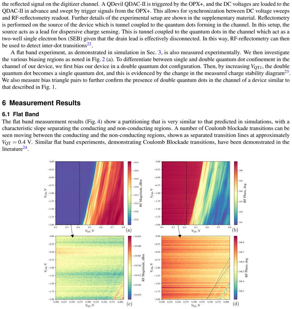
- [Sec. 6.1 and Introduction] The title and Introduction claim 'full electrical control over the location of the quantum dots, either underneath or between the gate electrodes' and 'confinement inversion'. However, the transport measurements in Sec. 6 do not directly determine where the dots are located relative to the gates. In Sec. 6.1, the assignment of the double-dot region is explicitly made 'by comparing with the simulation results in Fig. 2(a)' rather than by an experimental observable. Flat-band sweeps, charge stability diagrams, and bias triangles demonstrate the number of dots and their coupling, but not whether the dots sit under QT1 or between QT0/QT1 and QT1/QT2. Thus the central spatial prediction is not experimentally verified; it is an interpretation of the model. This gap should be stated explicitly and the abstract's 'verification of all model predictions' should be softened accordingly.
- [Appendix A] The calibration procedure yields 58 valid parameter sets from 9702 combinations, with the final choice based on matching a single Coulomb-diamond lever arm of the minimum-size transistor. The other 57 valid sets are not used to test the robustness of the QDA predictions. Since the model parameters (nsd, EWg, EWbg, nbg, spacer permittivity) are transferred to the five-gate array without re-fitting, equally good calibrations of the test transistor could yield different flat-band boundaries, different dot locations, or quantitatively different double-dot lever arms. The paper should show, for the ensemble of valid parameter sets, the spread in the predicted flat-band classification boundaries and in the double-dot lever arm, and confirm that the between-gate double-dot regime persists. Without this, the experimental agreement with one selected parameter set does not establish the predictive power claimed.
- [Sec. 2 (model assumptions)] The bullet list states that mechanical stress in the silicon channel is neglected and that this 'can introduce a noticeable offset between the biasing voltages predicted by simulation and those used in the experiment.' The same section notes that charge disorder at interfaces is expected. These effects are not merely third-order: the flat-band boundaries in Fig. 2(a) and the dot-location classification in Tab. 3 depend on precise band-edge alignment between gate and inter-gate regions. The authors should estimate the expected voltage shifts from stress and disorder and show whether the between-gate double-dot regime survives such shifts, or explicitly limit their predictions to the disorder-free idealization.
- [Abstract and Conclusions] The phrase 'experimental verification of all model predictions' (Abstract, restated in Conclusions) overstates the evidence. The quantitative verification is limited to one lever arm (Sec. 4: 0.261 eV/V compared with 0.2701 eV/V), while the flat-band partitioning and charge stability diagrams are qualitative comparisons. The spatial dot-location predictions are not directly verified at all. The abstract and conclusions should be revised to describe which predictions are quantitatively confirmed, which are qualitatively supported, and which remain simulation-based.
minor comments (5)
- [Table 1] The voltage definitions use primed and unprimed symbols (for example, V'_QR0 versus V_QR0) without an explicit statement that unprimed values are referenced to the source, although this is implied in the text. Please define this convention in the table caption.
- [Sec. 4] The term 'leverarm' is used as a single word; standard usage is 'lever arm', and this should be made consistent throughout the text.
- [Fig. 5] The caption states that measurements are shown for three values of VQT1 (0.33 V, 0.34 V, 0.35 V), but the panels (a)-(f) do not indicate which VQT1 value corresponds to which panel. Adding the value in each panel or in the caption will improve readability.
- [Sec. 4] The lever arm comparison of 0.261 eV/V with 0.2701 eV/V is stated to rely on 'supplementary materials' for the Coulomb diamond measurement and extraction method. It would be helpful to reference the specific appendix or figure where this is shown, as the appendices do not currently display the extraction.
- [Introduction] Reference [29] (arXiv:1202.6681) is cited for the lever arm extraction method; please verify that the published version is cited and that the method is briefly described in the text.
Circularity Check
No circularity: the QDA predictions are generated by a model calibrated on a separate minimum-size transistor and checked against independent experimental data.
full rationale
The central derivation chain is not circular. The QTCAD model is calibrated in Appendix A on a minimum-size 22 nm FD-SOI transistor, where the parameter filter requires E_min^C < E_F < E_max^C and the final parameter set is selected by matching a single measured Coulomb diamond (lever arm ≈0.8 eV/V; simulated ≈0.83 eV/V). These calibration targets do not include any of the five-gate QDA data. The QDA flat-band classification, dot locations under/between gates, and detuning lever arms are then computed by solving Poisson–Schrödinger equations with the transferred parameters; they are not fitted to the QDA measurements. The experimental results quoted as verification—flat-band slope, charge-stability transitions that change with VQT1, bias-triangle pairs, and the measured lever arm of ≈0.2701 eV/V against the simulated ≈0.261 eV/V—are independent of the calibration fit. The fact that the transport measurements cannot directly localize dots under versus between gates is a verifiability/correctness limitation, not a circular reduction. The only overlapping-author citation (ref. 18, prior QTCAD work) is used as general modeling support and is not load-bearing for the confinement-inversion claim; no uniqueness theorem or ansatz is imported from it. Therefore no step reduces by construction to its own inputs.
Assumptions & free parameters
free parameters (5)
- nsd =
not stated
- EWg =
not stated
- EWbg =
not stated
- nbg =
not stated
- foamed spacer dielectric constant =
2.7
assumptions (7)
- domain assumption Polysilicon gates behave as equipotential conductors at cryogenic temperatures
- domain assumption Spacers are perfect insulators with fixed dielectric constants
- domain assumption Doping in source and drain is uniform
- domain assumption Frozen boundary condition at the bottom of the buried oxide
- domain assumption Mechanical stress in the silicon channel is negligible
- domain assumption Calibration transfers from a minimum-size single-gate transistor to the five-gate QDA
- domain assumption Classical transport is forbidden in the dot region and sequential tunneling describes current
Cite this review
Pith. "Pith review of Common-Mode Control and Confinement Inversion of Electrostatically Defined Quantum Dots in a Commercial CMOS Process." pith.science (2026). https://pith.science/paper/IJGZOF6S
@misc{pith2026241208302,
  author       = {Pith},
  title        = {Pith review of: Common-Mode Control and Confinement Inversion of Electrostatically Defined Quantum Dots in a Commercial CMOS Process},
  year         = {2026},
  howpublished = {\url{https://pith.science/paper/IJGZOF6S}},
  note         = {Machine review of arXiv:2412.08302}
}
read the original abstract
Confining electrons or holes in quantum dots formed in the channel of industry-standard fully depleted silicon-on-insulator CMOS structures is a promising approach to scalable qubit architectures. In this article, we present our results on a calibrated model of a commercial nanostructure using the simulation tool Quantum TCAD, along with our experimental verification of all model predictions. We demonstrate here that quantum dots can be formed in the device channel by applying a combination of a common-mode voltage to the source and drain and a back gate voltage. Moreover, in this approach, the amount of quantum dots can be controlled and modified. Also, we report our results on an effective detuning of the energy levels in the quantum dots by varying the barrier gate voltages. Given the need and importance of scaling to larger numbers of qubits, we demonstrate here the feasibility of simulating and improving the design of quantum dot devices before their fabrication based on a commercial process.
Figures


Figures from the paper (4 more)


Reference graph
Works this paper leans on
-
[1]
Chatterjee, A. et al. Semiconductor Qubits In Practice. Nat. Rev. Phys. 3, 157–177, DOI: 10.1038/s42254-021-00283-9 (2021)
-
[2]
Burkard, G., Ladd, T. D., Pan, A., Nichol, J. M. & Petta, J. R. Semiconductor spin qubits. Rev. Mod. Phys. 95, 025003, DOI: 10.1103/RevModPhys.95.025003 (2023)
-
[3]
Vahapoglu, E. et al. Coherent control of electron spin qubits in silicon using a global field. npj Quantum Inf. 8, 126, DOI: 10.1038/s41534-022-00645-w (2022)
-
[4]
Ong, S. et al. 22nm FD-SOI Technology with Back-biasing Capability Offers Excellent Performance for Enabling Efficient, Ultra-low Power Analog and RF/Millimeter-Wave Designs. 323–326, DOI: 10.1109/RFIC.2019.8701768 (2019)
arXiv 2019
-
[5]
Seidler, I. et al. Conveyor-mode single-electron shuttling in Si/SiGe for a scalable quantum computing architecture. npj Quantum Inf. 8, 1–7, DOI: 10.1038/s41534-022-00615-2 (2022)
-
[6]
West, A. et al. Gate-based single-shot readout of spins in silicon. Nat. Nanotechnol. 14, 437–441, DOI: 10.1038/ s41565-019-0400-7 (2019)
work page 2019
-
[7]
Ciriano-Tejel, V . N.et al. Spin readout of a CMOS quantum dot by gate reflectometry and spin-dependent tunnelling. PRX Quantum 2, 010353, DOI: 10.1103/PRXQuantum.2.010353 (2021)
-
[8]
Piot, N. et al. A single hole spin with enhanced coherence in natural silicon. Nat. Nanotechnol. 17, 1072–1077, DOI: 10.1038/s41565-022-01196-z (2022). 10/17
Show all 34 references
-
[9]
& Graziano, M
Costa, D., Simoni, M., Piccinini, G. & Graziano, M. Advances in Modeling of Noisy Quantum Computers: Spin Qubits in Semiconductor Quantum Dots. IEEE Access 11, 98875–98913, DOI: 10.1109/ACCESS.2023.3312559 (2023)
2023
-
[10]
The path to scalable quantum computing with silicon spin qubits
Vinet, M. The path to scalable quantum computing with silicon spin qubits. Nat. Nanotechnol. 16, 1294–1296, DOI: https://doi.org/10.1038/s41565-021-01037-5 (2021)
2021 doi
-
[11]
& Zhao, Y
Wu, Q., Li, Y . & Zhao, Y . The Evolution of Photolithography Technology, Process Standards, and Future Outlook. In 2020 IEEE 15th International Conference on Solid-State & Integrated Circuit Technology (ICSICT) , 1–5, DOI: 10.1109/ICSICT49897.2020.9278164 (2020)
2020
-
[12]
Hou, Y . & Wu, Q. Optical Proximity Correction, Methodology and Limitations. In2021 China Semiconductor Technology International Conference (CSTIC), 1–5, DOI: 10.1109/CSTIC52283.2021.9461507 (2021)
2021
-
[13]
Y ., Lee, S., Yang, J
Park, S. Y ., Lee, S., Yang, J. & Kang, M. S. Patterning Quantum Dots via Photolithography: A Review.Adv. Mater. 35, 2300546, DOI: 10.1002/adma.202300546 (2023)
2023 doi
-
[14]
& Enz, C
Beckers, A., Jazaeri, F. & Enz, C. Cryogenic MOS Transistor Model. IEEE Transactions on Electron Devices 65, 3617–3625, DOI: 10.1109/TED.2018.2854701 (2018)
2018
-
[15]
Gao, X. et al. Quantum computer aided design simulation and optimization of semiconductor quantum dots. J. Appl. Phys. 114, 164302, DOI: 10.1063/1.4825209 (2013)
2013 doi
-
[16]
QTCAD: A Computer-Aided Design Tool for Quantum-Technology Hardware, Nanoacademic Technologies Inc. (2022)
2022
-
[17]
Beaudoin, F. et al. Robust technology computer-aided design of gated quantum dots at cryogenic temperature. Appl. Phys. Lett. 120, 264001, DOI: 10.1063/5.0097202 (2022)
2022 doi
-
[18]
Kriekouki, I. et al. Interpretation of 28 nm FD-SOI quantum dot transport data taken at 1.4 K using 3D quantum TCAD simulations. Solid-State Electron. 194, 108355, DOI: 10.1016/j.sse.2022.108355 (2022)
2022
-
[19]
Introducing Technology Computer-aided Design (TCAD): Fundamentals, Simulations and Applications (Pan Stanford Publishing Pte
Maiti, C. Introducing Technology Computer-aided Design (TCAD): Fundamentals, Simulations and Applications (Pan Stanford Publishing Pte. Limited, 2017)
2017
-
[20]
Advanced Semiconductor Fundamentals
Pierret, R. Advanced Semiconductor Fundamentals. Modular series on solid state devices (Prentice Hall, 2003)
2003
-
[21]
Quantum Machines, www.quantum-machines.co
-
[22]
Vigneau, F. et al. Probing quantum devices with radio-frequency reflectometry. Appl. Phys. Rev. 10, 021305, DOI: 10.1063/5.0088229 (2023)
2023 doi
-
[23]
Van Der Wiel, W. G.et al. Electron transport through double quantum dots. Rev. Mod. Phys. 75, 1–22, DOI: 10.1103/ RevModPhys.75.1 (2002)
2002
-
[24]
& Oda, S
Yamada, K., Kodera, T., Kambara, T. & Oda, S. Fabrication and characterization of p-channel Si double quantum dots. Appl. Phys. Lett. 105, 113110, DOI: 10.1063/1.4896142 (2014)
2014 doi
-
[25]
Vinet, M. et al. Material and integration challenges for large scale Si quantum computing. In 2021 IEEE International Electron Devices Meeting (IEDM), 14.2.1–14.2.4, DOI: 10.1109/IEDM19574.2021.9720708 (2021). ISSN: 2156-017X
2021
-
[26]
& Niquet, Y .-M
Martinez, B. & Niquet, Y .-M. Variability of Electron and Hole Spin Qubits Due to Interface Roughness and Charge Traps. Phys. Rev. Appl. 17, 024022, DOI: 10.1103/PhysRevApplied.17.024022 (2022)
2022 doi
-
[27]
Chorley, S. J. et al. Measuring the complex admittance of a carbon nanotube double quantum dot. Phys. Rev. Lett. 108, 036802, DOI: 10.1103/PhysRevLett.108.036802 (2012)
2012 doi
-
[28]
Stehlik, J. et al. Fast Charge Sensing of a Cavity-Coupled Double Quantum Dot Using a Josephson Parametric Amplifier. Phys. Rev. Appl. 4, 014018, DOI: 10.1103/PhysRevApplied.4.014018 (2015)
2015 doi
-
[29]
& Yacoby, A
Venkatachalam, V ., Hart, S., Pfeiffer, L., West, K. & Yacoby, A. Local Thermometry of Neutral Modes on the Quantum Hall Edge, DOI: 10.48550/arXiv.1202.6681 (2012). ArXiv:1202.6681. 11/17 A QTCAD Model Calibration As discussed in the main text, the QTCAD model requires calibra...
-
[30]
Solve the Poisson equation with QTCAD at the given set of parameters
-
[31]
Select three line cuts in the Silicon channel (at height 0 .1 nm, 3.0 nm and 5.9 nm from the top of the channel)
-
[32]
Define the maximal, Emax C , and minimal, Emin C , values of the conduction band edge (the minimal value is defined under the gate not including the source and drain regions)
-
[33]
Define the Fermi level, EF, under the source and drain (since the source/drain voltages are set by the shifting of the Fermi levels under the source and the drain)
-
[34]
The given algorithm filtered 58 valid sets of parameters of the 9702 tested
The set of parameters is considered to be valid if Emin C < EF < Emax C . The given algorithm filtered 58 valid sets of parameters of the 9702 tested. An example of a valid 1D line cut of the conduction band is shown in Figure A.1 (d). The conduction band edge that forms the d...
Reviewed August 11, 2026 · model on record in the stance chip above.
Discussion (0). Continue with ORCID to comment.