Probing PbTe-Pb nanowire devices with radio-frequency reflectometry
Reviewed by Pith T0 review T1 audit T2 compute T3 formal T4 kernel 2026-06-28 05:12 UTCgrok-4.3pith:UEYMMOVArecord.jsonopen to challenge →
The pith
Radio-frequency reflectometry works on PbTe-Pb nanowire devices even under magnetic fields needed for zero-energy modes.
A machine-rendered reading of the paper's core claim, the machinery that carries it, and where it could break.
Core claim
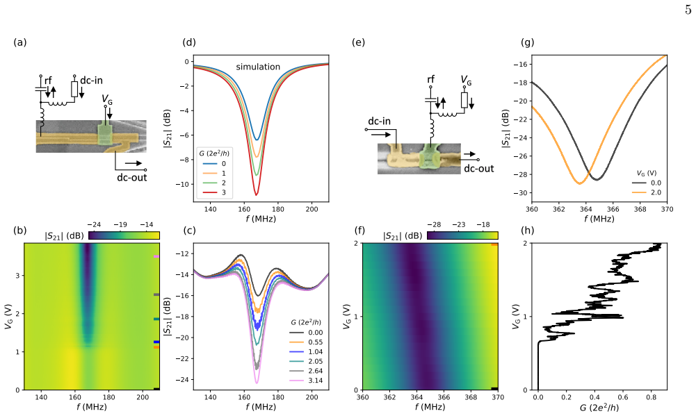
Implementation of rf reflectometry on PbTe-Pb nanowire devices demonstrates compatibility for resistive and capacitive sensing, with dielectric loss from the CdTe substrate quantitatively characterized, and feasibility verified under finite magnetic fields where zero-energy modes can emerge.
What carries the argument
Radio-frequency reflectometry applied for sensing changes in the nanowire devices, including resistive and capacitive components.
If this is right
- Fast control and readout of PbTe quantum devices is established.
- The technique remains viable in magnetic fields where zero-energy modes may appear.
- Applications in topological quantum computation using these nanowires are supported.
Where Pith is reading between the lines
- Similar rf methods could be applied to other nanowire platforms for Majorana research.
- Substrate loss characterization may guide material choices to improve signal quality in related devices.
- Real-time monitoring of mode formation might become feasible with this fast technique.
Load-bearing premise
Dielectric losses from the CdTe substrate can be quantitatively characterized and do not prevent reliable detection or control of zero-energy modes under applied magnetic fields.
What would settle it
A measurement showing that rf reflectometry signals degrade or become unusable under the magnetic fields required for zero-energy mode emergence would falsify the feasibility claim.
Figures





read the original abstract
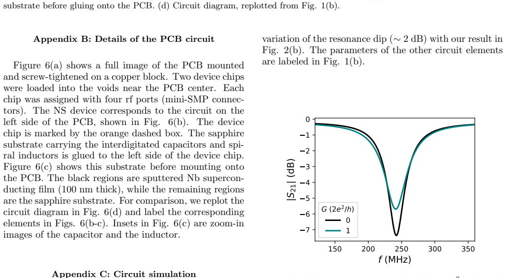
We report the implementation of radio-frequency (rf) reflectometry on selective-area-grown PbTe-Pb nanowire devices on a CdTe substrate. These nanowires are predicted to host Majorana zero modes. We demonstrate the compatibility of the rf technique, including both resistive and capacitive sensing, with these nanowires. The effect of dielectric loss from the CdTe substrate is quantitatively characterized. Furthermore, the feasibility of rf reflectometry is verified under finite magnetic fields where zero-energy modes can emerge. Our results establish the fast control of PbTe quantum devices, paving the way for their applications in topological quantum computation.
Editorial analysis
A structured set of objections, weighed in public.
Referee Report
Summary. The manuscript reports the implementation of radio-frequency reflectometry on selective-area-grown PbTe-Pb nanowire devices fabricated on a CdTe substrate. It claims to demonstrate compatibility of the rf technique for both resistive and capacitive sensing, to quantitatively characterize the dielectric loss arising from the CdTe substrate, and to verify that the method remains feasible under finite magnetic fields where zero-energy modes are expected to emerge.
Significance. If the experimental results are robust, the work would establish fast rf-based control of PbTe quantum devices and thereby open a route toward their use in topological quantum computation. The quantitative treatment of substrate dielectric losses is a potentially useful contribution for device design in this material system.
minor comments (1)
- The abstract states that dielectric loss is 'quantitatively characterized' and that feasibility is 'verified' under magnetic field, yet no numerical values, error bars, or figure references are supplied in the provided text; the full manuscript must be examined to assess whether the data support these claims.
Simulated Author's Rebuttal
We thank the referee for reviewing our manuscript and for the accurate summary provided. We appreciate the recognition of the potential significance for topological quantum computation applications. No specific major comments are listed in the report, so we have no individual points to address. We remain available to supply additional data or clarifications that might resolve the uncertainty in the recommendation.
Circularity Check
No significant circularity in experimental demonstration
full rationale
This is a purely experimental paper reporting the implementation and characterization of rf reflectometry on PbTe-Pb nanowire devices. The abstract and claims describe direct measurements of compatibility, dielectric losses, and performance under magnetic fields, with no derivations, equations, fitted predictions, or self-referential steps. All load-bearing results are observational and externally verifiable through the reported experiments rather than reducing to inputs by construction or self-citation chains. The work is self-contained against external benchmarks with no mathematical circularity present.
Axiom & Free-Parameter Ledger
axioms (1)
- domain assumption PbTe-Pb nanowires on CdTe substrates are predicted to host Majorana zero modes under applied magnetic fields
Reference graph
Works this paper leans on
-
[1]
Z. Cao, D. E. Liu, W.-X. He, X. Liu, K. He, and H. Zhang, Numerical study of PbTe-Pb hybrid nanowires for engineering Majorana zero modes, Phys. Rev. B105, 085424 (2022)
2022
-
[2]
Jiang, S
Y. Jiang, S. Yang, L. Li, W. Song, W. Miao, B. Tong, Z. Geng, Y. Gao, R. Li, F. Chen, Q. Zhang, F. Meng, L. Gu, K. Zhu, Y. Zang, R. Shang, Z. Cao, X. Feng, Q.-K. Xue, D. E. Liu, H. Zhang, and K. He, Selective area epi- taxy of PbTe-Pb hybrid nanowires on a lattice-matched substrate, Phys. Rev. Materials6, 034205 (2022)
2022
-
[3]
J. Jung, S. G. Schellingerhout, M. F. Ritter, S. C. ten Kate, O. A. van der Molen, S. de Loijer, M. A. Verheijen, H. Riel, F. Nichele, and E. P. Bakkers, Selective area growth of PbTe nanowire networks on InP, Advanced Functional Materials32, 2208974 (2022)
2022
-
[4]
R. M. Lutchyn, J. D. Sau, and S. Das Sarma, Ma- jorana fermions and a topological phase transition in semiconductor-superconductor heterostructures, Phys. Rev. Lett.105, 077001 (2010)
2010
-
[5]
Y. Oreg, G. Refael, and F. von Oppen, Helical liquids and Majorana bound states in quantum wires, Phys. Rev. Lett.105, 177002 (2010)
2010
-
[6]
Nayak, S
C. Nayak, S. H. Simon, A. Stern, M. Freedman, and S. Das Sarma, Non-Abelian anyons and topological quan- tum computation, Rev. Mod. Phys.80, 1083 (2008)
2008
-
[7]
Z. Geng, Z. Zhang, F. Chen, S. Yang, Y. Jiang, Y. Gao, B. Tong, W. Song, W. Miao, R. Li, Y. Wang, Q. Zhang, F. Meng, L. Gu, K. Zhu, Y. Zang, L. Li, R. Shang, X. Feng, Q.-K. Xue, K. He, and H. Zhang, Observation of Aharonov-Bohm effect in PbTe nanowire networks, Phys. Rev. B105, L241112 (2022)
2022
-
[8]
S. C. ten Kate, M. F. Ritter, A. Fuhrer, J. Jung, S. G. Schellingerhout, E. P. A. M. Bakkers, H. Riel, and F. Nichele, Small charging energies and g-factor anisotropy in PbTe quantum dots, Nano Letters22, 7049 (2022). 9
2022
-
[9]
Zhang, W
Z. Zhang, W. Song, Y. Gao, Y. Wang, Z. Yu, S. Yang, Y. Jiang, W. Miao, R. Li, F. Chen, Z. Geng, Q. Zhang, F. Meng, T. Lin, L. Gu, K. Zhu, Y. Zang, L. Li, R. Shang, X. Feng, Q.-K. Xue, K. He, and H. Zhang, Proximity effect in PbTe-Pb hybrid nanowire Josephson junctions, Phys. Rev. Mater.7, 086201 (2023)
2023
-
[10]
W. Song, Y. Wang, W. Miao, Z. Yu, Y. Gao, R. Li, S. Yang, F. Chen, Z. Geng, Z. Zhang, S. Zhang, Y. Zang, Z. Cao, D. E. Liu, R. Shang, X. Feng, L. Li, Q.-K. Xue, K. He, and H. Zhang, Conductance quantization in PbTe nanowires, Phys. Rev. B108, 045426 (2023)
2023
-
[11]
Y. Gao, W. Song, S. Yang, Z. Yu, R. Li, W. Miao, Y. Wang, F. Chen, Z. Geng, L. Yang, Z. Xia, X. Feng, Y. Zang, L. Li, R. Shang, Q.-K. Xue, K. He, and H. Zhang, Hard superconducting gap in PbTe nanowires, Chinese Physics Letters41, 038502 (2024)
2024
-
[12]
Y. Wang, F. Chen, W. Song, Z. Geng, Z. Yu, L. Yang, Y. Gao, R. Li, S. Yang, W. Miao, W. Xu, Z. Wang, Z. Xia, H.-D. Song, X. Feng, T. Wang, Y. Zang, L. Li, R. Shang, Q. Xue, K. He, and H. Zhang, Ballistic PbTe nanowire devices, Nano Letters23, 11137 (2023)
2023
-
[13]
R. Li, W. Song, W. Miao, Z. Yu, Z. Wang, S. Yang, Y. Gao, Y. Wang, F. Chen, Z. Geng, L. Yang, J. Xu, X. Feng, T. Wang, Y. Zang, L. Li, R. Shang, Q. Xue, K. He, and H. Zhang, Selective-area-grown PbTe-Pb pla- nar Josephson junctions for quantum devices, Nano Let- ters24, 4658 (2024)
2024
-
[14]
Gupta, V
M. Gupta, V. Khade, C. Riggert, L. Shani, G. Menning, P. J. H. Lueb, J. Jung, R. M´ elin, E. P. A. M. Bakkers, and V. S. Pribiag, Evidence forπ-shifted cooper quartets and few-mode transport in pbte nanowire three-terminal josephson junctions, Nano Letters24, 13903 (2024)
2024
-
[15]
Z. Geng, F. Chen, Y. Gao, L. Yang, Y. Wang, S. Yang, S. Zhang, Z. Li, W. Song, J. Xu,et al., Enhanced super- conductivity in PbTe-In hybrids, Phys. Rev. Mater.9, 084802 (2025)
2025
-
[16]
Y. Gao, W. Song, Z. Yu, S. Yang, Y. Wang, R. Li, F. Chen, Z. Geng, L. Yang, J. Xu, Z. Wang, Z. Li, S. Zhang, X. Feng, T. Wang, Y. Zang, L. Li, R. Shang, Q.-K. Xue, K. He, and H. Zhang, SQUID oscillations in PbTe nanowire networks, Phys. Rev. B110, 045405 (2024)
2024
-
[17]
Z. Li, W. Song, S. Zhang, Y. Wang, Z. Wang, Z. Yu, R. Li, Z. Yan, J. Xu, Y. Gao, S. Yang, L. Yang, X. Feng, T. Wang, Y. Zang, L. Li, R. Shang, Q.-K. Xue, K. He, and H. Zhang, Anisotropy of PbTe nanowires with and without a superconductor, Phys. Rev. B111, 195416 (2025)
2025
-
[18]
Y. Wang, L. Yang, W. Song, L. Chen, Z. Yu, X. He, Z. Yan, J. Xu, R. Li, W. Wang,et al., Presence ver- sus absence of charging energies in PbTe quantum dots, Phys. Rev. B (2026)
2026
-
[19]
Y. Wang, W. Song, Z. Cao, Z. Yu, S. Yang, Z. Li, Y. Gao, R. Li, F. Chen, Z. Geng, L. Yang, J. Xu, Z. Wang, S. Zhang, X. Feng, T. Wang, Y. Zang, L. Li, R. Shang, Q.-K. Xue, D. E. Liu, K. He, and H. Zhang, Gate- tunable subband degeneracy in semiconductor nanowires, Proceedings of the National Academy of Sciences121, e2406884121 (2024)
2024
-
[20]
W. Song, Z. Yu, Y. Wang, Y. Gao, Z. Li, S. Yang, S. Zhang, Z. Geng, R. Li, Z. Wang,et al., Reducing dis- order in PbTe nanowires for Majorana research, Nano Letters25, 2350 (2025)
2025
-
[21]
Y. Gao, W. Song, Y. Wang, Z. Geng, Z. Cao, Z. Yu, S. Yang, J. Xu, F. Chen, Z. Li,et al., Quantized An- dreev conductance in semiconductor nanowires, Phys. Rev. Appl.23, L061004 (2025)
2025
-
[22]
Zhang, W
S. Zhang, W. Song, Z. Li, Z. Yu, R. Li, Y. Wang, Z. Yan, J. Xu, Z. Wang, Y. Gao, S. Yang, L. Yang, X. Feng, T. Wang, Y. Zang, L. Li, R. Shang, Q.-K. Xue, K. He, and H. Zhang, Strong enhancement of g-factor in PbTe–Pb hybrid nanowires, Nano Letters26, 4739 (2026)
2026
-
[23]
Liet al., Gate-tunable superconductor-semiconductor coupling and its impact on zero-energy modes in PbTe- Pb nanowires, (to be appeared) (2026)
R. Liet al., Gate-tunable superconductor-semiconductor coupling and its impact on zero-energy modes in PbTe- Pb nanowires, (to be appeared) (2026)
2026
-
[24]
Plugge, A
S. Plugge, A. Rasmussen, R. Egger, and K. Flensberg, Majorana box qubits, New Journal of Physics19, 012001 (2017)
2017
-
[25]
Karzig, C
T. Karzig, C. Knapp, R. M. Lutchyn, P. Bonder- son, M. B. Hastings, C. Nayak, J. Alicea, K. Flens- berg, S. Plugge, Y. Oreg, C. M. Marcus, and M. H. Freedman, Scalable designs for quasiparticle-poisoning- protected topological quantum computation with Majo- rana zero modes, Phys. Rev. B95, 235305 (2017)
2017
-
[26]
D. J. Reilly, C. M. Marcus, M. P. Hanson, and A. C. Gossard, Fast single-charge sensing with a rf quantum point contact, Applied Physics Letters91, 162101 (2007)
2007
-
[27]
M. D. Schroer, M. Jung, K. D. Petersson, and J. R. Petta, Radio frequency charge parity meter, Phys. Rev. Lett. 109, 166804 (2012)
2012
-
[28]
N. Ares, F. J. Schupp, A. Mavalankar, G. Rogers, J. Grif- fiths, G. A. C. Jones, I. Farrer, D. A. Ritchie, C. G. Smith, A. Cottet, G. A. D. Briggs, and E. A. Laird, Sen- sitive radio-frequency measurements of a quantum dot by tuning to perfect impedance matching, Phys. Rev. Appl. 5, 034011 (2016)
2016
-
[29]
Razmadze, D
D. Razmadze, D. Sabonis, F. K. Malinowski, G. C. M´ enard, S. Pauka, H. Nguyen, D. M. van Zanten, E. C. O′Farrell, J. Suter, P. Krogstrup, F. Kuemmeth, and C. M. Marcus, Radio-Frequency methods for Majorana- based quantum devices: Fast charge sensing and phase- diagram mapping, Phys. Rev. Appl.11, 064011 (2019)
2019
-
[30]
D. M. T. van Zanten, D. Sabonis, J. Suter, J. I. V¨ ayrynen, T. Karzig, D. I. Pikulin, E. C. T. O’Farrell, D. Razmadze, K. D. Petersson, P. Krogstrup, and C. M. Marcus, Photon-assisted tunnelling of zero modes in a Majorana wire, Nature Physics16, 663 (2020)
2020
-
[31]
F. K. Malinowski, L. Han, D. de Jong, J.-Y. Wang, C. G. Prosko, G. Badawy, S. Gazibegovic, Y. Liu, P. Krogstrup, E. P. Bakkers, L. P. Kouwenhoven, and J. V. Koski, Radio-FrequencyC-Vmeasurements with subattofarad sensitivity, Phys. Rev. Appl.18, 024032 (2022)
2022
-
[32]
Vigneau, F
F. Vigneau, F. Fedele, A. Chatterjee, D. Reilly, F. Kuem- meth, M. F. Gonzalez-Zalba, E. Laird, and N. Ares, Probing quantum devices with radio-frequency reflectom- etry, Applied Physics Reviews10, 021305 (2023)
2023
-
[33]
Tanget al., Zenodo,https://doi.org/10.5281/ zenodo.20592971(2026)
X.-Y. Tanget al., Zenodo,https://doi.org/10.5281/ zenodo.20592971(2026)
2026
discussion (0)
Sign in with ORCID, Apple, or X to comment. Anyone can read and Pith papers without signing in.