Organic Semiconductor Alignment via Confinement in Vapor-Guided Droplets
Pith reviewed 2026-06-26 02:20 UTC · model grok-4.3
The pith
Vapor-guided microliter droplets harness internal flows to align organic semiconductor nanowires, producing films with 40% higher transistor saturation current than spin-coated controls.
A machine-rendered reading of the paper's core claim, the machinery that carries it, and where it could break.
Core claim
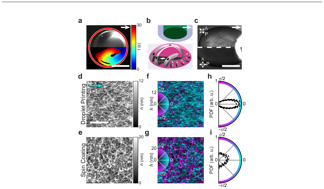
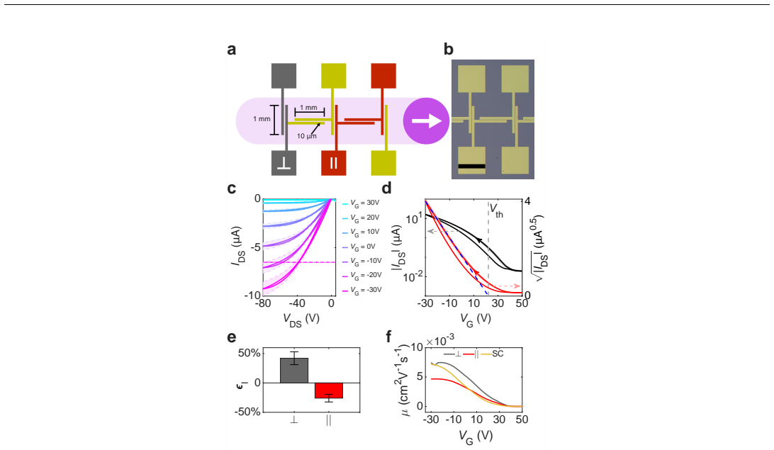
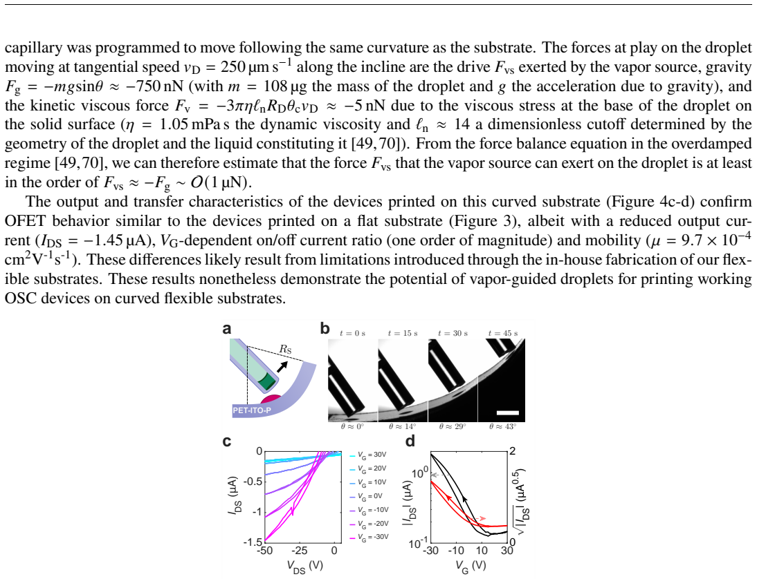
Flows developing within the intrinsically confined volume of microliter vapor-guided droplets align organic semiconducting nanowires prior to deposition, yielding films with pronounced directional order. Organic field-effect transistors fabricated with this approach exhibit approximately 40% enhancement in saturation current relative to spin-coated controls. The contactless and compact nature of the method enables deposition and alignment on curved and flexible surfaces.
What carries the argument
Internal flows induced by vapor-guided confinement within the volume of microliter droplets, which align nanowires before deposition.
If this is right
- Films display pronounced directional order from the alignment of nanowires during droplet motion.
- Transistors show approximately 40% higher saturation current than spin-coated controls.
- Deposition and alignment occur on curved and flexible surfaces without direct contact.
- The technique supplies a scalable framework for confinement-induced alignment of functional soft materials.
- Integration into existing additive manufacturing platforms becomes feasible for flexible electronics.
Where Pith is reading between the lines
- Adjusting droplet speed or vapor source position could regionally tune alignment strength within a single film.
- The confinement mechanism may align other rod-like particles such as carbon nanotubes if similar flows develop.
- Pairing vapor guidance with inkjet nozzles might combine alignment with precise patterning in one step.
- Gains on flexible substrates imply better charge transport stability under repeated bending in wearable devices.
Load-bearing premise
The directional order and current enhancement arise specifically from the internal flows induced by vapor-guided confinement rather than from solvent evaporation rate, substrate interactions, or nanowire concentration.
What would settle it
A control deposition using identical droplet volumes, nanowire concentrations, and evaporation conditions but without vapor guidance produces films with no measurable directional order or current enhancement.
Figures

read the original abstract
Organic semiconductors are lightweight, solution-processable materials with strong potential for printed and flexible electronics, from deformable displays to wearable sensors. Despite significant advances in materials synthesis and manufacturing, controlling molecular and mesoscale alignment during deposition remains a central challenge, as film morphology critically governs charge transport and device performance. Here, we demonstrate that flows developing within the intrinsically confined volume of microliter vapor-guided droplets can be harnessed to produce highly aligned organic semiconductor films. As droplets move in response to an external vapor source, internal flows align organic semiconducting nanowires within the droplet prior to deposition, yielding films with pronounced directional order. Organic field-effect transistors fabricated with this approach exhibit approximately 40% enhancement in saturation current relative to spin-coated controls. Beyond improved device performance, the contactless and compact nature of our method enables the deposition and alignment of organic semiconductors on curved and flexible surfaces. More broadly, vapor-guided droplets offer a scalable framework for the confinement-induced alignment of functional soft materials, with potential for integration into existing additive manufacturing platforms for flexible electronics and beyond.
Editorial analysis
A structured set of objections, weighed in public.
Referee Report
Summary. The manuscript claims that flows within the confined volume of moving microliter vapor-guided droplets can be used to align organic semiconducting nanowires prior to deposition, producing films with pronounced directional order. OFETs fabricated from these films exhibit ~40% higher saturation current than spin-coated controls; the method is also presented as contactless and suitable for curved/flexible substrates.
Significance. If the reported alignment and performance gain can be shown to arise specifically from the vapor-induced internal flows rather than from generic droplet deposition or evaporation effects, the approach would offer a scalable, contactless route to aligned organic semiconductor films on non-planar surfaces, with potential integration into additive manufacturing for flexible electronics.
major comments (2)
- [Abstract] Abstract: the central performance claim (~40% saturation-current enhancement) is presented without error bars, sample size, or statistical details, and the comparison is made only against spin-coated controls; this prevents verification that the data support the stated mechanism of vapor-guided confinement.
- [Abstract] Abstract (and implied experimental sections): no static-droplet controls on the same substrate, no flow visualization (e.g., particle tracking), and no independent variation of evaporation rate while holding confinement fixed are described; without these, the attribution of directional order and current gain specifically to internal flows induced by vapor-guided confinement cannot be isolated from confounding variables such as solvent evaporation or nanowire concentration.
minor comments (1)
- [Abstract] Abstract: the term 'highly aligned' is used without a quantitative metric (e.g., order parameter or dichroic ratio) or description of the alignment quantification method.
Simulated Author's Rebuttal
We thank the referee for their constructive comments on our manuscript. We address each major comment point by point below and indicate where revisions have been made to the manuscript.
read point-by-point responses
-
Referee: [Abstract] Abstract: the central performance claim (~40% saturation-current enhancement) is presented without error bars, sample size, or statistical details, and the comparison is made only against spin-coated controls; this prevents verification that the data support the stated mechanism of vapor-guided confinement.
Authors: We agree that the abstract would be strengthened by explicit reference to the statistical details already present in the main text. We have revised the abstract to direct readers to Figure 4 and the associated supplementary statistical analysis, where the saturation current data are shown with error bars across multiple devices and the comparison to spin-coated controls is quantified. The directional order metric is likewise tied to the vapor-guided condition in the results section. revision: yes
-
Referee: [Abstract] Abstract (and implied experimental sections): no static-droplet controls on the same substrate, no flow visualization (e.g., particle tracking), and no independent variation of evaporation rate while holding confinement fixed are described; without these, the attribution of directional order and current gain specifically to internal flows induced by vapor-guided confinement cannot be isolated from confounding variables such as solvent evaporation or nanowire concentration.
Authors: We acknowledge the value of these additional controls for isolating the mechanism. In the revised manuscript we have added a dedicated paragraph describing static-droplet control experiments performed on identical substrates, which exhibit measurably lower alignment. Particle-tracking visualization of internal flows has also been incorporated into the supplementary information. Fully independent variation of evaporation rate at fixed confinement geometry remains experimentally difficult within the vapor-guiding framework; we have instead reported the effects of varying vapor-source distance (which modulates both flow and evaporation) and discuss the resulting trends in the text. revision: partial
Circularity Check
No circularity: purely experimental demonstration with no derivations or self-referential predictions
full rationale
The paper reports an experimental method for aligning organic semiconductor nanowires using vapor-guided droplets, with device performance compared to spin-coated controls. The abstract and described content contain no equations, fitted parameters, predictions derived from prior results, or self-citations that bear load on a derivation chain. All claims rest on direct fabrication, imaging, and electrical measurements rather than any reduction of outputs to inputs by construction. This matches the default expectation for non-circular experimental work.
Axiom & Free-Parameter Ledger
axioms (1)
- domain assumption Film morphology (molecular and mesoscale alignment) critically governs charge transport and device performance in organic semiconductors.
Reference graph
Works this paper leans on
-
[1]
D. F. Wilcock, Journal of the American Chemical Society 1946, 68, 4 691
1946
-
[2]
R. S. Myers, H. L. Clever, Journal of Chemical and Engineering Data 1969, 14, 2 161
1969
-
[3]
L. Xue, X. Yu, Y . Han, Colloids and Surfaces A: Physicochemical and Engineering Aspects 2011, 380, 1-3 334
2011
-
[4]
Machui, S
F. Machui, S. Langner, X. Zhu, S. Abbott, C. J. Brabec, Solar Energy Materials and Solar Cells 2012, 100 138
2012
-
[5]
E. T. Niles, J. D. Roehling, H. Y amagata, A. J. Wise, F. C. Spano, A. J. Moulé, J. K. Grey, The Journal of Physical Chemistry Letters 2012, 3, 2 259
2012
-
[6]
F. Dou, J. Li, H. Men, X. Zhang, Polymers 2020, 12, 4 786
2020
-
[7]
Nagamatsu, W
S. Nagamatsu, W. Takashima, K. Kaneto, Y . Y oshida, N. Tanigaki, K. Y ase, K. Omote, Macromolecules 2003, 36, 14 5252
2003
-
[8]
G. Pace, I. Bargigia, Y .- Y . Noh, C. Silva, M. Caironi,Nature Communications 2019, 10, 1 5226
2019
-
[9]
Samitsu, T
S. Samitsu, T. Shimomura, S. Heike, T. Hashizume, K. Ito, Macromolecules 2008, 41, 21 8000
2008
-
[10]
Q. Li, Y . T. Zhu, I. A. Kinloch, A. H. Windle, The Journal of Physical Chemistry B 2006, 110, 28 13926
2006
-
[11]
W . A. Memon, Y . Zhang, J. Zhang, Y . Y an, Y . Wang, Z. Wei,Macromolecular Rapid Communications 2022, 43, 14 2100931
2022
-
[12]
L. A. Kehrer, S. Winter, R. Fischer, C. Melzer, H. von Seggern, Synthetic metals 2012, 161, 23-24 2558
2012
-
[13]
N. Fata, S. Mishra, Y . Xue, Y . Wang, J. Hicks, A. Ural, Journal of Applied Physics 2020, 128, 12
2020
-
[14]
X. Ding, J. Liu, T. A. Harris, AIChE Journal 2016, 62, 7 2508
2016
-
[15]
Malinowski, I
R. Malinowski, I. P . Parkin, G. Volpe, Chemical Society Reviews 2020, 49, 22 7879
2020
-
[16]
J. Choi, C. Han, S. Cho, K. Kim, J. Ahn, D. Del Orbe, I. Cho, Z.-J. Zhao, Y . S. Oh, H. Hong, et al., Science Advances 2021, 7, 42 eabj0694
2021
-
[17]
Thapa, R
A. Thapa, R. Malinowski, M. O. Blunt, G. Volpe, J. Forth, Journal of Colloid and Interface Science 2025, 695 137665
2025
-
[18]
Wodlei, J
F. Wodlei, J. Sebilleau, J. Magnaudet, V . Pimienta, Nature Communications 2018, 9, 1 820
2018
-
[19]
D. A. Baumgartner, S. Shiri, S. Sinha, S. Karpitschka, N. J. Cira, Proceedings of the National Academy of Sciences 2022, 119, 19 e2120432119
2022
-
[20]
Forth, R
J. Forth, R. Malinowski, G. Volpe, Europhysics Letters 2026, 153, 5 57002
2026
-
[21]
Fonck, G
E. Fonck, G. G. Feigl, J. Fasel, D. Sage, M. Unser, D. A. Rüfenacht, N. Stergiopulos, Stroke 2009, 40, 7 2552
2009
-
[22]
Rezakhaniha, A
R. Rezakhaniha, A. Agianniotis, J. T. C. Schrauwen, A. Griffa, D. Sage, C. v. Bouten, F. Van De Vosse, M. Unser, N. Stergiopulos, Biomechanics and mMdeling in Mechanobiology 2012, 11 461
2012
-
[23]
Püspöki, M
Z. Püspöki, M. Storath, D. Sage, M. Unser, Focus on Bio-image Informatics 2016, 69–93
2016
-
[24]
Jähne, Spatio-temporal Image Processing: Theory and Scientific Applications , Springer, 1993
B. Jähne, Spatio-temporal Image Processing: Theory and Scientific Applications , Springer, 1993
1993
-
[25]
N. I. Fisher, Statistical Analysis of Circular Data , Cambridge University Press, 1993
1993
-
[26]
Lee, H.- Y
K. Lee, H.- Y . Kim, M. Lotya, J. N. Coleman, G.-T. Kim, G. S. Duesberg, Advanced Materials 2011, 23, 36 4178
2011
-
[27]
J. S. Kim, J. H. Lee, J. H. Park, C. Shim, M. Sim, K. Cho, Advanced Functional Materials 2011, 21, 3 480. 14 SUPPLEMENTARY MATERIALS Supplementary Materials Supplementary Figures a b λ (nm) 400 500 600 700 800 A 0 1 2 3 λ = 610 nm λ = 563 nm λ = 522 nm λ = 458 nm ta = 0 h ta = 2 h ta = 4 h ta = 24 h ta = 48 h ta = 168 h ta = 264 h ta (h) 0 100 200 300 A61...
2011
discussion (0)
Sign in with ORCID, Apple, or X to comment. Anyone can read and Pith papers without signing in.