Industrially Microfabricated Ion Trap with 1 eV Trap Depth
Pith reviewed 2026-05-24 12:03 UTC · model grok-4.3
The pith
Stacked 8-inch wafers produce 3D ion traps with 1 eV depth via MEMS fabrication.
A machine-rendered reading of the paper's core claim, the machinery that carries it, and where it could break.
Core claim
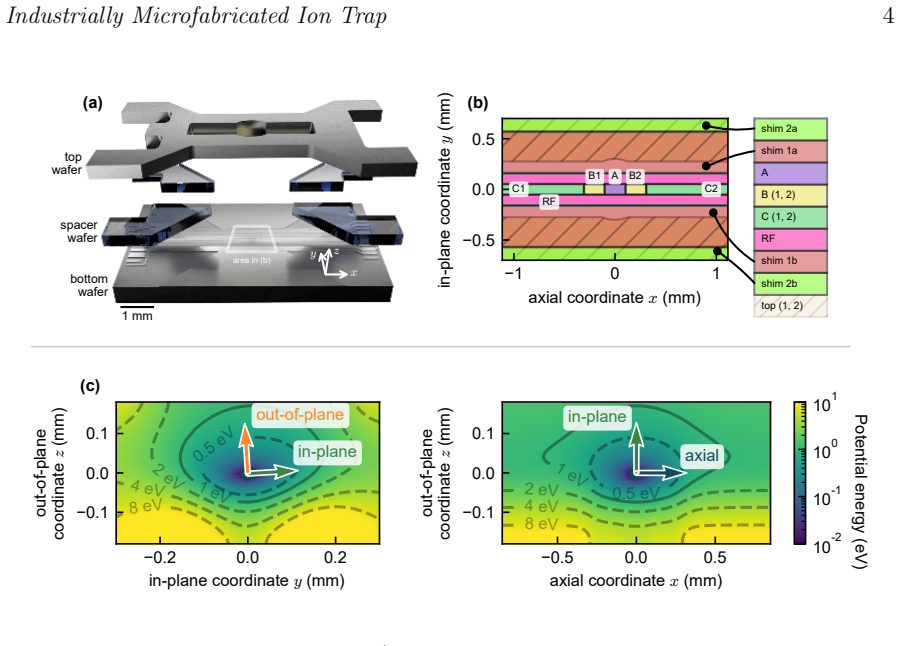
An ion trap fabricated on stacked 8-inch wafers in a large-scale MEMS microfabrication process forms a 3D electrode structure with electrodes patterned on opposing wafers bonded to a spacer. This design achieves a trap depth of 1 eV for a calcium-40 ion held at 200 micrometers from either electrode plane, with 2.5 micrometer standard deviation in alignment across the stack. The traps are characterized with mode frequencies spanning 0.6 to 3.8 MHz agreeing with simulations to within plus or minus 5 percent, stray electric fields evaluated across sites, and motional heating rates measured over ranges of trap frequencies and temperatures.
What carries the argument
The stacked wafer 3D electrode configuration with bonded opposing electrode planes, which generates symmetric trapping potentials at high depth.
If this is right
- Reproducible 3D traps can be produced at large volume using standard industrial processes.
- Mode frequencies between 0.6 and 3.8 MHz match simulations to within 5 percent.
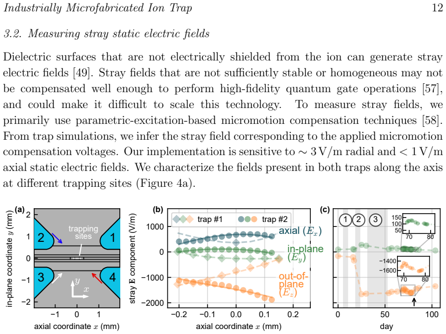
- Stray electric fields can be evaluated and managed across multiple trapping sites.
- Motional heating rates as low as 40 phonons per second occur at 1 MHz and 185 K.
Where Pith is reading between the lines
- The wafer-stacking method could support electrode patterns for multi-zone or segmented traps in a single device.
- Similar industrial processes might extend to other ion species or larger trap arrays without custom machining.
- High-volume production of such traps could lower barriers to building systems with hundreds of ions.
Load-bearing premise
The 2.5 micrometer standard deviation in wafer alignment across the stack does not cause significant degradation of the simulated 1 eV trap depth or introduce problematic stray fields.
What would settle it
A measured trap depth well below 1 eV or unexpectedly high stray fields at the ion position when the fabricated alignment deviation reaches 2.5 micrometers.
Figures



read the original abstract
Scaling trapped-ion quantum computing will require robust trapping of at least hundreds of ions over long periods, while increasing the complexity and functionality of the trap itself. Symmetric 3D structures enable high trap depth, but microfabrication techniques are generally better suited to planar structures that produce less ideal conditions for trapping. We present an ion trap fabricated on stacked 8-inch wafers in a large-scale MEMS microfabrication process that provides reproducible traps at a large volume. Electrodes are patterned on the surfaces of two opposing wafers bonded to a spacer, forming a 3D structure with 2.5 micrometer standard deviation in alignment across the stack. We implement a design achieving a trap depth of 1 eV for a calcium-40 ion held at 200 micrometers from either electrode plane. We characterize traps, achieving measurement agreement with simulations to within +/-5% for mode frequencies spanning 0.6--3.8 MHz, and evaluate stray electric field across multiple trapping sites. We measure motional heating rates over an extensive range of trap frequencies, and temperatures, observing 40 phonons/s at 1 MHz and 185 K. This fabrication method provides a highly scalable approach for producing a new generation of 3D ion traps.
Editorial analysis
A structured set of objections, weighed in public.
Referee Report
Summary. The manuscript reports fabrication of a symmetric 3D ion trap on stacked 8-inch wafers via a large-scale MEMS process, with 2.5 μm alignment std. dev. across the stack. It claims realization of a design with 1 eV trap depth for 40Ca+ at 200 μm from either electrode plane, reports measured trap frequencies agreeing with simulation to within ±5% over 0.6–3.8 MHz, stray-field evaluation at multiple sites, and motional heating rates (e.g., 40 phonons/s at 1 MHz and 185 K) over ranges of frequency and temperature.
Significance. If the 1 eV depth is experimentally realized under the reported alignment tolerance, the work establishes a scalable industrial route to high-depth 3D traps, addressing a key barrier to scaling trapped-ion systems. The extensive heating-rate dataset across trap frequencies and temperatures is a concrete strength that will be useful to the community independent of the depth claim.
major comments (2)
- [Abstract] Abstract: the headline claim of a realized 1 eV trap depth rests on the fabricated geometry matching the simulated ideal, yet only frequency agreement (±5 %) is reported; no direct experimental bound on depth (escape-rate measurement, RF-amplitude scaling to loss, or similar) or sensitivity analysis of depth versus ±2.5 μm electrode shifts is supplied.
- [Fabrication description paragraph] Fabrication description paragraph: the 2.5 μm alignment std. dev. is presented as enabling the 1 eV depth, but without a tolerance study quantifying depth degradation under the observed misalignment distribution, it is impossible to confirm that the simulated value survives fabrication.
minor comments (1)
- [Abstract] The abstract states both 'achieving a trap depth of 1 eV' and 'we implement a design achieving…'; the distinction between simulated design value and measured device performance should be clarified in the main text.
Simulated Author's Rebuttal
We thank the referee for their careful review and for highlighting both the potential impact of the work and the areas needing clarification. We respond to each major comment below.
read point-by-point responses
-
Referee: [Abstract] Abstract: the headline claim of a realized 1 eV trap depth rests on the fabricated geometry matching the simulated ideal, yet only frequency agreement (±5 %) is reported; no direct experimental bound on depth (escape-rate measurement, RF-amplitude scaling to loss, or similar) or sensitivity analysis of depth versus ±2.5 μm electrode shifts is supplied.
Authors: The reported 1 eV depth is obtained from electrostatic simulation of the nominal electrode geometry. The ±5 % agreement between measured and simulated trap frequencies across 0.6–3.8 MHz supplies the primary experimental validation that the fabricated structure reproduces the design. No direct experimental determination of trap depth (e.g., escape-rate or RF-amplitude scaling) was performed. We will add a sensitivity analysis of trap depth versus electrode misalignment of order ±2.5 μm to the revised manuscript. revision: yes
-
Referee: [Fabrication description paragraph] Fabrication description paragraph: the 2.5 μm alignment std. dev. is presented as enabling the 1 eV depth, but without a tolerance study quantifying depth degradation under the observed misalignment distribution, it is impossible to confirm that the simulated value survives fabrication.
Authors: We agree that a quantitative tolerance study is required to substantiate the claim. The revised manuscript will include Monte-Carlo sampling of the measured 2.5 μm alignment distribution to show the resulting distribution of trap depths. revision: yes
- Direct experimental bound on trap depth via escape-rate measurement, RF-amplitude scaling to loss, or equivalent method.
Circularity Check
No significant circularity; central claims rest on experimental measurements validated against independent simulations
full rationale
The paper's core results are direct experimental characterizations (mode frequencies agreeing with simulation to ±5%, stray fields, heating rates) of a fabricated device. The 1 eV trap depth is a design target obtained from electrostatic simulation of the nominal geometry; it is not derived from or fitted to the reported data. No equations reduce reported metrics to parameters defined by the same measurements, no load-bearing self-citations justify uniqueness or ansatzes, and the fabrication tolerances are stated as process outcomes rather than retrofitted to match performance. The derivation chain is therefore self-contained against external experimental benchmarks.
Axiom & Free-Parameter Ledger
axioms (1)
- domain assumption Standard electrostatic simulation of ion traps accurately predicts depth when electrode geometry is known to within fabrication tolerance.
Lean theorems connected to this paper
-
IndisputableMonolith/Foundation/AlexanderDuality.lean; IndisputableMonolith/Cost/FunctionalEquation.leanalexander_duality_circle_linking; washburn_uniqueness_aczel unclear?
unclearRelation between the paper passage and the cited Recognition theorem.
We present an ion trap fabricated on stacked 8-inch wafers … achieving a trap depth of 1 eV … measurement agreement with simulations to within ±5% for mode frequencies spanning 0.6–3.8 MHz
What do these tags mean?
- matches
- The paper's claim is directly supported by a theorem in the formal canon.
- supports
- The theorem supports part of the paper's argument, but the paper may add assumptions or extra steps.
- extends
- The paper goes beyond the formal theorem; the theorem is a base layer rather than the whole result.
- uses
- The paper appears to rely on the theorem as machinery.
- contradicts
- The paper's claim conflicts with a theorem or certificate in the canon.
- unclear
- Pith found a possible connection, but the passage is too broad, indirect, or ambiguous to say the theorem truly supports the claim.
Reference graph
Works this paper leans on
-
[1]
Ion Trap Design and Fabrication 2.1. Trap concept and design Our microfabricated 3D ion trap design, shown in Figure 1a, comprises three wafers. A bottom wafer carries direct current (DC) and radio-frequency (RF) signals on patterned segmented electrodes. Electrodes on the top wafer electrically extend the trap into the third dimension, creating a 3D stru...
-
[2]
Experimental characterization Measurements of traps with ions can validate the simulation, design, and fabrication process. We test our traps by placing them at the lowest-temperature (“base”) cooling stage of a cryogenic apparatus [54] and trapping 40Ca+ ions. Traps are attached to a DC filter board (with first-order, 36 kHz-cutoff-frequency low-pass filters...
work page 2000
-
[3]
Conclusion and Outlook We have demonstrated the operation of a microfabricated MEMS 3D ion trap with a trap depth of 1 eV produced in an industrial facility. Measurements of motional frequencies agreed to within±5% of predicted values over a broad range of DC and RF voltages, validating our simulation model and suggesting that the trap was accurately fabr...
-
[4]
Shor, In Proceedings 35th Annual Symposium on Foundations of Computer Science
P. Shor, In Proceedings 35th Annual Symposium on Foundations of Computer Science . IEEE Comput. Soc. Press, 1994 124–134
work page 1994
-
[5]
L. K. Grover, In Proceedings of the twenty-eighth annual ACM symposium on Theory of computing - STOC '96. ACM Press, 1996 212–219
work page 1996
-
[6]
D. J. Wineland, J. C. Bergquist, J. J. Bollinger, R. E. Drullinger, W. M. Itano, In Frequency Standards and Metrology. World Scientific, 2002 361–368
work page 2002
-
[7]
D. P. DiVincenzo, Science 1995, 270, 5234 255
work page 1995
-
[8]
D. P. DiVincenzo, Fortschritte der Physik 2000
work page 2000
-
[9]
R. Lechner, C. Maier, C. Hempel, P. Jurcevic, B. P. Lanyon, T. Monz, M. Brownnutt, R. Blatt, C. F. Roos, Physical Review A 2016, 93, 5 053401
work page 2016
- [10]
- [11]
-
[12]
M. K. Joshi, A. Fabre, C. Maier, T. Brydges, D. Kiesenhofer, H. Hainzer, R. Blatt, C. F. Roos, New Journal of Physics 2020, 22, 10 103013
work page 2020
-
[13]
R. Srinivas, S. C. Burd, H. M. Knaack, R. T. Sutherland, A. Kwiatkowski, S. Glancy, E. Knill, D. J. Wineland, D. Leibfried, A. C. Wilson, D. T. C. Allcock, D. H. Slichter, Nature 2021, 597, 7875 209
work page 2021
-
[14]
P. Wang, C.-Y. Luan, M. Qiao, M. Um, J. Zhang, Y. Wang, X. Yuan, M. Gu, J. Zhang, K. Kim, Nature Communications 2021, 12, 1
work page 2021
- [15]
-
[16]
J. I. Cirac, P. Zoller, H. J. Kimble, H. Mabuchi, Physical Review Letters 1997, 78, 16 3221
work page 1997
- [17]
- [18]
-
[19]
Y. Wan, D. Kienzler, S. D. Erickson, K. H. Mayer, T. R. Tan, J. J. Wu, H. M. Vasconcelos, S. Glancy, E. Knill, D. J. Wineland, A. C. Wilson, D. Leibfried, Science 2019, 364, 6443 875
work page 2019
-
[20]
J. M. Pino, J. M. Dreiling, C. Figgatt, J. P. Gaebler, S. A. Moses, M. S. Allman, C. H. Baldwin, M. Foss-Feig, D. Hayes, K. Mayer, C. Ryan-Anderson, B. Neyenhuis, Nature 2021, 592, 7853 209
work page 2021
-
[21]
L. E. de Clercq, H.-Y. Lo, M. Marinelli, D. Nadlinger, R. Oswald, V. Negnevitsky, D. Kienzler, B. Keitch, J. P. Home, Physical Review Letters 2016, 116, 8 080502
work page 2016
-
[22]
P. C. Holz, S. Auchter, G. Stocker, M. Valentini, K. Lakhmanskiy, C. R¨ ossler, P. Stampfer, S. Sgouridis, E. Aschauer, Y. Colombe, R. Blatt, Advanced Quantum Technologies 2020, 3, 11 2000031
work page 2020
-
[23]
A. Walther, F. Ziesel, T. Ruster, S. T. Dawkins, K. Ott, M. Hettrich, K. Singer, F. Schmidt-Kaler, U. Poschinger, Physical Review Letters 2012, 109, 8 080501
work page 2012
- [24]
-
[25]
V. Kaushal, B. Lekitsch, A. Stahl, J. Hilder, D. Pijn, C. Schmiegelow, A. Bermudez, M. M¨ uller, F. Schmidt-Kaler, U. Poschinger, AVS Quantum Science 2020, 2, 1 014101
work page 2020
-
[26]
M. D. Hughes, B. Lekitsch, J. A. Broersma, W. K. Hensinger, Contemporary Physics 2011, 52, 6 505
work page 2011
-
[27]
D.-I. D. Cho, S. Hong, M. Lee, T. Kim, Micro and Nano Systems Letters 2015, 3, 1
work page 2015
-
[28]
M. G. Blain, R. Haltli, P. Maunz, C. D. Nordquist, M. Revelle, D. Stick, Quantum Science and Technology 2021, 6, 3 034011
work page 2021
-
[29]
J. Britton, D. Leibfried, J. A. Beall, R. B. Blakestad, J. H. Wesenberg, D. J. Wineland, Applied Physics Letters 2009, 95, 17 173102
work page 2009
-
[30]
J. M. Amini, H. Uys, J. H. Wesenberg, S. Seidelin, J. Britton, J. J. Bollinger, D. Leibfried, Industrially Microfabricated Ion Trap 27 C. Ospelkaus, A. P. VanDevender, D. J. Wineland, New Journal of Physics 2010, 12, 3 033031
work page 2010
-
[31]
S. Seidelin, J. Chiaverini, R. Reichle, J. Bollinger, D. Leibfried, J. Britton, J. Wesenberg, R. Blakestad, R. Epstein, D. Hume, W. Itano, J. Jost, C. Langer, R. Ozeri, N. Shiga, D. Wineland, Physical Review Letters 2006, 96, 25
work page 2006
-
[32]
J. Chiaverini, R. B. Blakestad, J. Britton, J. D. Jost, C. Langer, D. Leibfried, R. Ozeri, D. J. Wineland, Quantum Inf. Comput. 2005, 5, 6 419
work page 2005
-
[33]
S. C. Doret, J. M. Amini, K. Wright, C. Volin, T. Killian, A. Ozakin, D. Denison, H. Hayden, C.-S. Pai, R. E. Slusher, A. W. Harter, New Journal of Physics 2012, 14, 7 073012
work page 2012
- [34]
-
[35]
W. K. Hensinger, S. Olmschenk, D. Stick, D. Hucul, M. Yeo, M. Acton, L. Deslauriers, C. Monroe, J. Rabchuk, Applied Physics Letters 2006, 88, 3 034101
work page 2006
-
[36]
R. B. Blakestad, C. Ospelkaus, A. P. VanDevender, J. M. Amini, J. Britton, D. Leibfried, D. J. Wineland, Physical Review Letters 2009, 102, 15
work page 2009
-
[37]
C. Decaroli, R. Matt, R. Oswald, C. Axline, M. Ernzer, J. Flannery, S. Ragg, J. P. Home,Quantum Science and Technology 2021, 6, 4 044001
work page 2021
-
[38]
C. D. Bruzewicz, J. Chiaverini, R. McConnell, J. M. Sage, Applied Physics Reviews 2019, 6, 2 021314
work page 2019
-
[39]
G. Wilpers, P. See, P. Gill, A. G. Sinclair, Nature Nanotechnology 2012, 7, 9 572
work page 2012
-
[40]
K. R. Brown, J. Chiaverini, J. M. Sage, H. H¨ affner, Nature Reviews Materials 2021
work page 2021
-
[41]
J. H. Wesenberg, Physical Review A 2008, 78, 6 063410
work page 2008
-
[42]
M. F. Brandl, M. W. van Mourik, L. Postler, A. Nolf, K. Lakhmanskiy, R. R. Paiva, S. M¨ oller, N. Daniilidis, H. H¨ affner, V. Kaushal, T. Ruster, C. Warschburger, H. Kaufmann, U. G. Poschinger, F. Schmidt-Kaler, P. Schindler, T. Monz, R. Blatt, Review of Scientific Instruments 2016, 87, 11 113103
work page 2016
- [43]
- [44]
-
[45]
D. Douglas, A. Berdnikov, N. Konenkov, International Journal of Mass Spectrometry 2015, 377 345
work page 2015
-
[46]
K. K. Mehta, C. Zhang, M. Malinowski, T.-L. Nguyen, M. Stadler, J. P. Home, Nature 2020, 586, 7830 533
work page 2020
-
[47]
D. I. Schuster, L. S. Bishop, I. L. Chuang, D. DeMille, R. J. Schoelkopf, Physical Review A 2011, 83, 1 012311
work page 2011
-
[48]
R. B. Blakestad, Ph.D. thesis, California Institute of Technology, 2010
work page 2010
-
[49]
D. T. C. Allcock, J. A. Sherman, D. N. Stacey, A. H. Burrell, M. J. Curtis, G. Imreh, N. M. Linke, D. J. Szwer, S. C. Webster, A. M. Steane, D. M. Lucas, New Journal of Physics 2010, 12, 5 053026
work page 2010
- [50]
-
[51]
K. K. Mehta, A. M. Eltony, C. D. Bruzewicz, I. L. Chuang, R. J. Ram, J. M. Sage, J. Chiaverini, Applied Physics Letters 2014, 105, 4 044103
work page 2014
- [52]
- [53]
-
[54]
E. Peeters, S. Vergote, B. Puers, W. Sansen, Journal of Micromechanics and Microengineering 1992, 2, 3 167
work page 1992
- [55]
-
[56]
J. He, F. Yang, W. Wang, L. Zhang, X. Huang, D. Zhang, Journal of Micromechanics and Industrially Microfabricated Ion Trap 28 Microengineering 2015, 25, 6 065002
work page 2015
- [57]
-
[58]
H. C. J. Gan, G. Maslennikov, K.-W. Tseng, T. R. Tan, R. Kaewuam, K. J. Arnold, D. Matsukevich, M. D. Barrett, Physical Review A 2018, 98, 3 032514
work page 2018
- [59]
-
[60]
C. J. Ballance, Ph.D. thesis, Oxford University, Cham, 2017, URL http://link.springer. com/10.1007/978-3-319-68216-7
-
[61]
D. J. Wineland, C. R. Monroe, W. M. Itano, D. Leibfried, B. E. King, D. M. Meekhof, Journal of Research of the National Institute of Standards and Technology 1998, 103 259
work page 1998
-
[62]
J. T. Merrill, C. Volin, D. Landgren, J. M. Amini, K. Wright, S. C. Doret, C.-S. Pai, H. Hayden, T. Killian, D. Faircloth, K. R. Brown, A. W. Harter, R. E. Slusher, New Journal of Physics 2011, 13, 10 103005
work page 2011
-
[63]
S. Narayanan, N. Daniilidis, S. A. M¨ oller, R. Clark, F. Ziesel, K. Singer, F. Schmidt-Kaler, H. H¨ affner,Journal of Applied Physics 2011, 110, 11 114909
work page 2011
-
[64]
C. R. Clark, C. wen Chou, A. Ellis, J. Hunker, S. A. Kemme, P. Maunz, B. Tabakov, C. Tigges, D. L. Stick, Physical Review Applied 2014, 1, 2 024004
work page 2014
-
[65]
G. Shu, G. Vittorini, A. Buikema, C. S. Nichols, C. Volin, D. Stick, K. R. Brown, Physical Review A 2014, 89, 6 062308
work page 2014
-
[66]
M. Harlander, M. Brownnutt, W. H¨ ansel, R. Blatt, New Journal of Physics 2010, 12, 9 093035
work page 2010
-
[67]
S. X. Wang, G. H. Low, N. S. Lachenmyer, Y. Ge, P. F. Herskind, I. L. Chuang, Journal of Applied Physics 2011, 110, 10 104901
work page 2011
-
[68]
F. R. Ong, K. Sch¨ uppert, P. Jobez, M. Teller, B. Ames, D. A. Fioretto, K. Friebe, M. Lee, Y. Colombe, R. Blatt, T. E. Northup, New Journal of Physics 2020, 22, 6 063018
work page 2020
-
[69]
D. T. C. Allcock, T. P. Harty, H. A. Janacek, N. M. Linke, C. J. Ballance, A. M. Steane, D. M. Lucas, R. L. Jarecki, S. D. Habermehl, M. G. Blain, D. Stick, D. L. Moehring, Applied Physics B 2011, 107, 4 913
work page 2011
-
[70]
J. M. McGuirk, D. M. Harber, J. M. Obrecht, E. A. Cornell, Physical Review A 2004, 69, 6 062905
work page 2004
-
[71]
J. M. Obrecht, R. J. Wild, E. A. Cornell, Physical Review A 2007, 75, 6 062903
work page 2007
- [72]
- [73]
- [74]
-
[75]
Q. A. Turchette, Kielpinski, B. E. King, D. Leibfried, D. M. Meekhof, C. J. Myatt, M. A. Rowe, C. A. Sackett, C. S. Wood, W. M. Itano, C. Monroe, D. J. Wineland, Physical Review A 2000, 61, 6 063418
work page 2000
-
[76]
M. Brownnutt, M. Kumph, P. Rabl, R. Blatt, Reviews of Modern Physics 2015, 87, 4 1419
work page 2015
-
[77]
D. Leibfried, R. Blatt, C. Monroe, D. Wineland, Reviews of Modern Physics 2003, 75, 1 281
work page 2003
- [78]
-
[79]
W. J. Kim, A. O. Sushkov, D. A. R. Dalvit, S. K. Lamoreaux, Physical Review A 2010, 81, 2 022505
work page 2010
-
[80]
S. X. Wang, Y. Ge, J. Labaziewicz, E. Dauler, K. Berggren, I. L. Chuang, Applied Physics Letters 2010, 97, 24 244102
work page 2010
discussion (0)
Sign in with ORCID, Apple, or X to comment. Anyone can read and Pith papers without signing in.