Recognition: unknown
ALD W-Doped SnO₂ TFTs for Indium-Free BEOL Electronics
Pith reviewed 2026-05-10 15:41 UTC · model grok-4.3
The pith
Low-temperature ALD of 10% tungsten-doped tin oxide produces indium-free TFTs with 10^9 on/off ratio and strong bias stability after brief oxygen annealing.
A machine-rendered reading of the paper's core claim, the machinery that carries it, and where it could break.
Core claim
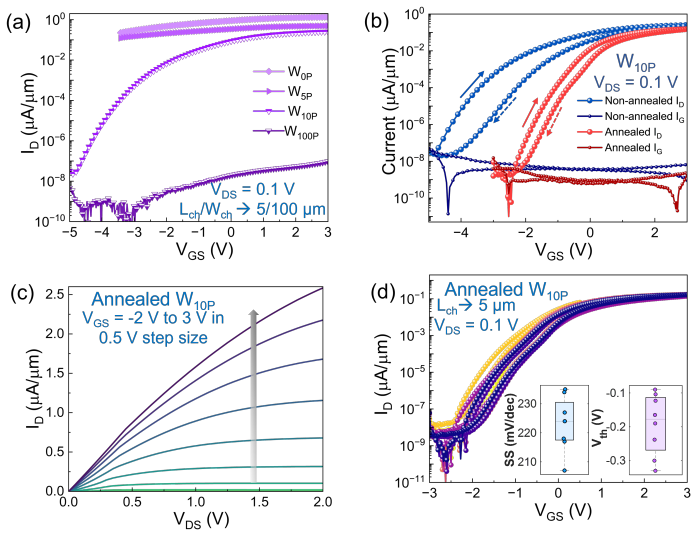
TFTs with 10% W doping in SnOx channels deposited by ALD at 150°C, after 300°C O2 annealing for 5 minutes, achieve a subthreshold swing reduced by nearly 2 times, Ion/Ioff ratio of 10^9, hysteresis decreased by 3 times, and bias stress threshold shift of only 93 mV at 4 MV/cm. Kinetic Monte Carlo simulations attribute the remaining instability to charge trapping. This establishes low-temperature ALD W-doped SnO2 as a viable indium-free material for BEOL compatible transistors and monolithic 3D integration.
What carries the argument
The 10% tungsten-doped tin oxide channel deposited by atomic layer deposition at 150°C and enhanced by short oxygen annealing, which improves carrier control and reduces defects leading to better device metrics.
Load-bearing premise
The observed benefits of W doping and O2 annealing will persist when these transistors are built directly atop finished CMOS circuits without introducing damage or additional reliability problems at production scales.
What would settle it
Measuring significant degradation in performance or damage to underlying CMOS layers when fabricating the TFTs on actual integrated circuits would disprove the BEOL compatibility claim.
Figures


read the original abstract
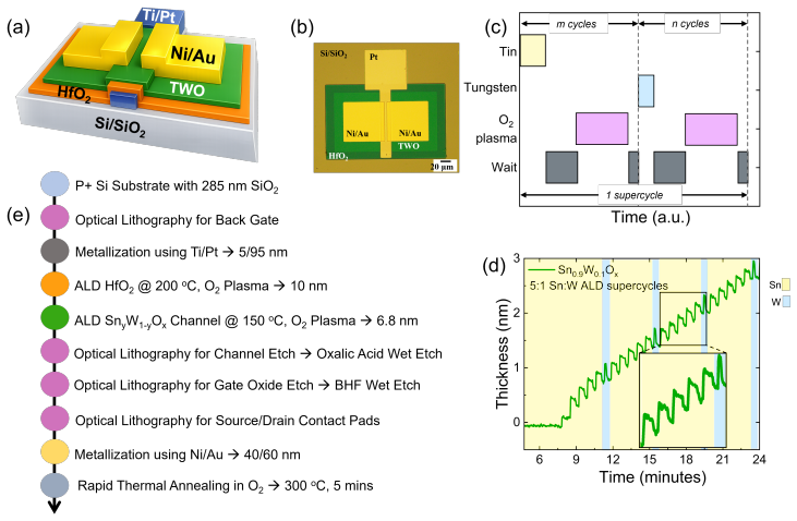
This work reports back-end-of-line (BEOL) compatible, thin-film transistors (TFTs) with sub-10 nm tungsten-doped tin oxide (TWO) channels deposited by atomic layer deposition (ALD) at 150 $^\circ$C. TFTs with undoped SnO$_{\mathrm{x}}$, undoped WO$_{\mathrm{x}}$, and W-doped SnO$_{\mathrm{x}}$ channels with W concentrations of 5% and 10% were investigated. TFT with 10% W doping exhibited the best electrostatic control and overall device performance. Post-fabrication O$_{\mathrm{2}}$ annealing at 300 $^\circ$C for 5 minutes significantly enhanced device characteristics, reducing the subthreshold swing (SS) by nearly 2$\times$, increasing the I$_{\mathrm{on}}$/I$_{\mathrm{off}}$ ratio from $10^7$ to $10^9$, decreasing hysteresis by nearly 3$\times$ and positive bias stress-induced threshold shift by over 2$\times$ to a low value of 93 mV at a stress field of 4 MV/cm. Kinetic Monte Carlo simulations using Ginestra$^{\mathrm{TM}}$ support the experimental observations and attribute the bias instability to charge trapping in the gate dielectric and at the interface. This work demonstrates low-temperature ALD-grown TWO TFTs as a promising indium-free platform for BEOL and monolithic 3D integration.
Editorial analysis
A structured set of objections, weighed in public.
Referee Report
Summary. The manuscript reports fabrication of back-end-of-line (BEOL) compatible thin-film transistors (TFTs) with sub-10 nm tungsten-doped tin oxide (TWO) channels grown by atomic layer deposition (ALD) at 150°C. Devices with undoped SnOx, undoped WOx, and W-doped channels at 5% and 10% W were compared; the 10% W variant showed best electrostatic control. A post-fabrication 300°C O2 anneal for 5 min improved subthreshold swing by ~2×, raised Ion/Ioff from 10^7 to 10^9, reduced hysteresis by ~3×, and lowered positive-bias-stress threshold shift to 93 mV at 4 MV/cm. Ginestra kinetic Monte Carlo simulations attribute the remaining instability to dielectric and interface charge trapping. The work positions low-temperature ALD TWO TFTs as a promising indium-free platform for BEOL and monolithic 3D integration.
Significance. If the thermal-budget compatibility holds, the concrete metrics (high Ion/Ioff, low SS, reduced hysteresis and stress shift) plus simulation backing would constitute a useful experimental demonstration of an indium-free oxide TFT route for BEOL electronics. The annealing-induced improvements and the trapping-based explanation of bias instability are clear strengths of the reported data set.
major comments (1)
- [Conclusion / BEOL compatibility discussion] The central claim that these TFTs constitute a 'promising indium-free platform for BEOL' is load-bearing yet rests on an untested assumption: that the 300°C/5 min O2 anneal (and the full TWO flow) can be performed on actual CMOS wafers without damaging interconnects or pre-existing devices. No data on via resistance, metal-line integrity, or shifts in underlying transistors after the anneal are provided; all metrics come from test substrates only.
minor comments (2)
- [Experimental methods] State the exact method (XPS, EDX, etc.) and any uncertainty used to determine the 5% and 10% W concentrations in the channel.
- [Results and discussion] Include error bars or standard deviations on the reported SS, Ion/Ioff, hysteresis, and ΔVth values, and clarify the number of devices measured per condition.
Simulated Author's Rebuttal
We thank the referee for the detailed and constructive report. The single major comment is addressed point-by-point below. We have revised the manuscript to acknowledge the limitation while preserving the technical contribution of the low-temperature ALD TWO process.
read point-by-point responses
-
Referee: The central claim that these TFTs constitute a 'promising indium-free platform for BEOL' is load-bearing yet rests on an untested assumption: that the 300°C/5 min O2 anneal (and the full TWO flow) can be performed on actual CMOS wafers without damaging interconnects or pre-existing devices. No data on via resistance, metal-line integrity, or shifts in underlying transistors after the anneal are provided; all metrics come from test substrates only.
Authors: We agree that all electrical data were obtained on Si/SiO2 test substrates and that no direct measurements of via resistance, Cu-line integrity, or shifts in underlying CMOS transistors after the 300 °C/5 min O2 anneal are presented. The 150 °C ALD deposition and 300 °C anneal were deliberately chosen to lie well below the typical 400 °C BEOL thermal ceiling, and the Ginestra simulations confirm that the observed bias instability originates from dielectric/interface trapping rather than channel crystallization. In the revised manuscript we have (i) added an explicit limitations paragraph in the Discussion section stating that full BEOL integration studies remain future work, (ii) changed the abstract and conclusion phrasing from “promising indium-free platform” to “potential indium-free route whose thermal budget is compatible with BEOL processing,” and (iii) included a brief comparison to literature reports that similarly claim BEOL compatibility on the basis of process temperature alone. These changes make the scope of the present study clear without altering the reported device metrics or simulation results. revision: partial
Circularity Check
No circularity: experimental metrics and supporting simulation are independent of any fitted derivation
full rationale
The manuscript is a fabrication-and-measurement study of ALD TWO TFTs. All reported device metrics (SS, Ion/Ioff, hysteresis, PBS shift) are directly measured on fabricated devices before and after O2 anneal; the Ginestra KMC runs are used only to reproduce the observed threshold shifts under a charge-trapping model. No equations, ansatzes, or parameter fits are presented as predictions that reduce to the inputs by construction. No self-citations supply load-bearing uniqueness theorems or ansatzes. The central claim therefore rests on empirical data rather than any self-referential derivation chain.
Axiom & Free-Parameter Ledger
axioms (1)
- domain assumption Standard assumptions of ALD growth uniformity and TFT electrostatic models hold for sub-10 nm channels.
Reference graph
Works this paper leans on
-
[1]
merlin.mbs aapmrev4-1.bst 2010-07-25 4.21a (PWD, AO, DPC) hacked
FUNCTION id.bst "merlin.mbs aapmrev4-1.bst 2010-07-25 4.21a (PWD, AO, DPC) hacked" ENTRY address archive archivePrefix author bookaddress booktitle chapter collaboration doi edition editor eid eprint howpublished institution isbn issn journal key language month note number organization pages primaryClass publisher school SLACcitation series title translat...
2010
-
[2]
merlin.mbs aipauth4-1.bst 2010-07-25 4.21a (PWD, AO, DPC) hacked
FUNCTION id.bst "merlin.mbs aipauth4-1.bst 2010-07-25 4.21a (PWD, AO, DPC) hacked" ENTRY address archive archivePrefix author bookaddress booktitle chapter collaboration doi edition editor eid eprint howpublished institution isbn issn journal key language month note number organization pages primaryClass publisher school SLACcitation series title translat...
2010
-
[3]
merlin.mbs aipnum4-1.bst 2010-07-25 4.21a (PWD, AO, DPC) hacked
FUNCTION id.bst "merlin.mbs aipnum4-1.bst 2010-07-25 4.21a (PWD, AO, DPC) hacked" ENTRY address archive archivePrefix author bookaddress booktitle chapter collaboration doi edition editor eid eprint howpublished institution isbn issn journal key language month note number organization pages primaryClass publisher school SLACcitation series title translati...
2010
-
[4]
Nomura , author H
author author K. Nomura , author H. Ohta , author A. Takagi , author T. Kamiya , author M. Hirano , \ and\ author H. Hosono ,\ title title Room-temperature fabrication of transparent flexible thin-film transistors using amorphous oxide semiconductors , \ @noop journal journal nature \ volume 432 ,\ pages 488--492 ( year 2004 ) NoStop
2004
-
[5]
Hosono ,\ title title How we made the IGZO transistor , \ @noop journal journal Nature Electronics \ volume 1 ,\ pages 428 ( year 2018 ) NoStop
author author H. Hosono ,\ title title How we made the IGZO transistor , \ @noop journal journal Nature Electronics \ volume 1 ,\ pages 428 ( year 2018 ) NoStop
2018
-
[6]
Kamiya \ and\ author H
author author T. Kamiya \ and\ author H. Hosono ,\ title title Material characteristics and applications of transparent amorphous oxide semiconductors , \ @noop journal journal NPG Asia Materials \ volume 2 ,\ pages 15--22 ( year 2010 ) NoStop
2010
-
[7]
author author H. Hosono ,\ title title Ionic amorphous oxide semiconductors: Material design, carrier transport, and device application , \ @noop journal journal Journal of non-crystalline solids \ volume 352 ,\ pages 851--858 ( year 2006 ) NoStop
2006
-
[8]
author author Y. G. Y. H. \ Yongli He , Xiangyu Wang \ and\ author Q. Wan ,\ title title Oxide-based thin film transistors for flexible electronics , \ @noop journal journal Journal of Semiconductors \ volume 39 ,\ pages 011005 ( year 2018 ) NoStop
2018
-
[9]
author author J. S. \ Nathan , A. ,\ title title Oxide electronics: Translating materials science from lab-to-fab , \ @noop journal journal MRS Bulletin \ volume 46 ,\ pages 1028--1036 ( year 2021 ) NoStop
2021
-
[10]
author author M. Mirshojaeian Hosseini ,\ title title A review of the progress of thin-film transistors and their technologies for flexible electronics , \ @noop journal journal Micromachines \ volume 12 ,\ pages 655 ( year 2021 ) NoStop
2021
-
[11]
author author J. J. \ Avis C ,\ title title In _2 O _3 : An oxide semiconductor for thin-film transistors , \ @noop journal journal Molecules \ volume 30 ,\ pages 4762 ( year 2025 ) NoStop
2025
-
[12]
Si , author Y
author author M. Si , author Y. Hu , author Z. Lin , author X. Sun , author A. Charnas , author D. Zheng , author X. Lyu , author H. Wang , author K. Cho , \ and\ author P. D. \ Ye ,\ title title Why In _2 O _3 can make 0.7 nm atomic layer thin transistors , \ @noop journal journal Nano Letters \ volume 21 ,\ pages 500--506 ( year 2021 ) NoStop
2021
-
[13]
Park , author S
author author H. Park , author S. Gopal Kirtania , author E. Sarkar , author D. Chakraborty , author C. Zhang , author H. Jae Lee , author J. Shin , author S. Yu , author A. Khan , author H. Kim , author C. Im , author M. J. \ Hong , author D. Ha , \ and\ author S. Datta ,\ title title Extreme eot scaling in tungsten-doped In _2 O _3 mosfets for enhanced ...
2025
-
[14]
Britannica ,\ https://www.britannica.com/science/indium title Indium , \ ( year 2024 ) NoStop
author author E. Britannica ,\ https://www.britannica.com/science/indium title Indium , \ ( year 2024 ) NoStop
2024
-
[15]
author author U. G. \ Survey ,\ https://pubs.usgs.gov/periodicals/mcs2025/mcs2025.pdf title Mineral commodity summaries 2025 , \ type Tech. Rep. \ ( year 2025 ) NoStop
2025
-
[16]
author author G. K. \ Dalapati , author H. Sharma , author A. Guchhait , author N. Chakrabarty , author P. Bamola , author Q. Liu , author G. Saianand , author A. M. S. \ Krishna , author S. Mukhopadhyay , author A. Dey , author T. K. S. \ Wong , author S. Zhuk , author S. Ghosh , author S. Chakrabortty , author C. Mahata , author S. Biring , author A. Ku...
2021
-
[17]
He , author X
author author Z. He , author X. Zhang , author X. Wei , author D. Luo , author H. Ning , author Q. Ye , author R. Wu , author Y. Guo , author R. Yao , \ and\ author J. Peng ,\ title title Solution-processed Silicon Doped Tin Oxide Thin Films and Thin-Film Transistors Based on Tetraethyl Orthosilicate , \ @noop \ volume 12 ,\ pages 590 ( year 2022 ) NoStop
2022
-
[18]
author author W. S. \ Kim , author K. H. \ Lee , et al. ,\ title title Improvement in the bias stability of tin oxide thin-film transistors by hafnium doping , \ @noop journal journal Thin Solid Films \ volume 520 ,\ pages 2220--2223 ( year 2012 ) NoStop
2012
-
[19]
author author C. A. F. L. C. e. a. \ Wei Shih , C. ,\ title title Remarkably high mobility ultra-thin-film metal-oxide transistor with strongly overlapped orbitals , \ @noop journal journal Scientific Reports \ volume 6 ,\ pages 19023 ( year 2016 ) NoStop
2016
-
[20]
author author B. K. \ Lee , author E. Jung , author S. H. \ Kim , author D. C. \ Moon , author S. S. \ Lee , author B. K. \ Park , author J. H. \ Hwang , author T.-M. \ Chung , author C. G. \ Kim , \ and\ author K.-S. \ An ,\ title title Physical/chemical properties of tin oxide thin film transistors prepared using plasma-enhanced atomic layer deposition ...
2012
-
[21]
\ Han , author J.-H
author author D.-S. \ Han , author J.-H. \ Park , author Y.-J. \ Kang , \ and\ author J.-W. \ Park ,\ title title Effects of zirconium doping on the characteristics of tin oxide thin film transistors , \ @noop journal journal Microelectronics Reliability \ volume 53 ,\ pages 1875--1878 ( year 2013 ) NoStop
2013
-
[22]
author author H. Q. \ Chiang , author J. F. \ Wager , author R. L. \ Hoffman , author J. Jeong , \ and\ author D. A. \ Keszler ,\ title title High mobility transparent thin-film transistors with amorphous zinc tin oxide channel layer , \ @noop journal journal Applied Physics Letters \ volume 86 ,\ pages 013503 ( year 2004 ) NoStop
2004
-
[23]
author author C. W. N. H. Z. X. Y. W. X. M.-W. X. Y. R. P. J. \ Liu X , Wu W ,\ title title Enhancement of electrical characteristics and stability of amorphous Si-Sn-O thin film transistors with SiO _x passivation layer , \ @noop journal journal Materials \ volume 11 ,\ pages 1440 ( year 2018 ) NoStop
2018
-
[24]
author author J. C. Z. F. H. N. S. H. R. T.-Y. Z. Z. Z. R. Y. \ Xianzhe Liu , Wei Cai ,\ title title A novel nondestructive testing method for amorphous Si–Sn–O films , \ @noop journal journal J. Phys. D: Appl. Phys. \ volume 49 ,\ pages 505102 ( year 2016 ) NoStop
2016
-
[25]
author author D. L. Y. H. M. Q. S. P. R. F. \ Jianwen Yang , Jinhua Ren \ and\ author Q. Zhang ,\ title title Amorphous nickel incorporated tin oxide thin film transistors , \ @noop journal journal J. Phys. D: Appl. Phys. \ volume 50 ,\ pages 355103 ( year 2017 ) NoStop
2017
-
[26]
author author Y. K. D. N. M. F. . M. K. \ Tokiyoshi Matsuda , Kenta Umeda ,\ title title Rare-metal-free high-performance Ga-Sn-O thin film transistor , \ @noop journal journal Scientific Reports \ volume 7 ,\ pages 44326 ( year 2017 ) NoStop
2017
-
[27]
author author S. H. C. L. J.-H. B. I.-M. K. \ Won-Yong Lee , Hyunjae Lee \ and\ author J. Jang ,\ title title Improved negative bias stability of sol–gel processed ti-doped SnO _2 thin-film transistors , \ @noop journal journal Semiconductor Science and Technology. \ volume 35 ,\ pages 115023 ( year 2020 ) NoStop
2020
-
[28]
author author H. S. L. C. B. J.-H. K. I.-M. K. K. J. J. \ Lee W-Y , Lee H ,\ title title Effect of mg doping on the electrical performance of a sol-gel-processed SnO _2 thin-film transistors , \ @noop journal journal Electronics \ volume 9 ,\ pages 523 ( year 2020 ) NoStop
2020
-
[29]
author author Z. Y. C. C. \ Jianwen Yang , Ting Meng \ and\ author Q. Zhang ,\ title title Investigation of Tungsten Doped SnO _2 Thin Film Transistors , \ @noop journal journal J. Phys. D: Appl. Phys \ volume 48 ,\ pages 435108 ( year 2015 ) NoStop
2015
-
[30]
Roose \ and\ author R
author author B. Roose \ and\ author R. H. \ Friend ,\ title title Extrinsic Electron Concentration in SnO _2 Electron Extracting Contact in Lead Halide Perovskite Solar Cells , \ @noop journal journal Advanced Materials Interfaces. \ volume 6 ,\ pages 1801788 ( year 2019 ) NoStop
2019
-
[31]
author author R. R. B. \ P. Senthilkumar , S. Raja \ and\ author G. Vasuki ,\ title title Enhanced Electrical and Optoelectronic Properties of W Doped SnO _2 Thin Films , \ @noop journal journal Optical Materials \ volume 126 ,\ pages 112234 ( year 2022 ) NoStop
2022
-
[32]
Liu , author H
author author X. Liu , author H. Ning , author J. Chen , author W. Cai , author S. Hu , author R. Tao , author Y. Zeng , author Z. Zheng , author R. Yao , author M. Xu , author L. Wang , author L. Lan , \ and\ author J. Peng ,\ title title High-Performance Back-Channel-Etched Thin-Film Transistors with Amorphous Si-Incorporated SnO _2 Active Layer , \ @no...
2016
-
[33]
\ Jo , author S.-W
author author K.-W. \ Jo , author S.-W. \ Moon , \ and\ author W.-J. \ Cho ,\ title title Fabrication of High-Performance Ultra-Thin-Body SnO _2 Thin-Film Transistors Using Microwave-Irradiation Post-Deposition Annealing , \ @noop journal journal Applied Physics Letters \ volume 106 ,\ pages 043501 ( year 2015 ) NoStop
2015
-
[34]
author author L. Z. Q. W. C. L. \ Yu Yao , Dandan Sang ,\ title title A review on the properties and applications of WO _3 nanostructure-based optical and electronic devices , \ @noop journal journal Nanomaterials (Basel) \ volume 11 ,\ pages 2136 ( year 2021 ) NoStop
2021
-
[35]
Zhou , author Z
author author S. Zhou , author Z. Yang , author X. Feng , author J. Zuo , author N. Wang , author K. Thummavichai , \ and\ author Y. Zhu ,\ title title The frontier of tungsten oxide nanostructures in electronic applications , \ @noop journal journal iScience \ volume 27 ,\ pages 109535 ( year 2024 ) NoStop
2024
-
[36]
Mandal , author A
author author R. Mandal , author A. Mandal , author A. Dutta , author R. Sivakumar , author S. K. \ Srivastava , \ and\ author T. Som ,\ title title Controllable physicochemical properties of WO _x thin films grown under glancing angle , \ @noop journal journal Beilstein Journal of Nanotechnology \ volume 15 ,\ pages 350--359 ( year 2024 ) NoStop
2024
-
[37]
author author Y. H. H. \ Seok-Jun Seo , Chaun Gi Choi \ and\ author B.-S. \ Bae ,\ title title High performance solution-processed amorphous zinc tin oxide thin film transistor , \ @noop journal journal J. Phys. D: Appl. Phys. \ volume 42 ,\ pages 035106 ( year 2008 ) NoStop
2008
-
[38]
author author Applied Materials Ginestra ^ TM ,\ @noop note https://www.appliedmaterials.com/us/en/semiconductor/solutions-and-software/software-solutions/ginestra-simulation-platform.html NoStop
-
[39]
author author K. T. \ Vogt , author C. E. \ Malmberg , author J. C. \ Buchanan , author G. W. \ Mattson , author G. M. \ Brandt , author D. B. \ Fast , author P. H.-Y. \ Cheong , author J. F. \ Wager , \ and\ author M. W. \ Graham ,\ title title Ultrabroadband density of states of amorphous In-Ga-Zn-O , \ @noop journal journal Phys. Rev. Res. \ volume 2 ,...
2020
-
[40]
cold-passivation
author author E. e. a. \ Rucavado ,\ title title New route for "cold-passivation" of defects in tin-based oxides , \ @noop journal journal The journal of physical chemistry \ volume 122 ,\ pages 17612--17620 ( year 2018 ) NoStop
2018
-
[41]
Ponte , author E
author author R. Ponte , author E. Rauwel , \ and\ author P. Rauwel ,\ title title Tailoring SnO _2 defect states and structure: Reviewing bottom-up approaches to control size, morphology, electronic and electrochemical properties for application in batteries , \ @noop journal journal Materials \ volume 16 ,\ pages 4339 ( year 2023 ) NoStop
2023
-
[42]
Wang , author J
author author Z. Wang , author J. Zheng , author M. Li , author Q. Wu , author B. Huang , author C. Chen , author J. Wu , \ and\ author C. Liu ,\ title title Solution-based SnGaO thin-film transistors for zn- and in-free oxide electronic devices , \ @noop journal journal Applied Physics Letters \ volume 113 ,\ pages 122101 ( year 2018 ) NoStop
2018
-
[43]
author author S. A. D. C. \ Zhang W , Fan Z ,\ title title Atmosphere effect in post-annealing treatments for amorphous InGaZnO thin-film transistors with SiO _x passivation layers , \ @noop journal journal Micromachines \ volume 12 ,\ pages 1551 ( year 2021 ) NoStop
2021
-
[44]
Qu , author C.-H
author author M. Qu , author C.-H. \ Chang , author T. Meng , author Q. Zhang , author P.-T. \ Liu , \ and\ author H.-P. D. \ Shieh ,\ title title Stability study of indium tungsten oxide thin-film transistors annealed under various ambient conditions , \ @noop journal journal physica status solidi (a) \ volume 214 ,\ pages 1600465 ( year 2016 ) NoStop
2016
-
[45]
\ Jeong , author H
author author H.-S. \ Jeong , author H. S. \ Cha , author S. H. \ Hwang , \ and\ author H.-I. \ Kwon ,\ title title Effects of annealing atmosphere on electrical performance and stability of high-mobility Indium-Gallium-Tin Oxide Thin-Film Transistors , \ @noop journal journal Electronics \ volume 9 ,\ pages 1875 ( year 2020 ) NoStop
2020
-
[46]
\ Kim , author Y.-K
author author W.-S. \ Kim , author Y.-K. \ Moon , author K.-T. \ Kim , author S.-Y. \ Shin , \ and\ author J.-W. \ Park ,\ title title Improvement in the bias stability of tin oxide thin-film transistors by hafnium doping , \ @noop journal journal Thin Solid Films \ volume 520 ,\ pages 2220--2223 ( year 2012 ) NoStop
2012
-
[47]
Yoo , author J
author author C. Yoo , author J. Hartanto , author B. Saini , author W. Tsai , author V. Thampy , author S. S. \ Niavol , author A. C. \ Meng , \ and\ author P. C. \ McIntyre ,\ title title Atomic layer deposition of WO _3 -doped In _2 O _3 for reliable and scalable BEOL -compatible transistors , \ @noop journal journal Nano Letters \ volume 24 ,\ pages 5...
2024
-
[48]
Zhang , author Z
author author Z. Zhang , author Z. Lin , author C. Niu , author M. Si , author M. A. \ Alam , \ and\ author P. D. \ Ye ,\ title title Ultrahigh bias stability of ALD In _2 O _3 fets enabled by high temperature O _2 annealing , \ in\ @noop booktitle 2023 IEEE Symposium on VLSI Technology and Circuits (VLSI Technology and Circuits) \ ( year 2023 )\ pp.\ pag...
2023
-
[49]
Zheng , author A
author author D. Zheng , author A. Charnas , author J. Anderson , author H. Dou , author Z. Hu , author Z. Lin , author Z. Zhang , author J. Zhang , author P.-Y. \ Liao , author M. Si , author H. Wang , author D. Weinstein , \ and\ author P. D. \ Ye ,\ title title First demonstration of BEOL -compatible ultrathin atomic-layer-deposited InZnO transistors w...
2022
-
[50]
author author S. H. Y. H. C.-C. K. P.-S. H. L. M. H. C. B. J. K. \ Jae Seok Hur , Min Jae Kim \ and\ author J. K. \ Jeong ,\ title title High-performance thin-film transistor with atomic layer deposition ( ALD )-derived indium–gallium oxide channel for back-end-of-line compatible transistor applications: Cation combinatorial approach , \ @noop journal jou...
2022
-
[51]
Park , author J
author author K. Park , author J. H. \ Kim , author T. Sung , author H.-W. \ Park , author J.-H. \ Baeck , author J. Bae , author K.-S. \ Park , author S. Yoon , author I. Kang , author K.-B. \ Chung , author H.-S. \ Kim , \ and\ author J.-Y. \ Kwon ,\ title title Highly reliable amorphous In-Ga-Zn-O thin-film transistors through the addition of nitrogen ...
2019
-
[52]
Zhou , author X
author author X. Zhou , author X. Zhang , author Y. Shao , author L. Zhang , author H. He , author D. Han , author Y. Wang , \ and\ author S. Zhang ,\ title title P-6.1: Asymmetric effects of gate-bias stress voltage on the stability under positive and negative gate-bias stress of a-IGZO tfts , \ @noop journal journal SID Symposium Digest of Technical Pap...
2018
-
[53]
Hu , author K
author author Y. Hu , author K. A. \ Aabrar , author A. Palmieri , author M. Bergschneider , author M. Pešić , author C. D. \ Young , author S. Datta , \ and\ author K. Cho ,\ title title On the dopant, defect states, and mobility in w doped amorphous In _2 O _3 for BEOL transistors , \ in\ @noop booktitle "2023 7th IEEE Electron Devices Technology & Manu...
2023
-
[54]
Hoang , author A
author author L. Hoang , author A. Daus , author S. Wahid , author J. Kwon , author J.-S. \ Ko , author S. Qin , author M. Islam , author K. C. \ Saraswat , author H.-S. P. \ Wong , \ and\ author E. Pop ,\ title title Bias stress stability of ITO transistors and its dependence on dielectric properties , \ in\ @noop booktitle 2022 Device Research Conferenc...
2022
-
[55]
Zhang , author S
author author Q. Zhang , author S. Shao , author Z. Chen , author V. Pecunia , author K. Xia , author J. Zhao , \ and\ author Z. Cui ,\ title title High-resolution inkjet-printed oxide thin-film transistors with a self-aligned fine channel bank structure , \ @noop journal journal ACS Applied Materials & Interfaces \ volume 10 ,\ pages 15847--15854 ( year ...
2018
-
[56]
Zheng , author A
author author D. Zheng , author A. Charnas , author J. Anderson , author H. Dou , author Z. Hu , author Z. Lin , author Z. Zhang , author J. Zhang , author P.-Y. \ Liao , author M. Si , author H. Wang , author D. Weinstein , \ and\ author P. D. \ Ye ,\ title title First demonstration of beol-compatible ultrathin atomiclayer-deposited InZnO transistors wit...
2022
-
[57]
Sun , author A
author author J. Sun , author A. Lu , author L. Wang , author Y. Hu , \ and\ author Q. Wan ,\ title title High-mobility transparent thin-film transistors with an Sb-Doped SnO _2 nanocrystal channel fabricated at room temperature , \ @noop journal journal Nanotechnology \ volume 20 ,\ pages 335204 ( year 2009 ) NoStop
2009
-
[58]
merlin.mbs apsrev4-1.bst 2010-07-25 4.21a (PWD, AO, DPC) hacked
FUNCTION id.bst "merlin.mbs apsrev4-1.bst 2010-07-25 4.21a (PWD, AO, DPC) hacked" ENTRY address archive archivePrefix author bookaddress booktitle chapter collaboration doi edition editor eid eprint howpublished institution isbn issn journal key language month note number organization pages primaryClass publisher school SLACcitation series title translati...
2010
-
[59]
merlin.mbs apsrmp4-1.bst 2010-07-25 4.21a (PWD, AO, DPC) hacked
FUNCTION id.bst "merlin.mbs apsrmp4-1.bst 2010-07-25 4.21a (PWD, AO, DPC) hacked" ENTRY address archive archivePrefix author bookaddress booktitle chapter collaboration doi edition editor eid eprint howpublished institution isbn issn journal key language month note number organization pages primaryClass publisher school SLACcitation series title translati...
2010
-
[60]
C. W. Shih et al. , ``Remarkably high mobility ultra-thin-film metal-oxide transistor with strongly overlapped orbitals,'' Scientific Reports , vol. 6, p. 19023, 2016
2016
-
[61]
Sharma et al
P. Sharma et al. , ``Monolithic - Ga _2 O _3 bidirectional dual-gate mosfet,'' Applied Physics Letters , vol. 125, no. 25, 2024
2024
-
[62]
Yang et al
J. Yang et al. , ``Investigation of tungsten doped tin oxide thin film transistors,'' Journal of Physics D: Applied Physics , vol. 48, p. 435108, 2015
2015
-
[63]
M. U. Hajiev et al. , ``Features of n- SnO _2 /p- Si structural heterojunction manufactured by the chemical steam-gas deposition method,'' International Journal of Thin Film Science and Technology , 2021
2021
-
[64]
Batzill et al
M. Batzill et al. , ``The surface and materials science of tin oxide,'' Progress in Surface Science , vol. 79, 2005
2005
-
[65]
contributors, ``Tin( IV ) oxide,'' Wikipedia , 2024
W. contributors, ``Tin( IV ) oxide,'' Wikipedia , 2024
2024
-
[66]
Han et al
C.-H. Han et al. , ``Effects of electron trapping and interface state generation on bias stress induced in indium–gallium–zinc oxide thin-film transistors,'' Japanese Journal of Applied Physics , 2015
2015
-
[67]
Kim et al
D.-H. Kim et al. , ``Quantitative analysis of positive-bias-stress-induced electron trapping in the gate insulator in self-aligned top gate coplanar indium–gallium–zinc oxide thin-film transistors,'' Coatings , vol. 11, 2021
2021
discussion (0)
Sign in with ORCID, Apple, or X to comment. Anyone can read and Pith papers without signing in.