Recognition: unknown
Towards Non-van der Waals 2D Topological Insulators
Pith reviewed 2026-05-10 10:45 UTC · model grok-4.3
The pith
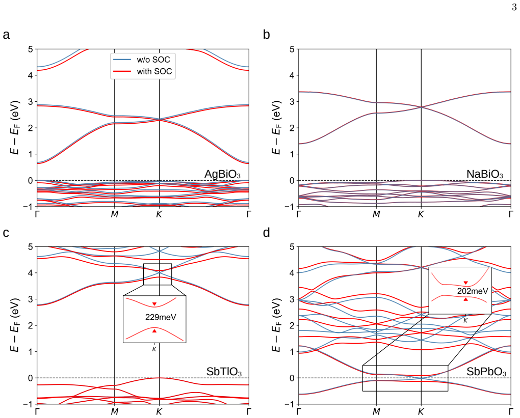
Spin-orbit coupling produces a 229 meV band inversion in SbTlO3 that remains topological after Pb substitution places the feature at the Fermi level.
A machine-rendered reading of the paper's core claim, the machinery that carries it, and where it could break.
Core claim
In SbTlO3 monolayers, inclusion of spin-orbit coupling opens a 229 meV gap at the bottom of the conduction bands accompanied by band inversion; the inverted character survives in SbPbO3 where the feature crosses the Fermi level. Topological invariants calculated for the 2D Brillouin zone and the appearance of protected edge states inside the gap for both zigzag and armchair ribbon terminations confirm the nontrivial topology of the splitting.
What carries the argument
SOC-driven band inversion in the monolayer oxides, diagnosed by Z2 invariants and by gap-crossing edge states on finite ribbons.
If this is right
- SbPbO3 monolayers are predicted to host a topologically protected 200 meV gap at the Fermi level.
- Both zigzag and armchair edges of the ribbons support conducting states inside the bulk gap.
- The same SOC mechanism can be explored systematically in other non-van der Waals 2D oxides containing heavy cations.
- The non-van der Waals bonding implies greater mechanical stability for device fabrication than conventional 2D TIs.
Where Pith is reading between the lines
- If the calculated gap survives substrate interactions and disorder, these materials could operate at room temperature where many van-der-Waals TIs do not.
- The surface-cation termination noted in the paper may allow electrostatic gating to move the Fermi level through the topological gap without destroying the inversion.
- Extending the substitutional tuning (Tl to Pb) to other isoelectronic replacements could map a larger family of non-vdW 2D TIs.
Load-bearing premise
Standard DFT plus spin-orbit coupling calculations on thin slabs give a reliable account of the size and topology of the gap without large errors from the choice of exchange-correlation functional or from missing electron correlation.
What would settle it
Angle-resolved photoemission or scanning tunneling spectroscopy on a grown SbPbO3 monolayer that fails to show the predicted edge states inside the 200 meV gap or that shows a topologically trivial band ordering.
Figures


read the original abstract
Non-van der Waals two-dimensional (2D) materials derived from strongly bonded non-layered crystals have recently emerged as a novel and rising platform for nanoscale research. While uncovering and tuning their (opto-)electronic, catalytic, and magnetic properties has been the focus of intense research, the impact of spin-orbit coupling (SOC) onto their electronic structure has not yet been explored in detail. Studying these effects is, however, particularly relevant due to their surface cation termination and the presence of heavy elements in several representative compounds. Here, we investigate the effect of SOC onto the electronic structure of 2D AgBiO3, NaBiO3, and SbTlO3. While the first two systems show negligible band renormalization upon inclusion of relativistic effects around the band gap, SbTlO3 showcases a large SOC induced splitting (229meV) for the lowest conduction bands associated with a band inversion. Substitution of Tl with Pb forming SbPbO3 brings the band-inverted feature to the Fermi level. Analysis of topological invariants and investigation of edge states of zig-zag and armchair ribbons within the 200meV gap confirms the topological nature of the band splitting. Our work thus establishes a foundation for the systematic study of robust non-van der Waals 2D topological insulators.
Editorial analysis
A structured set of objections, weighed in public.
Referee Report
Summary. The manuscript examines spin-orbit coupling (SOC) effects in non-van der Waals 2D materials AgBiO3, NaBiO3, SbTlO3, and SbPbO3 derived from bulk crystals. It reports negligible SOC impact on the first two compounds but a large 229 meV SOC-induced splitting and band inversion in SbTlO3, which is claimed to produce a non-trivial 2D topological insulator phase. This is supported by computed Z2 invariants and gapless edge states in zigzag and armchair ribbons inside the ~200 meV gap. SbPbO3 is shown to shift the inverted feature to the Fermi level. The work proposes these systems as a platform for studying robust non-vdW 2D topological insulators.
Significance. If the underlying calculations hold, the result would be significant for expanding 2D topological materials beyond van der Waals layered systems, particularly by leveraging heavy-element oxides with surface cation terminations to achieve sizable gaps. The combination of invariant calculations and explicit ribbon edge-state spectra provides a direct link between band inversion and topological protection, which is a strength relative to purely invariant-based claims.
major comments (3)
- [Abstract and Results on SbTlO3] Abstract and (presumed) Methods/Results sections: the central claim of a SOC-driven band inversion (229 meV) and non-trivial topology in SbTlO3 rests on DFT+SOC slab calculations, yet no exchange-correlation functional, k-point sampling, slab thickness, or convergence tests are specified. Semi-local functionals are known to mis-order bands or underestimate gaps in heavy-element oxides, directly undermining the reported splitting, Z2 value, and edge-state gaplessness.
- [Results on SbTlO3] Results on SbTlO3 and topological analysis: finite-thickness slab models can introduce spurious surface states or alter effective dimensionality and band inversion; without explicit thickness-convergence data or comparison to thicker slabs, the topological classification (Z2 invariants and 200 meV gap) cannot be considered robust.
- [Edge State Analysis] Edge-state investigation: the gapless states in zigzag and armchair ribbons are presented as confirmation of topology, but the manuscript provides no details on ribbon width, edge termination/pseudopotentials, or whether the states remain gapless under changes in functional or slab parameters. This is load-bearing for the claim that the splitting is topologically protected.
minor comments (2)
- [Abstract and Figures] Notation for the 229 meV splitting and 200 meV gap should be made consistent across text and figures to avoid reader confusion.
- [Methods] A brief statement on the software package and pseudopotentials used would improve reproducibility even before full methodological details are added.
Simulated Author's Rebuttal
We thank the referee for the constructive and detailed report. We address each major comment point by point below. Where the manuscript lacked sufficient detail, we have revised it to include the requested information and additional checks; we believe these changes strengthen the presentation without altering the central conclusions.
read point-by-point responses
-
Referee: [Abstract and Results on SbTlO3] Abstract and (presumed) Methods/Results sections: the central claim of a SOC-driven band inversion (229 meV) and non-trivial topology in SbTlO3 rests on DFT+SOC slab calculations, yet no exchange-correlation functional, k-point sampling, slab thickness, or convergence tests are specified. Semi-local functionals are known to mis-order bands or underestimate gaps in heavy-element oxides, directly undermining the reported splitting, Z2 value, and edge-state gaplessness.
Authors: We agree that the original manuscript omitted key methodological parameters. In the revised version we have added an explicit Methods section stating that all calculations employed the PBE functional with SOC, a 12×12×1 Γ-centered k-mesh for the 2D Brillouin zone, a four-layer slab with 20 Å vacuum, and projector-augmented-wave pseudopotentials. We also include a new supplementary figure demonstrating convergence of the 229 meV splitting to within 5 meV for slabs between three and six layers. While semi-local functionals can have limitations in heavy-element systems, the topological character is independently verified by the computed Z2 invariants and the presence of gapless edge states; these observables are less sensitive to the precise gap size than to the band-inversion topology itself. revision: yes
-
Referee: [Results on SbTlO3] Results on SbTlO3 and topological analysis: finite-thickness slab models can introduce spurious surface states or alter effective dimensionality and band inversion; without explicit thickness-convergence data or comparison to thicker slabs, the topological classification (Z2 invariants and 200 meV gap) cannot be considered robust.
Authors: We acknowledge that finite-slab artifacts must be ruled out. The revised manuscript now contains a thickness-convergence study (supplementary material) showing the band inversion and Z2 = 1 invariant for slabs from three to six layers; the ~200 meV gap stabilizes for thicknesses ≥4 layers and no spurious metallic surface states appear inside the gap. The edge-state calculations were performed on ribbons extracted from the converged four-layer slab, further reducing the likelihood of thickness-induced artifacts. revision: yes
-
Referee: [Edge State Analysis] Edge-state investigation: the gapless states in zigzag and armchair ribbons are presented as confirmation of topology, but the manuscript provides no details on ribbon width, edge termination/pseudopotentials, or whether the states remain gapless under changes in functional or slab parameters. This is load-bearing for the claim that the splitting is topologically protected.
Authors: We thank the referee for noting the missing technical specifications. The revised text now states that the ribbons are 30 unit cells wide, with edges terminated by hydrogen atoms using the same PAW potentials as the slab calculations. Additional tests (reported in the supplement) confirm that the edge states remain gapless inside the bulk gap when the ribbon width is increased to 40 unit cells and when a subset of configurations is recomputed with the HSE06 hybrid functional. These checks support that the gapless character is protected by the bulk topology rather than by specific numerical choices. revision: yes
Circularity Check
No circularity: standard DFT+SOC computations with independent topological checks
full rationale
The paper computes electronic bands via DFT+SOC, identifies a band inversion and 229 meV splitting in SbTlO3, then evaluates Z2 invariants and edge-state spectra in finite ribbons as independent verifications. None of these steps define the topological character in terms of itself, fit parameters to the target invariants, or rely on self-citations for uniqueness or ansatz. The derivation chain is self-contained and uses externally standard methods whose validity can be checked against other codes or functionals.
Axiom & Free-Parameter Ledger
axioms (2)
- domain assumption Standard density-functional theory plus spin-orbit coupling accurately describes the electronic structure near the gap in these oxides
- domain assumption Topological invariants computed from the DFT bands correctly classify the 2D system
Reference graph
Works this paper leans on
-
[1]
as well as hematene and ilmenene extracted from earth-abundant ores hematiteα-Fe 2O3 [8] and ilmenite FeTiO3 [9]. In the years following the discovery of the first rep- resentatives, numerous other systems were derived from non-vdW bonded compounds [10–20] by a variety of ex- perimental techniques [21, 22]. These investigations were also complemented by s...
work page internal anchor Pith review Pith/arXiv arXiv 2026
-
[3]
K. S. Novoselov, D. Jiang, F. Schedin, T. J. Booth, V. V. Khotkevich, S. V. Morozov, and A. K. Geim, Two-dimensional atomic crystals, Proceedings of the Na- tional Academy of Sciences102, 10451–10453 (2005), doi:10.1073/pnas.0502848102
-
[4]
V. Nicolosi, M. Chhowalla, M. G. Kanatzidis, M. S. Strano, and J. N. Coleman,Liquid Exfoliation of Layered Materials, Science340, 1226419 (2013), doi: 10.1126/science.1226419
-
[5]
Y. Huang, E. Sutter, N. N. Shi, J. Zheng, T. Yang, D. En- glund, H.-J. Gao, and P. Sutter,Reliable Exfoliation of Large-Area High-Quality Flakes of Graphene and Other Two-Dimensional Materials, ACS Nano9, 10612–10620 (2015), doi:10.1021/acsnano.5b04258
-
[6]
M. Velick´ y, P. S. Toth, A. M. Rakowski, A. P. Rooney, A. Kozikov, C. R. Woods, A. Mishchenko, L. Fumagalli, J. Yin, V. Z´ olyomi, T. Georgiou, S. J. Haigh, K. S. Novoselov, and R. A. W. Dryfe,Exfoliation of natu- ral van der Waals heterostructures to a single unit cell thickness, Nature Communications8, 14410 (2017), doi: 10.1038/ncomms14410
-
[7]
K. S. Novoselov, A. K. Geim, S. V. Morozov, D. Jiang, Y. Zhang, S. V. Dubonos, I. V. Grigorieva, and A. A. Firsov,Electric Field Effect in Atomically Thin Carbon Films, Science306, 666–669 (2004), doi: 10.1126/science.1102896
work page internal anchor Pith review doi:10.1126/science.1102896 2004
-
[8]
S. Manzeli, D. Ovchinnikov, D. Pasquier, O. V. Yazyev, and A. Kis,2D transition metal dichalco- genides, Nature Reviews Materials2, 17033 (2017), doi: 10.1038/natrevmats.2017.33
-
[9]
G. Guan, J. Xia, S. Liu, Y. Cheng, S. Bai, S. Y. Tee, Y.-W. Zhang, and M.-Y. Han,Electrostatic- Driven Exfoliation and Hybridization of 2D Nano- materials, Adv. Mater.29, 1700326 (2017), doi: 10.1002/adma.201700326
-
[10]
A. Puthirath Balan, S. Radhakrishnan, C. F. Woell- ner, S. K. Sinha, L. Deng, C. d. l. Reyes, B. M. Rao, M. Paulose, R. Neupane, A. Apte, V. Kochat, R. Va- jtai, A. R. Harutyunyan, C.-W. Chu, G. Costin, D. S. Galvao, A. A. Mart´ ı, P. A. van Aken, O. K. Varghese, C. S. Tiwary, A. Malie Madom Ramaswamy Iyer, and P. M. Ajayan,Exfoliation of a non-van der Wa...
-
[11]
A. Puthirath Balan, S. Radhakrishnan, R. Kumar, R. Ne- upane, S. K. Sinha, L. Deng, C. A. de los Reyes, A. Apte, B. M. Rao, M. Paulose, R. Vajtai, C. W. Chu, G. Costin, A. A. Mart´ ı, O. K. Varghese, A. K. Singh, C. S. Tiwary, M. R. Anantharaman, and P. M. Ajayan,A Non-van der Waals Two-Dimensional Material from Natural Ti- tanium Mineral Ore Ilmenite, Ch...
-
[12]
T. P. Yadav, S. N. Shirodkar, N. Lertcumfu, S. Radhakr- ishnan, F. N. Sayed, K. D. Malviya, G. Costin, R. Vajtai, B. I. Yakobson, C. S. Tiwary, and P. M. Ajayan,Chromi- teen: A New 2D Oxide Magnetic Material from Natural Ore, Advanced Materials Interfaces5, 1800549 (2018), doi:https://doi.org/10.1002/admi.201800549
-
[13]
A. B. Puthirath, S. N. Shirodkar, G. Gao, F. C. R. Hernandez, L. Deng, R. Dahal, A. Apte, G. Costin, 7 N. Chakingal, A. P. Balan, L. M. Sassi, C. S. Ti- wary, R. Vajtai, C.-W. Chu, B. I. Yakobson, and P. M. Ajayan,Scale-Enhanced Magnetism in Exfoliated Atom- ically Thin Magnetite Sheets, Small16, 2004208 (2020), doi:https://doi.org/10.1002/smll.202004208
-
[14]
H. Kaur, R. Tian, A. Roy, M. McCrystall, D. V. Horvath, G. Lozano Onrubia, R. Smith, M. Ruether, A. Griffin, C. Backes, V. Nicolosi, and J. N. Coleman,Production of Quasi-2D Platelets of Nonlayered Iron Pyrite (FeS 2) by Liquid-Phase Exfoliation for High Performance Bat- tery Electrodes, ACS Nano14, 13418–13432 (2020), doi: 10.1021/acsnano.0c05292
-
[15]
A. B. Puthirath, A. P. Balan, E. F. Oliveira, V. Sreepal, F. C. Robles Hernandez, G. Gao, N. Chakingal, L. M. Sassi, P. Thibeorchews, G. Costin, R. Vajtai, D. S. Gal- vao, R. R. Nair, and P. M. Ajayan,Apparent Ferromag- netism in Exfoliated Ultrathin Pyrite Sheets, The Journal of Physical Chemistry C125, 18927–18935 (2021), doi: 10.1021/acs.jpcc.1c04977
-
[16]
M. G. Moinuddin, S. Srinivasan, and S. K. Sharma,Prob- ing Ferrimagnetic Semiconductor with Enhanced Neg- ative Magnetoresistance: 2D Chromium Sulfide, Ad- vanced Electronic Materials7, 2001116 (2021), doi: https://doi.org/10.1002/aelm.202001116
-
[17]
L. Hu, L. Cao, L. Li, J. Duan, X. Liao, F. Long, J. Zhou, Y. Xiao, Y.-J. Zeng, and S. Zhou,Two-dimensional magneto-photoconductivity in non-van der Waals man- ganese selenide, Mater. Horiz.8, 1286–1296 (2021), doi: 10.1039/D1MH00009H
-
[18]
A. Yousaf, M. S. Gilliam, S. L. Y. Chang, M. Augustin, Y. Guo, F. Tahir, M. Wang, A. Schwindt, X. S. Chu, D. O. Li, S. Kale, A. Debnath, Y. Liu, M. D. Green, E. J. G. Santos, A. A. Green, and Q. H. Wang,Exfo- liation of Quasi-Two-Dimensional Nanosheets of Metal Diborides, The Journal of Physical Chemistry C125, 6787–6799 (2021), doi:10.1021/acs.jpcc.1c00394
-
[19]
Y. Guo, A. Gupta, M. S. Gilliam, A. Debnath, A. Yousaf, S. Saha, M. D. Levin, A. A. Green, A. K. Singh, and Q. H. Wang,Exfoliation of boron carbide into ultra- thin nanosheets, Nanoscale13, 1652–1662 (2021), doi: 10.1039/D0NR07971E
-
[20]
C. Gibaja, D. Rodr´ ıguez-San-Miguel, W. S. Paz, I. Tor- res, E. Salagre, P. Segovia, E. G. Michel, M. As- sebban, P. Ares, D. Hern´ andez-Maldonado, Q. Ra- masse, G. Abell´ an, J. G´ omez-Herrero, M. Varela, J. J. Palacios, and F. Zamora,Exfoliation of Alpha-Germanium: A Covalent Diamond-Like Struc- ture, Advanced Materials33, 2006826 (2021), doi: https:...
-
[21]
A. N. Toksumakov, G. A. Ermolaev, A. S. Slavich, N. V. Doroshina, E. V. Sukhanova, D. I. Yakubovsky, A. V. Syuy, S. M. Novikov, R. I. Romanov, A. M. Markeev, A. S. Oreshonkov, D. M. Tsymbarenko, Z. I. Popov, D. G. Kvashnin, A. A. Vyshnevyy, A. V. Arsenin, D. A. Ghazaryan, and V. S. Volkov,High-refractive index and mechanically cleavable non-van der Waals ...
-
[22]
K. Jiang, J. Ji, W. Gong, L. Ding, J. Li, P. Li, B. Li, and F. Geng,Mechanical cleavage of non-van der Waals structures towards two-dimensional crystals, Nat. Synth. 2, 58–66 (2023), doi:10.1038/s44160-022-00182-6
-
[23]
H. Kaur and J. N. Coleman,Liquid-Phase Exfolia- tion of Nonlayered Non-Van-Der-Waals Crystals into Nanoplatelets, Adv. Mater.34, 2202164 (2022), doi: 10.1002/adma.202202164
-
[24]
A. P. Balan, A. B. Puthirath, S. Roy, G. Costin, E. F. Oliveira, M. A. S. R. Saadi, V. Sreepal, R. Friedrich, P. Serles, A. Biswas, S. A. Iyengar, N. Chakingal, S. Bhattacharyya, S. K. Saju, S. C. Pardo, L. M. Sassi, T. Filleter, A. Krasheninnikov, D. S. Galvao, R. Vaj- tai, R. R. Nair, and P. M. Ajayan,Non-van der Waals quasi-2D materials; recent advance...
-
[25]
R. Friedrich, M. Ghorbani-Asl, S. Curtarolo, and A. V. Krasheninnikov,Data-Driven Quest for Two- Dimensional Non-van der Waals Materials, Nano Letters 22, 989–997 (2022), doi:10.1021/acs.nanolett.1c03841
-
[26]
T. Barnowsky, A. V. Krasheninnikov, and R. Friedrich, A New Group of 2D Non-van der Waals Ma- terials with Ultra Low Exfoliation Energies, Ad- vanced Electronic Materials9, 2201112 (2023), doi: https://doi.org/10.1002/aelm.202201112
-
[27]
M. Bagheri, E. Berger, and H.-P. Komsa,Identification of Material Dimensionality Based on Force Constant Anal- ysis, J. Phys. Chem. Lett.14, 7840–7847 (2023), doi: 10.1021/acs.jpclett.3c01635
-
[28]
Y. Hu, J. Jiang, P. Zhang, Z. Ma, F. Guan, D. Li, Z. Qian, X. Zhang, and P. Huang,Prediction of nonlay- ered oxide monolayers as flexible highi-κdielectrics with negative Poisson’s ratios, Nat. Commun.14, 6555 (2023), doi:10.1038/s41467-023-42312-4
-
[29]
Ono,Framework for identifying non–van der Waals two-dimensional materials, Phys
S. Ono,Framework for identifying non–van der Waals two-dimensional materials, Phys. Rev. B112, 075403 (2025), doi:10.1103/crw6-zvpx
-
[30]
Y. Zhong, Y. Xiao, Z. Qian, W. Xiong, and P. Huang, High-throughput exfoliation of multiferroic ternary ox- ide monolayers with high transition temperature and giant spin splitting, npj Comput. Mater. (2025), doi: 10.1038/s41524-025-01867-0
-
[31]
M. Bagheri, E. Berger, H.-P. Komsa, and P. Koskinen, Massive Discovery of Low-Dimensional Materials from Universal Computational Strategy, Chemistry of Materi- als (2026), doi:10.1021/acs.chemmater.5c03151
-
[32]
Barnowsky, C
T. Barnowsky, C. Timm, and R. Friedrich,Exfoliation and Cleavage of Crystals from a Universal Potential (2025)
2025
-
[33]
Y. Wei, M. Ghorbani-Asl, and A. V. Krashenin- nikov,Tailoring the Electronic and Magnetic Prop- erties of Hematene by Surface Passivation: Insights from First-Principles Calculations, The Journal of Physical Chemistry C124, 22784–22792 (2020), doi: 10.1021/acs.jpcc.0c05807
-
[34]
T. Barnowsky, S. Curtarolo, A. V. Krasheninnikov, T. Heine, and R. Friedrich,Magnetic State Con- trol of Non-van der Waals 2D Materials by Hydro- genation, Nano Letters24, 3874–3881 (2024), doi: 10.1021/acs.nanolett.3c04777
-
[35]
I. Tantis, S. Talande, V. Tzitzios, G. Basina, V. Shri- vastav, A. Bakandritsos, and R. Zboril,Non-van der Waals 2D Materials for Electrochemical Energy Storage, Advanced Functional Materials33, 2209360 (2023), doi: https://doi.org/10.1002/adfm.202209360
-
[36]
Nihei, T
A. Nihei, T. Barnowsky, and R. Friedrich,Non-van der Waals Heterostructures(2025)
2025
-
[37]
C. Jin and L. Kou,Two-dimensional non-van der Waals magnetic layers: functional materials for potential device 8 applications, Journal of Physics D: Applied Physics54, 413001 (2021), doi:10.1088/1361-6463/ac08ca
-
[38]
J. Mohapatra, A. Ramos, J. Elkins, J. Beatty, M. Xing, D. Singh, E. C. La Plante, and J. Ping Liu,Ferromag- netism in 2Dα-Fe2O3 nanosheets, Applied Physics Let- ters118, 183102 (2021), doi:10.1063/5.0045366
-
[39]
G. Giovannetti, P. A. Khomyakov, G. Brocks, V. M. Karpan, J. van den Brink, and P. J. Kelly,Doping Graphene with Metal Contacts, Phys. Rev. Lett.101, 026803 (2008), doi:10.1103/PhysRevLett.101.026803
-
[40]
C. Melios, A. Centeno, A. Zurutuza, V. Pan- chal, C. E. Giusca, S. Spencer, S. R. P. Silva, and O. Kazakova,Effects of humidity on the elec- tronic properties of graphene prepared by chemical vapour deposition, Carbon103, 273–280 (2016), doi: https://doi.org/10.1016/j.carbon.2016.03.018
-
[41]
J. D. Wood, S. A. Wells, D. Jariwala, K.-S. Chen, E. Cho, V. K. Sangwan, X. Liu, L. J. Lauhon, T. J. Marks, and M. C. Hersam,Effective Passivation of Ex- foliated Black Phosphorus Transistors against Ambient Degradation, Nano Letters14, 6964–6970 (2014), doi: 10.1021/nl5032293. PMID: 25380142
-
[42]
J. Kumar and M. Shrivastava,First-Principles Molecu- lar Dynamics Insight into the Atomic Level Degradation Pathway of Phosphorene, ACS Omega7, 696–704 (2022), doi:10.1021/acsomega.1c05353
-
[43]
Q. Li, Q. Zhou, L. Shi, Q. Chen, and J. Wang,Recent advances in oxidation and degradation mechanisms of ul- trathin 2D materials under ambient conditions and their passivation strategies, J. Mater. Chem. A7, 4291–4312 (2019), doi:10.1039/C8TA10306B
-
[44]
M. C. Lemme, D. Akinwande, C. Huyghebaert, and C. Stampfer,2D materials for future heterogeneous elec- tronics, Nature Communications13, 1392 (2022), doi: 10.1038/s41467-022-29001-4
-
[45]
L. Kou, Y. Ma, Z. Sun, T. Heine, and C. Chen, Two-Dimensional Topological Insulators: Progress and Prospects, The Journal of Physical Chemistry Letters8, 1905–1919 (2017), doi:10.1021/acs.jpclett.7b00222
-
[46]
G. Zhang, H. Wu, L. Zhang, L. Yang, Y. Xie, F. Guo, H. Li, B. Tao, G. Wang, W. Zhang, and H. Chang,Two-Dimensional Van Der Waals Topo- logical Materials: Preparation, Properties, and De- vice Applications, Small18, 2204380 (2022), doi: https://doi.org/10.1002/smll.202204380
-
[47]
B. Weber, M. S. Fuhrer, X.-L. Sheng, S. A. Yang, R. Thomale, S. Shamim, L. W. Molenkamp, D. Cobden, D. Pesin, H. J. W. Zandvliet, P. Bampoulis, R. Claessen, F. R. Menges, J. Gooth, C. Felser, C. Shekhar, A. Tadich, M. Zhao, M. T. Edmonds, J. Jia, M. Bieniek, J. I. V¨ ayrynen, D. Culcer, B. Muralidharan, and M. Nadeem, 2024 roadmap on 2D topological insula...
-
[48]
Z. Zhu, Y. Cheng, and U. Schwingenschl¨ ogl,Band in- version mechanism in topological insulators: A guideline for materials design, Phys. Rev. B85, 235401 (2012), doi:10.1103/PhysRevB.85.235401
-
[49]
J. Vidal, X. Zhang, V. Stevanovi´ c, J.-W. Luo, and A. Zunger,Large insulating gap in topological insulators induced by negative spin-orbit splitting, Phys. Rev. B86, 075316 (2012), doi:10.1103/PhysRevB.86.075316
-
[50]
J. G. Analytis, R. D. McDonald, S. C. Riggs, J.- H. Chu, G. S. Boebinger, and I. R. Fisher,Two- dimensional surface state in the quantum limit of a topo- logical insulator, Nature Physics6, 960–964 (2010), doi: 10.1038/nphys1861
-
[51]
F. Zhang, C. L. Kane, and E. J. Mele,Surface states of topological insulators, Phys. Rev. B86, 081303 (2012), doi:10.1103/PhysRevB.86.081303
-
[52]
K. Zhang, H. V. Lepage, Y. Dong, and C. H. W. Barnes,Charge qubits based on ultra-thin topological in- sulator films, Frontiers of Physics19, 33208 (2023), doi: 10.1007/s11467-023-1364-5
-
[53]
Q. Yan, H. Li, H. Jiang, Q.-F. Sun, and X. C. Xie, Rules for dissipationless topotronics, Science Advances 10, eado4756 (2024), doi:10.1126/sciadv.ado4756. [52]The FLEUR project,https://www.flapw.de/(2024)
-
[54]
D. Wortmann, G. Michalicek, N. Baadji, M. Bet- zinger, G. Bihlmayer, J. Br¨ oder, T. Burnus, J. Enko- vaara, F. Freimuth, C. Friedrich, C.-R. Gerhorst, S. Granberg Cauchi, U. Grytsiuk, A. Hanke, J.-P. Hanke, M. Heide, S. Heinze, R. Hilgers, H. Janssen, D. A. Kl¨ uppelberg, R. Kovacik, P. Kurz, M. Lezaic, G. K. H. Madsen, Y. Mokrousov, A. Neukirchen, M. Re...
-
[55]
S. P. Huber, S. Zoupanos, M. Uhrin, L. Talirz, L. Kahle, R. H¨ auselmann, D. Gresch, T. M¨ uller, A. V. Yaku- tovich, C. W. Andersen, F. F. Ramirez, C. S. Adorf, F. Gargiulo, S. Kumbhar, E. Passaro, C. Johnston, A. Merkys, A. Cepellotti, N. Mounet, N. Marzari, B. Kozinsky, and G. Pizzi,AiiDA 1.0, a scalable compu- tational infrastructure for automated rep...
-
[56]
M. Uhrin, S. P. P. Huber, J. Yu, N. Marzari, and G. Pizzi, Workflows in AiiDA: Engineering a high-throughput, event-based engine for robust and modular computational workflows, Computational Materials Science187, 110086 (2021), doi:10.1016/j.commatsci.2020.110086
-
[57]
C. Oses, M. Esters, D. Hicks, S. Divilov, H. Eckert, R. Friedrich, M. J. Mehl, A. Smolyanyuk, X. Campi- longo, A. van de Walle, J. Schroers, A. G. Kusne, I. Takeuchi, E. Zurek, M. B. Nardelli, M. Fornari, Y. Led- erer, O. Levy, C. Toher, and S. Curtarolo,aflow++: A C++ framework for autonomous materials design, Com- putational Materials Science217, 111889...
-
[58]
M. Esters, C. Oses, S. Divilov, H. Eckert, R. Friedrich, D. Hicks, M. J. Mehl, F. Rose, A. Smolyanyuk, A. Cal- zolari, X. Campilongo, C. Toher, and S. Curtarolo, aflow.org: A web ecosystem of databases, software and tools, Computational Materials Science216, 111808 (2023), doi:10.1016/j.commatsci.2022.111808
-
[59]
S. Divilov, H. Eckert, S. D. Thiel, S. D. Griesemer, R. Friedrich, N. H. Anderson, M. J. Mehl, D. Hicks, M. Esters, N. Hotz, X. Campilongo, A. Calzolari, and S. Curtarolo,AFLOW4: Heading Toward Disorder, High Entropy Alloys Mater.3, 178–187 (2025), doi: 10.1007/s44210-025-00058-2
-
[60]
Physical Review B47, 558–561 (1993)
G. Kresse and J. Hafner,Ab initio molecular dynamics for liquid metals, Phys. Rev. B47, 558–561 (1993), doi: 10.1103/PhysRevB.47.558
-
[61]
G. Kresse and J. Furthm¨ uller,Efficient iterative schemes for ab initio total-energy calculations using a plane-wave basis set, Phys. Rev. B54, 11169–11186 (1996), doi: 9 10.1103/PhysRevB.54.11169
-
[62]
G. Kresse and J. Furthm¨ uller,Efficiency of ab-initio to- tal energy calculations for metals and semiconductors us- ing a plane-wave basis set, Computational Materials Sci- ence6, 15–50 (1996), doi:https://doi.org/10.1016/0927- 0256(96)00008-0
-
[63]
C. E. Calderon, J. J. Plata, C. Toher, C. Oses, O. Levy, M. Fornari, A. Natan, M. J. Mehl, G. Hart, M. Buon- giorno Nardelli, and S. Curtarolo,The AFLOW standard for high-throughput materials science calculations, Com- putational Materials Science108, 233–238 (2015), doi: https://doi.org/10.1016/j.commatsci.2015.07.019
-
[64]
H. Krakauer, M. Posternak, and A. J. Freeman,Lin- earized augmented plane-wave method for the electronic band structure of thin films, Phys. Rev. B19, 1706–1719 (1979), doi:10.1103/PhysRevB.19.1706
-
[65]
A. A. Mostofi, J. R. Yates, G. Pizzi, Y.-S. Lee, I. Souza, D. Vanderbilt, and N. Marzari,An up- dated version of wannier90: A tool for obtain- ing maximally-localised Wannier functions, Computer Physics Communications185, 2309–2310 (2014), doi: https://doi.org/10.1016/j.cpc.2014.05.003
-
[66]
Q. Wu, S. Zhang, H.-F. Song, M. Troyer, and A. A. Soluyanov,WannierTools: An open-source soft- ware package for novel topological materials, Computer Physics Communications224, 405–416 (2018), doi: https://doi.org/10.1016/j.cpc.2017.09.033
-
[67]
S.-M. Jeong, S. Yi, H.-J. Kim, G. Bihlmayer, and J.-H. Cho,Competing edge structures of Sb and Bi bilayers generated by trivial and nontrivial band topologies, Phys. Rev. B98, 075402 (2018), doi: 10.1103/PhysRevB.98.075402
-
[68]
M. Lokamani, G. Bihlmayer, G. Michalicek, D. Wort- mann, S. Bl¨ ugel, and R. Friedrich,Data Publication: To- wards Non-van der Waals 2D Topological Insulators, Ro- dare (2026), doi:10.14278/rodare.4591
discussion (0)
Sign in with ORCID, Apple, or X to comment. Anyone can read and Pith papers without signing in.