Recognition: unknown
Gradient Residual Stress in Transferred Thin-Film Lithium Niobate and Its Compenstation Using Periodically Poled Piezoelectric Bilayers
Pith reviewed 2026-05-09 22:28 UTC · model grok-4.3
The pith
Transferred thin-film lithium niobate films carry a residual stress gradient that varies with crystal orientation and thickness and can be partially cancelled by bilayers of opposite orientation.
A machine-rendered reading of the paper's core claim, the machinery that carries it, and where it could break.
Core claim
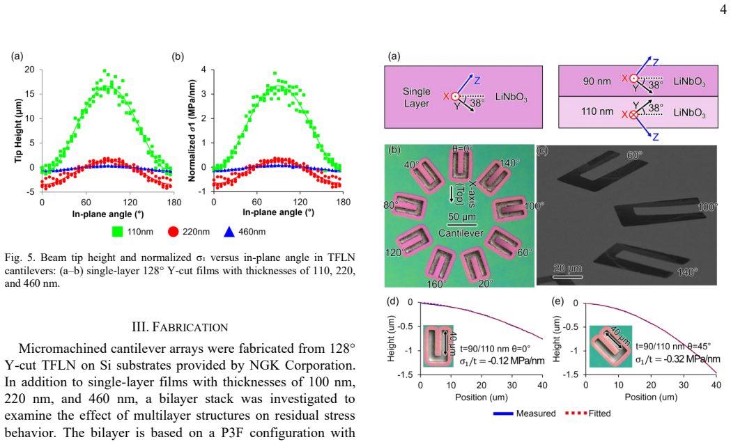
In 128 deg Y-cut transferred TFLN the normalized gradient stress sigma1 reaches 3.4 MPa/nm in 100 nm films and falls with thickness, with near-zero-gradient orientations near 55 and 125 degrees for 220-460 nm films but shifting to 20 and 160 degrees for 100 nm films. Finite element simulations confirm the gradient arises from orientation-dependent residual stress. A 90/110 nm bilayer with opposite orientations reduces the effective gradient to -0.4 to -0.04 MPa/nm and markedly lowers cantilever deformation.
What carries the argument
Cantilever curvature measurement used to extract the normalized residual stress gradient sigma1, together with periodically poled piezoelectric film (P3F) bilayers formed from two TFLN layers of opposite crystallographic orientation that partially cancel the gradient.
Load-bearing premise
Cantilever curvature directly and exclusively reflects the film's internal through-thickness stress gradient without significant contributions from bonding interfaces or transfer artifacts.
What would settle it
Depth-resolved stress mapping, for example by x-ray diffraction or Raman spectroscopy through the film thickness on the same low-curvature samples, would show whether the extracted gradient is truly near zero.
Figures


read the original abstract
In this work, we experimentally investigate the gradient stress (sigma1) in 128 deg Y-cut transferred thin film lithium niobate (TFLN) films with thicknesses from 100 to 460 nm using cantilever curvature analysis. The results reveal a strong dependence of sigma1 on both crystallographic orientation and film thickness, with stress-free orientations at approximately 55 deg and 125 deg for 220-460 nm films, shifting to approximately 20 deg and 160 deg for 100 nm films. The extracted normalized sigma1 ranges from -0.1 to 3.4 MPa/nm (100 nm), -0.8 to 0.34 MPa/nm (220 nm), and -0.12 to 0.08 MPa/nm (460 nm), indicating a pronounced thickness-dependent through-thickness stress gradient. Finite element simulations show excellent agreement with the measurements, validating the curvature-based extraction method and confirming that sigma1 originates from an orientation-dependent residual stress gradient. To mitigate this effect, a bilayer TFLN structure with opposite crystallographic orientations, forming a periodically poled piezoelectric film (P3F), is investigated, enabling partial cancellation of sigma1. A 90/110 nm P3F bilayer reduces the equivalent normalized sigma1 to -0.4 to -0.04 MPa/nm, resulting in significantly reduced deformation. These results establish gradient stress engineering through orientation, thickness, and bilayer design as an effective strategy for achieving mechanically stable and scalable TFLN microelectromechanical systems (MEMS) devices.
Editorial analysis
A structured set of objections, weighed in public.
Referee Report
Summary. The manuscript experimentally investigates the through-thickness residual stress gradient (σ₁) in transferred 128° Y-cut TFLN films (100–460 nm thick) via cantilever curvature analysis, reporting strong dependence on crystallographic orientation and thickness with stress-free angles shifting from ~55°/125° (thicker films) to ~20°/160° (100 nm films). Normalized σ₁ values decrease with increasing thickness, finite-element simulations show agreement with measurements, and a periodically poled piezoelectric bilayer (P3F) with opposite orientations is shown to reduce effective σ₁ (e.g., 90/110 nm bilayer yields –0.4 to –0.04 MPa/nm).
Significance. If the curvature-to-stress mapping is validated, the results demonstrate a viable engineering approach for mitigating deformation in TFLN MEMS through orientation, thickness, and bilayer design, supporting scalability. The experimental-simulation agreement is a strength, though its value depends on model completeness and experimental controls.
major comments (2)
- [Methods] Methods (curvature analysis description): The extraction of normalized σ₁ from cantilever curvature assumes observed deflection reports exclusively the intrinsic through-thickness stress gradient. No controls, subtraction procedures, or discussion address possible contributions from interface bonding, transfer-process artifacts, or interfacial compliance, which directly undermines the reported orientation dependence, thickness scaling, and bilayer cancellation efficacy.
- [Abstract/Results] Abstract and Results (reported stress values): Specific normalized σ₁ ranges (e.g., –0.1 to 3.4 MPa/nm for 100 nm films) and claims of 'excellent agreement' with FE simulations are given without error bars, sample statistics, reproducibility details, or data-exclusion criteria, preventing assessment of whether measurements robustly support the central claims on gradient engineering.
minor comments (1)
- [Abstract] The abstract states the bilayer 'results in significantly reduced deformation' but provides no quantitative comparison of curvature or deflection before/after compensation.
Simulated Author's Rebuttal
We thank the referee for the constructive and detailed review of our manuscript on gradient residual stress in transferred thin-film lithium niobate. The comments highlight important aspects of methodological transparency and statistical reporting that we will address in revision. Below we respond point by point to the major comments.
read point-by-point responses
-
Referee: [Methods] Methods (curvature analysis description): The extraction of normalized σ₁ from cantilever curvature assumes observed deflection reports exclusively the intrinsic through-thickness stress gradient. No controls, subtraction procedures, or discussion address possible contributions from interface bonding, transfer-process artifacts, or interfacial compliance, which directly undermines the reported orientation dependence, thickness scaling, and bilayer cancellation efficacy.
Authors: We agree that the curvature analysis relies on the assumption that deflection is dominated by the film's intrinsic stress gradient, and that explicit discussion of potential interface contributions was insufficient. The orientation dependence and thickness scaling we observe are difficult to attribute to isotropic interface or transfer artifacts, as these would not produce the systematic shifts in stress-free angles or the specific bilayer cancellation we demonstrate. The finite-element simulations, which model only the film stress gradient, also match the data closely. In the revised manuscript we will expand the Methods and/or Discussion sections with a dedicated paragraph on possible confounding factors (interface bonding, transfer artifacts, interfacial compliance), explaining why they are unlikely to dominate based on the crystallographic specificity of the results and the bilayer behavior. We cannot retroactively add new experimental controls or subtraction procedures, but the added discussion will make the assumptions and supporting evidence more transparent. revision: partial
-
Referee: [Abstract/Results] Abstract and Results (reported stress values): Specific normalized σ₁ ranges (e.g., –0.1 to 3.4 MPa/nm for 100 nm films) and claims of 'excellent agreement' with FE simulations are given without error bars, sample statistics, reproducibility details, or data-exclusion criteria, preventing assessment of whether measurements robustly support the central claims on gradient engineering.
Authors: We appreciate this point on statistical transparency. The reported ranges reflect the variation across crystallographic orientations for each thickness, obtained from repeated cantilever measurements. In the revised manuscript we will update the Abstract and Results to include error bars (standard deviation or standard error) on the normalized σ₁ values, state the number of independent samples per condition, and add a short description of reproducibility and data-exclusion criteria (e.g., exclusion of visibly damaged cantilevers). The agreement with finite-element simulations will be quantified (for example via RMS deviation between measured and simulated curvatures) rather than described only qualitatively. These changes will allow readers to evaluate the robustness of the gradient-engineering claims more directly. revision: yes
Circularity Check
No significant circularity; experimental extraction and FE validation remain independent
full rationale
The paper's core chain consists of direct cantilever curvature measurements on transferred TFLN films of varying thickness and orientation, followed by extraction of normalized residual stress gradient σ₁ using standard curvature-to-stress relations. Finite-element simulations are then used to confirm consistency with the measured curvatures under the same physical assumptions, but this does not constitute a fitted-input prediction loop because the FE model incorporates the independently measured geometry, material properties, and orientation dependence rather than re-using the extracted σ₁ values as the sole input to reproduce the identical data set. Bilayer compensation is likewise shown by direct fabrication and re-measurement of reduced curvature, not by algebraic rearrangement of the original extraction equations. No self-citations, ansatzes, or uniqueness theorems are invoked to close the derivation; the results are therefore self-contained against external benchmarks.
Axiom & Free-Parameter Ledger
axioms (2)
- domain assumption Cantilever curvature analysis via established thin-film formulas accurately isolates the through-thickness stress gradient sigma1
- domain assumption Finite element model of the bilayer correctly predicts stress cancellation without unmodeled interface or fabrication effects
Reference graph
Works this paper leans on
-
[1]
Mechanical behaviour of metallic thin films on polymeric substrates and the effect of ion beam assistance on crack propagation,
M. George, C. Coupeau, J. Colin, and J. Grilhé, “Mechanical behaviour of metallic thin films on polymeric substrates and the effect of ion beam assistance on crack propagation,” Acta Mater., vol. 53, no. 2, pp. 411 – 417, 2005
2005
-
[2]
A. D. Romig, M. T. Dugger, and P. J. McWhorter, “Materials issues in microelectromechanical devices: science, engineering, manufacturability and reliability,” Acta Mater. , vol. 51, no. 19, pp. 5837–5866, Nov. 2003, doi: 10.1016/S1359-6454(03)00440-3
-
[3]
How soft substrates affect the buckling delamination of thin films through crack front sink - in,
R. Boijoux, G. Parry, J.-Y. Faou, and C. Coupeau, “How soft substrates affect the buckling delamination of thin films through crack front sink - in,” Appl. Phys. Lett. , vol. 110, no. 14, p. 141602, Apr. 2017, doi: 10.1063/1.4979614
-
[4]
From telephone cords to branched buckles: A phase diagram,
J.-Y. Faou, S. Grachev, E. Barthel, and G. Parry, “From telephone cords to branched buckles: A phase diagram,” Acta Mater., vol. 125, pp. 524– 531, Feb. 2017, doi: 10.1016/j.actamat.2016.12.025
-
[5]
Post buckling of micromachined beams,
W. Fang and J. A. Wickert, “Post buckling of micromachined beams,” J. Micromechanics Microengineering , vol. 4, no. 3, p. 116, Sep. 1994, doi: 10.1088/0960-1317/4/3/004
-
[6]
S. Djaziri et al. , “Comparative study of the mechanical properties of nanostructured thin films on stretchable substrates,” J. Appl. Phys., vol. 116, no. 9, p. 093504, Sep. 2014, doi: 10.1063/1.4894616
-
[7]
A methodology for determining mechanical properties of freestanding thin films and MEMS materials,
H. D. Espinosa, B. C. Prorok, and M. Fischer, “A methodology for determining mechanical properties of freestanding thin films and MEMS materials,” J. Mech. Phys. Solids, vol. 51, no. 1, pp. 47 –67, Jan. 2003, doi: 10.1016/S0022-5096(02)00062-5
-
[8]
Enhanced Proton Conductivity in Y -Doped BaZrO3 via Strain Engineering,
A. Fluri et al., “Enhanced Proton Conductivity in Y -Doped BaZrO3 via Strain Engineering,” Adv. Sci. , vol. 4, no. 12, p. 1700467, 2017, doi: 10.1002/advs.201700467
-
[9]
Growth stress induced tunability of dielectric permittivity in thin films,
K. V. L. V. Narayanachari et al., “Growth stress induced tunability of dielectric permittivity in thin films,” J. Appl. Phys. , vol. 119, no. 1, p. 014106, Jan. 2016, doi: 10.1063/1.4939466
-
[10]
X. Yu, Y. Hou, M. Zheng, and M. Zhu, “Stress Engineering of Perovskite Ceramics for Enhanced Piezoelectricity and Temperature Stability toward Energy Harvesting,” ACS Appl. Electron. Mater. , vol. 4, no. 3, pp. 1359–1366, Mar. 2022, doi: 10.1021/acsaelm.2c00135
-
[11]
The correlation between mechanical stress and magnetic anisotropy in ultrathin films,
D. Sander, “The correlation between mechanical stress and magnetic anisotropy in ultrathin films,” Rep. Prog. Phys. , vol. 62, no. 5, p. 809, May 1999, doi: 10.1088/0034-4885/62/5/204
-
[12]
On the geometry design of AlN Lamb wave resonators with predefined shallow release cavities,
T.-H. Hsu et al. , “On the geometry design of AlN Lamb wave resonators with predefined shallow release cavities,” in Proc. Solid - State Sensor, Actuator, Microsyst. Workshop (Hilton Head) , 2022, pp. 1–62. Accessed: Nov. 10, 2025. foundation.org/technical_digests/HiltonHead_2022/hh2022_0210.pdf
2022
-
[13]
5 Ghz lithium niobate MEMS resonators with high FoM of 153,
Y. Yang, A. Gao, R. Lu, and S. Gong, “5 Ghz lithium niobate MEMS resonators with high FoM of 153,” in 2017 IEEE 30th International Conference on Micro Electro Mechanical Systems (MEMS) , Jan. 2017, pp. 942–945. doi: 10.1109/MEMSYS.2017.7863565
-
[14]
R. Lu, “Recent advances in high-performance millimeter-Wave acoustic resonators and filters using thin -film lithium niobate,” Prog. Quantum Electron., vol. 100 –101, p. 100565, 2025, doi: https://doi.org/10.1016/j.pquantelec.2025.100565
-
[15]
Applications of thin -film lithium niobate in nonlinear integrated photonics,
M. G. Vazimali and S. Fathpour, “Applications of thin -film lithium niobate in nonlinear integrated photonics,” Adv. Photonics, vol. 4, no. 3, pp. 034001–034001, 2022
2022
-
[16]
Optical nonlinearity of thin film lithium niobate: devices and recent progress,
L. Wang, H. Du, X. Zhang, and F. Chen, “Optical nonlinearity of thin film lithium niobate: devices and recent progress,” J. Phys. Appl. Phys., vol. 58, no. 2, p. 023001, Oct. 2024, doi: 10.1088/1361-6463/ad7ff7
-
[17]
Dual -Axis MEMS Resonant Scanner Using 128∘Y Lithium Niobate Thin -Film,
Y. Lu, K. Liu, and T. Wu, “Dual -Axis MEMS Resonant Scanner Using 128∘Y Lithium Niobate Thin -Film,” Acoustics, vol. 4, no. 2, pp. 313 – 328, Apr. 2022, doi: 10.3390/acoustics4020019
-
[18]
H. Wei et al., “High-Performance Piezoelectric-Type MEMS Vibration Sensor Based on LiNbO3 Single -Crystal Cantilever Beams,” Micromachines, vol. 13, no. 2, p. 329, Feb. 2022, doi: 10.3390/mi13020329
-
[19]
G. Clementi et al. , “LiNbO3 films – A low -cost alternative lead -free piezoelectric material for vibrational energy harvesters,” Mech. Syst. Signal Process. , vol. 149, p. 107171, Feb. 2021, doi: 10.1016/j.ymssp.2020.107171
-
[20]
Nanophotonic waveguide chip -to-world beam scanning,
M. Saha et al. , “Nanophotonic waveguide chip -to-world beam scanning,” Nature, vol. 651, no. 8105, pp. 356–363, 2026
2026
-
[21]
Thickness dependent stresses and thermal expansion of epitaxial LiNbO3 thin films on C-sapphire,
A. Bartasyte et al. , “Thickness dependent stresses and thermal expansion of epitaxial LiNbO3 thin films on C-sapphire,” Mater. Chem. Phys., vol. 149 –150, pp. 622 –631, Jan. 2015, doi: 10.1016/j.matchemphys.2014.11.018
-
[22]
R. Takigawa, T. Tomimatsu, E. Higurashi, and T. Asano, “Residual Stress in Lithium Niobate Film Layer of LNOI/Si Hybrid Wafer Fabricated Using Low-Temperature Bonding Method,” Micromachines, vol. 10, no. 2, p. 136, Feb. 2019, doi: 10.3390/mi10020136
-
[23]
K. Prabhakar, R. J. Patton, and R. M. Reano, “Stress reduction and wafer bow accommodation for the fabrication of thin film lithium niobate on oxidized silicon,” J. Vac. Sci. Technol. B Nanotechnol. Microelectron. Mater. Process. Meas. Phenom. , vol. 39, no. 6, p. 062208, Dec. 2021, doi: 10.1116/6.0001283
-
[24]
Residual Stress Anisotropy in Thin -Film Lithium Niobate for Stress -Managed Mems,
B. Kim et al. , “Residual Stress Anisotropy in Thin -Film Lithium Niobate for Stress -Managed Mems,” in 2026 IEEE 39th International Conference on Micro Electro Mechanical Systems (MEMS) , Jan. 2026, pp. 1352–1355. doi: 10.1109/MEMS64181.2026.11419544
-
[25]
S. Cho et al. , “23.8 -GHz Acoustic Filter in Periodically Poled Piezoelectric Film Lithium Niobate With 1.52-dB IL and 19.4% FBW,” IEEE Microw. Wirel. Technol. Lett. , vol. 34, no. 4, pp. 391 –394, Apr. 2024, doi: 10.1109/LMWT.2024.3368354
-
[26]
J. Zheng, Z. Ren, J. Xu, X. Liu, F. Qian, and Y. Yang, “Periodically Poled Piezoelectric Single -Layered and Multilayered Lithium Niobate for Thickened High-Order Lamb Wave Acoustic Devices,” IEEE Trans. Microw. Theory Tech. , vol. 73, no. 10, pp. 7069 –7079, Oct. 2025, doi: 10.1109/TMTT.2025.3567329
-
[27]
Determining mean and gradient residual stresses in thin films using micromachined cantilevers,
W. Fang and J. A. Wickert, “Determining mean and gradient residual stresses in thin films using micromachined cantilevers,” J. Micromechanics Microengineering , vol. 6, no. 3, pp. 301 –309, Sep. 1996, doi: 10.1088/0960-1317/6/3/002
-
[28]
L. B. Freund and S. Suresh, Thin film materials: stress, defect formation and surface evolution . Cambridge university press, 2004. Accessed: Mar. 23, 2026
2004
-
[29]
On the thermal expansion coefficients of thin films,
W. Fang and C. -Y. Lo, “On the thermal expansion coefficients of thin films,” Sens. Actuators Phys. , vol. 84, no. 3, pp. 310 –314, Sep. 2000, doi: 10.1016/S0924-4247(00)00311-3
-
[30]
Review Article: Stress in thin films and coatings: Current status, challenges, and prospects,
G. Abadias et al. , “Review Article: Stress in thin films and coatings: Current status, challenges, and prospects,” J. Vac. Sci. Technol. A , vol. 36, no. 2, p. 020801, Mar. 2018, doi: 10.1116/1.5011790
-
[31]
R. Treml et al., “High resolution determination of local residual stress gradients in single- and multilayer thin film systems,” Acta Mater., vol. 103, pp. 616–623, Jan. 2016, doi: 10.1016/j.actamat.2015.10.044
-
[32]
X. Xu, T. -C. Chong, S. Solanki, X. Liang, and S. Yuan, “Anisotropic thermal expansion of stoichiometric lithium niobate crystals grown along the normal direction of facets,” Opt. Mater. , vol. 26, no. 4, pp. 489–494, Sep. 2004, doi: 10.1016/j.optmat.2003.12.027
-
[33]
Residual stresses and clamped thermal expansion in LiNbO3 and LiTaO3 thin films,
A. Bartasyte et al., “Residual stresses and clamped thermal expansion in LiNbO3 and LiTaO3 thin films,” Appl. Phys. Lett. , vol. 101, no. 12, p. 122902, Sep. 2012, doi: 10.1063/1.4752448
-
[34]
Theory of plates and shells,
S. Timoshenko and S. Woinowsky -Krieger, “Theory of plates and shells,” 1959, Accessed: Mar. 23, 2026
1959
-
[35]
A. H. Fahmy and E. L. Adler, “Computer -program description. Transformation of tensor constants of anisotropic materials due to 8 rotations of the co-ordinate axes,” Proc. Inst. Electr. Eng., vol. 122, no. 5, pp. 591–592, May 1975, doi: 10.1049/piee.1975.0163
-
[36]
Anisotropic elasticity of silicon and its application to the modelling of X-ray optics,
L. Zhang, R. Barrett, P. Cloetens, C. Detlefs, and M. Sanchez del Rio, “Anisotropic elasticity of silicon and its application to the modelling of X-ray optics,” J. Synchrotron Radiat., vol. 21, no. 3, pp. 507 –517, May 2014, doi: 10.1107/S1600577514004962
-
[37]
M. Stefenelli et al., “X-ray analysis of residual stress gradients in TiN coatings by a Laplace space approach and cross -sectional nanodiffraction: a critical comparison,” J. Appl. Crystallogr. , vol. 46, no. 5, pp. 1378–1385, Oct. 2013, doi: 10.1107/S0021889813019535
-
[38]
A. Zeilinger et al. , “In -situ Observation of Cross -Sectional Microstructural Changes and Stress Distributions in Fracturing TiN Thin Film during Nanoindentation,” Sci. Rep., vol. 6, no. 1, p. 22670, Mar. 2016, doi: 10.1038/srep22670
-
[39]
A. M. Korsunsky, M. Sebastiani, and E. Bemporad, “Residual stress evaluation at the micrometer scale: Analysis of thin coatings by FIB milling and digital image correlation,” Surf. Coat. Technol. , vol. 205, no. 7, pp. 2393–2403, Dec. 2010, doi: 10.1016/j.surfcoat.2010.09.033
-
[40]
M. Huff, “Review Paper: Residual Stresses in Deposited Thin -Film Material Layers for Micro - and Nano -Systems Manufacturing,” Micromachines, vol. 13, no. 12, p. 2084, Nov. 2022, doi: 10.3390/mi13122084
-
[41]
A Generalized Acoustic Framework for Multilayer Piezoelectric Platforms,
J. Kramer and R. Lu, “A Generalized Acoustic Framework for Multilayer Piezoelectric Platforms,” IEEE Trans. Ultrason. Ferroelectr. Freq. Control , vol. 72, no. 9, pp. 1302 –1311, Sep. 2025, doi: 10.1109/TUFFC.2025.3595433
-
[42]
R. Lu, Y. Yang, S. Link, and S. Gong, “Enabling Higher Order Lamb Wave Acoustic Devices With Complementarily Oriented Piezoelectric Thin Films,” J. Microelectromechanical Syst., vol. 29, no. 5, pp. 1332 – 1346, Oct. 2020, doi: 10.1109/JMEMS.2020.3007590
-
[43]
Twist piezoelectricity: giant electromechanical coupling in magic-angle twisted bilayer LiNbO3,
H. Yao et al., “Twist piezoelectricity: giant electromechanical coupling in magic-angle twisted bilayer LiNbO3,” Nat. Commun., vol. 15, no. 1, p. 5002, Jun. 2024, doi: 10.1038/s41467-024-49321-x
-
[44]
Z.-H. Qin et al. , “Double -layer LiNbO3 longitudinally excited shear wave resonators with ultra -large electromechanical coupling coefficient and spurious-free performance,” Appl. Phys. Lett., vol. 126, no. 19, May 2025, doi: 10.1063/5.0250773
-
[45]
Thermal expansion of lithium tantalate an lithium niobate single crystals,
Y. S. Kim and R. T. Smith, “Thermal Expansion of Lithium Tantalate and Lithium Niobate Single Crystals,” J. Appl. Phys. , vol. 40, no. 11, pp. 4637–4641, Oct. 1969, doi: 10.1063/1.1657244
-
[46]
W. M. Yim and R. J. Paff, “Thermal expansion of AlN, sapphire, and silicon,” J. Appl. Phys. , vol. 45, no. 3, pp. 1456 –1457, Mar. 1974, doi: 10.1063/1.1663432. BYEONGJIN KIM (Student Member, IEEE) received the B.S. degree in applied physics from Korea Military Academy, Seoul, South Korea , in 2019 . He is currently pursuing the M.S. degree in Electrical ...
-
[47]
His research focuses on the development of advanced piezoelectric RF acoustic devices targeting the next generation wireless signal processing . He received the Scholarship Pilot Program to Cultivate Outstanding Doctoral Students from Ministry of Science and Technology of Taiwan in 2020 , the CTCI Foundation Science and Technology Research Scholarship in ...
2020
discussion (0)
Sign in with ORCID, Apple, or X to comment. Anyone can read and Pith papers without signing in.