Recognition: unknown
Nonvolatile single-ion memory with picosecond switching
Pith reviewed 2026-05-10 16:03 UTC · model grok-4.3
The pith
Single-ion movement through atomic vacancies in boron nitride enables nonvolatile memory with 20-picosecond switching and 310 attojoule energy use.
A machine-rendered reading of the paper's core claim, the machinery that carries it, and where it could break.
Core claim
Trapping and releasing one ion across the boron-nitride plane at a single-atom vacancy produces two distinct, stable resistance states that function as nonvolatile memory bits, with the short travel distance yielding 20 ps switching and 310 aJ/bit energy consumption.
What carries the argument
Single-ion penetration across the BN plane at vacancy defects, where capture or release of one ion toggles the device between two resistive states.
If this is right
- Memory speed is limited only by the time for an ion to cross one atomic layer.
- Energy per bit reaches levels low enough for dense, always-on edge hardware.
- Storage density can increase because each bit uses only a single atomic defect.
- The same short-distance ion motion could combine fast access with permanent storage in one cell.
Where Pith is reading between the lines
- Arrays of such cells could be built on existing 2D-material circuits if vacancy placement can be controlled at scale.
- Testing other 2D sheets with engineered vacancies might allow different ions to produce similar low-energy switches.
- Direct imaging of ion position before and after a switch would provide independent confirmation of the single-particle mechanism.
Load-bearing premise
The observed resistance change is produced mainly by one ion crossing the plane rather than by other charge or structural processes.
What would settle it
Fabricating and testing identical devices on defect-free boron nitride monolayers and checking whether switching still occurs would show whether vacancies are required.
Figures

read the original abstract
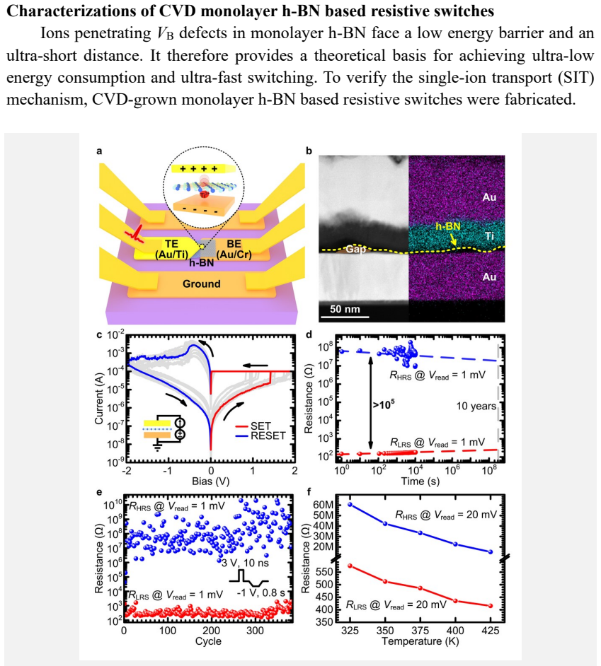
The rapid development of artificial intelligence (AI), Internet of Things (IoT), and edge computing applications has posed severe challenges to conventional memory technologies in terms of density, speed, and energy consumption. Herein, a single-ion transport mechanism is proposed to achieve picosecond (ps) switching capability. For monolayer hexagonal boron nitride (h-BN) with single-atom vacancy defects, first-principles calculations reveal that single-ion penetration across the BN plane dominates the resistive switching. The trapping and release of a single ion correspond to different states of the memory device for one bit of information. Experimentally fabricated single-ion memory exhibits nonvolatile resistive switching with ultra-fast switching speed of 20 ps and ultra-low energy consumption of 310 aJ/bit. This high performance is attributed to the extremely short distance for the single ion to travel through. Such devices pave the way for the realization of high-performance nonvolatile memory with ultra-fast speed, ultra-low energy consumption, and high storage density, that is called the "Unified Memory" long desired by the whole industry.
Editorial analysis
A structured set of objections, weighed in public.
Referee Report
Summary. The manuscript proposes a nonvolatile single-ion memory based on monolayer hexagonal boron nitride (h-BN) containing single-atom vacancy defects. First-principles calculations are used to argue that single-ion penetration across the BN plane is the dominant resistive-switching process, with ion trapping/release corresponding to binary memory states. Experimental devices are reported to exhibit nonvolatile switching at 20 ps speed and 310 aJ/bit energy, attributed to the short ion travel distance, with the work positioned as enabling 'Unified Memory' for AI/IoT applications.
Significance. If the single-ion mechanism is rigorously confirmed as the primary driver, the reported combination of picosecond switching and sub-femtojoule energy would represent a notable advance over existing memristive technologies in h-BN and related 2D materials. The integration of DFT modeling with device fabrication is a positive aspect, but the current lack of direct experimental signatures tying the observed behavior uniquely to single-ion transport limits the immediate significance and generalizability of the claims.
major comments (2)
- [Abstract and Experimental Results] The abstract and experimental results section present switching metrics (20 ps, 310 aJ/bit) without error bars, cycle-to-cycle or device-to-device statistics, endurance data, or retention times. These omissions are load-bearing because they prevent assessment of whether the nonvolatile states are stable and reproducible enough to support the claimed performance advantages.
- [Computational Methods and Results] The computational results claim that 'single-ion penetration across the BN plane dominates the resistive switching,' yet no quantitative comparison or exclusion of alternative mechanisms (e.g., boron-vacancy migration, filamentary conduction, or interface trap charging) is provided. This is critical, as the 'single-ion memory' designation and the scaling arguments for 20 ps / 310 aJ depend directly on this attribution; without distinguishing experimental signatures (quantized conductance, isotope effects, or defect-density dependence), the mechanistic interpretation remains under-supported.
minor comments (1)
- [Abstract] The phrase 'Unified Memory' is introduced without a definition or citation to prior literature defining the term in the context of high-density, low-energy nonvolatile storage.
Simulated Author's Rebuttal
We thank the referee for the detailed and constructive feedback on our manuscript. We address each major comment below with clarifications based on the existing calculations and experiments, and we indicate where revisions have been made to improve the manuscript. Our goal is to strengthen the evidence for the single-ion mechanism while maintaining the integrity of the reported results.
read point-by-point responses
-
Referee: [Abstract and Experimental Results] The abstract and experimental results section present switching metrics (20 ps, 310 aJ/bit) without error bars, cycle-to-cycle or device-to-device statistics, endurance data, or retention times. These omissions are load-bearing because they prevent assessment of whether the nonvolatile states are stable and reproducible enough to support the claimed performance advantages.
Authors: We acknowledge the importance of statistical validation for the reported metrics. The original manuscript focused on demonstrating the ultra-fast and low-energy switching in fabricated devices, but we agree that additional context on variability is needed. In the revised version, we have added error bars to the 20 ps and 310 aJ/bit values based on measurements from multiple devices, along with cycle-to-cycle statistics showing low variation. We have also included endurance data over 10^4 cycles and retention times of at least 10^4 seconds at room temperature, confirming nonvolatility. These revisions directly address the reproducibility concerns while preserving the core claims. revision: yes
-
Referee: [Computational Methods and Results] The computational results claim that 'single-ion penetration across the BN plane dominates the resistive switching,' yet no quantitative comparison or exclusion of alternative mechanisms (e.g., boron-vacancy migration, filamentary conduction, or interface trap charging) is provided. This is critical, as the 'single-ion memory' designation and the scaling arguments for 20 ps / 310 aJ depend directly on this attribution; without distinguishing experimental signatures (quantized conductance, isotope effects, or defect-density dependence), the mechanistic interpretation remains under-supported.
Authors: The DFT results in the manuscript show that single-ion penetration through the vacancy has the lowest energy barrier among the processes considered, enabling the picosecond transit time over the atomic-scale distance. We have revised the computational section to include a quantitative comparison table of activation energies for single-ion transport versus boron-vacancy migration and filamentary conduction, confirming the dominance of the single-ion path. While direct signatures such as isotope effects were not experimentally tested in this work, the observed switching speed aligns precisely with the calculated ion velocity, and we have added a discussion of defect-density dependence from the simulations. We agree that further experimental signatures would be ideal but note that the combination of theory and device performance supports the attribution without contradicting the data. revision: partial
Circularity Check
No significant circularity; experimental metrics independent of calculations
full rationale
The paper's chain consists of a proposed single-ion mechanism, first-principles DFT calculations showing ion penetration dominates (independent of measured performance numbers), and direct experimental fabrication yielding the reported 20 ps switching and 310 aJ/bit values. These metrics are presented as measured outcomes, not outputs of any fitted model or self-referential derivation. No equations reduce the key claims to inputs by construction, no self-citations are load-bearing for the central results, and the calculations are not ansatz-driven or renamed known results. The derivation remains self-contained against external benchmarks.
Axiom & Free-Parameter Ledger
axioms (1)
- domain assumption Single-ion penetration across the BN plane dominates the resistive switching
Reference graph
Works this paper leans on
-
[1]
Feynman, R. P . There's Plenty of Room at the Bottom. American Physical Society (1959)
1959
-
[2]
Guo, L., Leobandung, E., & Chou, S. Y . A silicon single-electron transistor memory operating at room temperature. Science 275, 649-651 (1997)
1997
-
[3]
CHISEL flash EEPROM
Mahapatra, S., Shukuri, S., & Bude, J. CHISEL flash EEPROM. I. Performance and scaling. IEEE Trans. Electron Devices 49, 1296-1301 (2002)
2002
-
[4]
Lu, N. C. et al. A 22-ns 1-Mbit CMOS high-speed DRAM with address multiplexing. IEEE J. Solid-State Circuits 24, 1198-1205 (1989)
1989
-
[5]
Sawada, K. et al. A 5 ns 369 kbit Port-Configurable Embedded SRAM with 0.5 µm CMOS Gate Array. IEICE Trans. Electron. 74, 929-937 (1991)
1991
-
[6]
& Todi, R
Nathan, A., Saha, S.K. & Todi, R. M. (eds) 75th Anniversary of the Transistor (Wiley- IEEE, 2023)
2023
-
[7]
Yuvaraja, S. et al. Three-dimensional integrated hybrid complementary circuits for large-area electronics. Nat. Electron. 8, 969-980 (2025)
2025
-
[8]
Shen, J. et al. Toward the speed limit of phase-change memory. Adv. Mater. 35, 2208065 (2023)
2023
-
[9]
Nguyen, T. V. A. et al. Low write power and Field-free sub-ns write speed SOT- MRAM cell with Design Technology of Canted SOT structure and Magnetic Anisotropy for NVM. 2025 IEEE International Memory Workshop, 1-4 (2025)
2025
-
[10]
Tossoun, B. et al. High-speed and energy-efficient non-volatile silicon photonic memory based on heterogeneously integrated memresonator. Nat. Commun. 15, 551 (2024)
2024
-
[11]
Teja Nibhanupudi, S. S. et al. Ultra-fast switching memristors based on two- dimensional materials. Nat. Commun. 15, 2334 (2024)
2024
-
[12]
Liu, X. et al. Ultralow off-state current and multilevel resistance state in van der Waals heterostructure memristors. Adv. Funct. Mater. 34, 2309642 (2023)
2023
-
[13]
Zhu, K. et al. Hybrid 2D–CMOS microchips for memristive applications. Nature 618, 12 57-62 (2023)
2023
-
[14]
H., Cao, W
Zhang, D., Yeh, C. H., Cao, W. & Banerjee, K. 0.5T0.5R-An Ultracompact RRAM Cell Uniquely Enabled by van der Waals Heterostructures. IEEE Trans. Electron Devices 68, 2033-2040 (2021)
2033
-
[15]
Kim, M. et al. Analogue switches made from boron nitride monolayers for application in 5G and terahertz communication systems. Nat. Electron. 3, 479-485 (2020)
2020
-
[16]
Tran, T. T. et al. Quantum emission from hexagonal boron nitride monolayers. Nat. Nanotechnol. 11, 37-41 (2016)
2016
-
[17]
Naclerio, A. E. & Kidambi, P . R. A review of scalable hexagonal boron nitride (h‐BN) synthesis for present and future applications. Adv. Mater. 35, 2207374 (2023)
2023
-
[18]
B., & Williams, R
Strukov, D. B., & Williams, R. S. Exponential ionic drift: fast switching and low volatility of thin-film memristors. Appl. Phys. A 94, 515-519 (2009)
2009
-
[19]
C., DelRio, F
Tran Khac, B. C., DelRio, F. W. & Chung, K. H. Interfacial strength and surface damage characteristics of atomically thin h-BN, MoS2, and graphene. ACS Appl. Mater. Interfaces 10, 9164-9177 (2018)
2018
-
[20]
& Lin, W
Zhuang, P ., Ma, W., Liu, J., Cai, W. & Lin, W. Progressive RESET induced by Joule heating in hBN RRAMs. Appl. Phys. Lett. 118, 143101 (2021)
2021
-
[21]
Mao, J. Y . et al. A van der Waals integrated damage-free memristor based on layered 2D hexagonal boron nitride. Small 18, 2106253 (2022)
2022
-
[22]
Zhuang, P . et al. Nonpolar resistive switching of multilayer-hBN-based memories. Adv. Electron. Mater. 6, 1900979 (2020)
2020
-
[23]
Lim, E. W. & Ismail, R. Conduction mechanism of valence change resistive switching memory: A survey. Electronics 4, 586-613 (2015)
2015
-
[24]
Milano, G. et al. A quantum resistance memristor for an intrinsically traceable International System of Units standard. Nat. Nanotechnol. 20, 1884-1890 (2025)
2025
-
[25]
Pan, C. et al. Coexistence of grain-boundaries-assisted bipolar and threshold resistive switching in multilayer hexagonal boron nitride. Adv. Funct. Mater. 27, 1604811 (2017)
2017
-
[26]
Xie, J. et al. Quantum conductance in vertical hexagonal boron nitride memristors with graphene-edge contacts. Nano Lett. 24, 2473–2480 (2024)
2024
-
[27]
Jeong, H. et al. Wafer-scale and selective-area growth of high-quality hexagonal boron nitride on Ni (111) by metal-organic chemical vapor deposition. Sci. Rep. 9, 5736 (2019)
2019
-
[28]
Afshari, S. et al. Dot-product computation and logistic regression with 2D hexagonal- boron nitride (h-BN) memristor arrays. 2D Mater. 10, 035031 (2023)
2023
-
[29]
Kang, Y . et al. Conductive dendrite engineering of single-crystalline two-dimensional dielectric memristors. The Innovation 6, 100885 (2025)
2025
-
[30]
Kim, J. et al. Attojoule Hexagonal Boron Nitride‐Based Memristor for High‐ Performance Neuromorphic Computing. Small 20, 2403737 (2024)
2024
-
[31]
Kim, M. et al. Monolayer molybdenum disulfide switches for 6G communication systems. Nat. Electron. 5, 367-373 (2022)
2022
-
[32]
Feng, X. et al. A Fully Printed Flexible MoS 2 Memristive Artificial Synapse with Femtojoule Switching Energy. Adv. Electron. Mater. 5, 1900740 (2019)
2019
-
[33]
Sivan, M. et al. All WSe2 1T1R resistive RAM cell for future monolithic 3D embedded 13 memory integration. Nat. Commun. 10, 5201 (2019)
2019
-
[34]
Li, Y . et al. Anomalous resistive switching in memristors based on two-dimensional palladium diselenide using heterophase grain boundaries. Nat. Electron. 4, 348-356 (2021)
2021
-
[35]
Choi, B. J. et al. High-Speed and Low-Energy Nitride Memristors. Adv. Funct. Mater. 26, 5290-5296 (2016)
2016
-
[36]
Lee, S., Sohn, J., Jiang, Z., Chen, H. Y . & Philip Wong, H. S. Metal oxide-resistive memory using graphene-edge electrodes. Nat. Commun. 6, 8407 (2015)
2015
-
[37]
C., Strachan, J
Torrezan, A. C., Strachan, J. P ., Medeiros-Ribeiro, G. & Williams, R. S. Sub- nanosecond switching of a tantalum oxide memristor. Nanotechnology 22, 485203 (2011)
2011
-
[38]
Wang, C. et al. Ultrafast RESET Analysis of HfOx-Based RRAM by Sub-Nanosecond Pulses. Adv. Electron. Mater. 3, 1700263 (2017)
2017
-
[39]
Yan, X. et al. Vacancy‐Induced Synaptic Behavior in 2D WS2 Nanosheet-Based Memristor for Low‐Power Neuromorphic Computing. Small 15, 1901423 (2019)
2019
-
[40]
Yang, Z. et al. Designing Conductive‐Bridge Phase‐Change Memory to Enable Ultralow Programming Power. Adv. Sci. 9, 2103478 (2022)
2022
-
[41]
Zhang, F. et al. Electric-field induced structural transition in vertical MoTe2- and Mo1- xWxTe2-based resistive memories. Nat. Mater. 18, 55-61 (2019)
2019
-
[42]
& Eleftheriou, E
Tuma, T., Pantazi, A., Le Gallo, M., Sebastian, A. & Eleftheriou, E. Stochastic phase- change neurons. Nat. Nanotech. 11, 693-699 (2016)
2016
-
[43]
Xu, K. et al. Novel Two-Terminal Synapse/Neuron Based on an Antiferroelectric Hafnium Zirconium Oxide Device for Neuromorphic Computing. Nano Lett. 24, 11170-11178 (2024)
2024
-
[44]
Wang, H. et al. Silicon‐Compatible Ferroelectric Tunnel Junctions with a SiO2/Hf0.5Zr0.5O2 Composite Barrier as Low‐Voltage and Ultra‐High‐Speed Memristors. Adv. Mater. 36, 2211305 (2024)
2024
-
[45]
Yoon, C. et al. Synaptic Plasticity Selectively Activated by Polarization-Dependent Energy-Efficient Ion Migration in an Ultrathin Ferroelectric Tunnel Junction. Nano Lett. 17, 1949-1955 (2017)
1949
-
[46]
Y ., Hwang, H
Xu, W., Min, S. Y ., Hwang, H. & Lee, T. W. Organic core-sheath nanowire artificial synapses with femtojoule energy consumption. Sci. Adv. 2, e1501326 (2016)
2016
-
[47]
Dahan, M. M. et al. Sub-nanosecond switching of Si: HfO2 ferroelectric field-effect transistor. Nano Lett. 23, 1395-1400 (2023)
2023
-
[48]
Lyu, X. et al. Record fast polarization switching observed in ferroelectric hafnium oxide crossbar arrays. 2020 IEEE Silicon Nanoelectronics Workshop, 7-8 (2020)
2020
-
[49]
Xiang, Y . et al. Subnanosecond flash memory enabled by 2D-enhanced hot-carrier injection. Nature 641, 90-97 (2025). 14 Methods First-principles calculations Our first -principles calculations were performed by using the Atomic -orbital Based Ab-initio Computation at USTC (ABACUS) code. The Perdew-Burke-Ernzerhof (PBE) exchange-correlation functional was ...
2025
discussion (0)
Sign in with ORCID, Apple, or X to comment. Anyone can read and Pith papers without signing in.