Recognition: 2 theorem links
· Lean TheoremSurface nanostructuring of NbTi superconducting thin-film resonators for enhanced cryogenic thermometry
Pith reviewed 2026-05-08 19:07 UTC · model grok-4.3
The pith
Nanostructuring NbTi resonators with nanogaps lowers critical temperature by 1.5 K and boosts temperature sensitivity tenfold.
A machine-rendered reading of the paper's core claim, the machinery that carries it, and where it could break.
Core claim
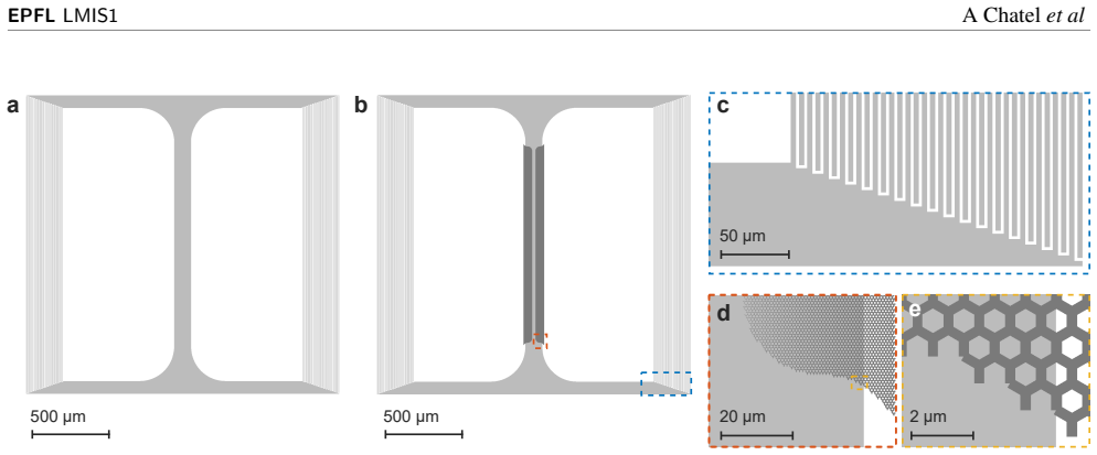
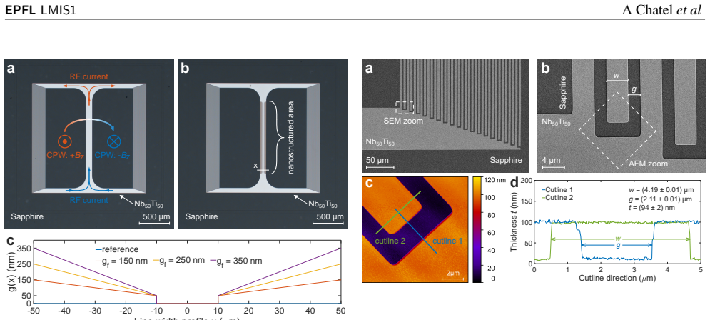
Patterning different arrays of nanogaps on the inductive line of 1.3 GHz planar resonators fabricated from Nb50Ti50 thin films tunes the superconductor's critical transition temperature downward by up to 1.5 K. This adjustment increases the curvature of the resonance frequency versus temperature curve, directly raising the temperature sensitivity by a factor of ten relative to a non-nanostructured reference. The largest effect occurs with nanogap widths around 350 nm, reaching dfres/dT = 62 MHz/K at 4.2 K while microwave losses stay low enough for practical thermometry.
What carries the argument
Arrays of nanogaps etched into the NbTi inductive line that function as weak links to lower the critical temperature and steepen the frequency-temperature response.
Load-bearing premise
The nanogaps lower the critical temperature enough to increase the curvature of the frequency-temperature curve while the added microwave losses remain small enough for usable thermometry.
What would settle it
Measure resonance frequency versus temperature from 2 K to 6 K on both a reference resonator without nanogaps and one with 350 nm nanogaps; the structured device must show a peak dfres/dT near 62 MHz/K at 4.2 K while the reference stays near 6 MHz/K.
Figures


read the original abstract
The rising complexity of cutting-edge cryogenic systems is currently imposing challenging technical constraints to the monitoring of ultra-cold temperatures through standard commercially available sensors. Among different alternative technologies, superconducting microwave resonators have been recently investigated as ideal candidates for performing on-chip cryogenic thermometry, in reason of their intrinsically low power dissipation, typically large temperature sensitivities and excellent sub-mK resolution below 10 K. In such a framework, through this study we aim at demonstrating the possibility to enhance the temperature performance of superconducting microwave resonators by means of surface nanostructuring. More specifically, different arrays of nanogaps are strategically patterned on the inductive line of a 1.3 GHz planar resonator, by partially etching a Nb50Ti50 thin film, in order to tune the critical transition of the material and, therefore, increase the curvature of the fres(T) response. Although the presence of such weak-links introduces larger microwave losses, a 1.5 K decrease of TC is recorded, which directly translates into an enhancement of the temperature sensitivity by a factor 10, with respect to a reference non-nanostructured sensor. In particular, a maximum value of dfres/dT = 62 MHz/K, at 4.2 K, is achieved for the device showing the largest nanogap width of about 350 nm, demonstrating that the surface nanostructuring of superconducting thin-films can be effectively engineered to enhance the temperature response of microwave resonators for high-performance cryogenic thermometry. We believe that similar approaches might be investigated and, eventually, adopted for the near-future development of the next generation of low-temperature sensors.
Editorial analysis
A structured set of objections, weighed in public.
Referee Report
Summary. The paper reports an experimental demonstration of surface nanostructuring on NbTi thin-film microwave resonators to enhance cryogenic thermometry performance. Arrays of nanogaps are etched into the inductive line of 1.3 GHz planar resonators to introduce weak links that reduce the critical temperature TC by 1.5 K relative to a reference device. This shift is claimed to increase the curvature of the resonance frequency versus temperature curve, yielding up to a 10x improvement in temperature sensitivity with a peak value of dfres/dT = 62 MHz/K at 4.2 K for the largest (~350 nm) nanogap width. The work notes increased microwave losses but argues the approach remains viable for low-power on-chip sensors.
Significance. If the reported TC reduction is shown to be a controllable geometric effect of the nanogaps (rather than film damage or measurement artifact) and the sensitivity gain is reproducible with acceptable resonator Q, the result would provide a practical route to higher-sensitivity superconducting thermometers for complex cryogenic systems. The experimental focus on geometry-tuned weak links in resonators is a concrete contribution, though the absence of error bars, raw curves, and independent TC verification limits immediate impact.
major comments (3)
- Abstract and results: The central claim of a 1.5 K TC decrease (and the resulting 10x sensitivity boost) is presented without any description of how TC is extracted from the resonator data, without error bars on the 1.5 K or 62 MHz/K figures, and without a comparison of microwave-derived TC to DC transport measurements on the same films. This extraction method is load-bearing for attributing the dfres/dT enhancement specifically to nanogap-induced weak links.
- Results/discussion: No quantitative data are given on resonator quality factors or internal losses before versus after nanostructuring. The abstract acknowledges larger microwave losses, but without numbers it is impossible to assess whether the devices remain practical for thermometry (i.e., whether the sensitivity gain outweighs any degradation in signal-to-noise or power handling).
- Methods/results: The manuscript should include raw frequency-temperature curves for all devices (including the reference) and a clear statement of the temperature range and fitting procedure used to obtain dfres/dT. Without these, the factor-of-10 enhancement cannot be independently verified from the reported data.
minor comments (1)
- Abstract: The phrase 'partially etching a Nb50Ti50 thin film' would benefit from a brief clarification of etch depth relative to film thickness to confirm the nanogaps act as weak links rather than complete cuts.
Simulated Author's Rebuttal
We thank the referee for their constructive comments on our manuscript. We address each major comment below and will revise the manuscript accordingly to improve clarity and completeness.
read point-by-point responses
-
Referee: Abstract and results: The central claim of a 1.5 K TC decrease (and the resulting 10x sensitivity boost) is presented without any description of how TC is extracted from the resonator data, without error bars on the 1.5 K or 62 MHz/K figures, and without a comparison of microwave-derived TC to DC transport measurements on the same films. This extraction method is load-bearing for attributing the dfres/dT enhancement specifically to nanogap-induced weak links.
Authors: We agree that the TC extraction method requires explicit description. In the revised manuscript we will add a detailed explanation in the Methods section of how TC is determined from the resonance frequency data, along with error bars on the reported 1.5 K shift and 62 MHz/K sensitivity values. DC transport measurements on the same films were not performed, as the study focused on microwave resonator properties; we will add a brief discussion of this limitation while maintaining that the geometric control via nanogaps and comparison to the reference device supports the weak-link interpretation. revision: partial
-
Referee: Results/discussion: No quantitative data are given on resonator quality factors or internal losses before versus after nanostructuring. The abstract acknowledges larger microwave losses, but without numbers it is impossible to assess whether the devices remain practical for thermometry (i.e., whether the sensitivity gain outweighs any degradation in signal-to-noise or power handling).
Authors: We acknowledge the absence of quantitative Q and loss data. The revised manuscript will include measured quality factors and internal loss values for both the nanostructured devices and the reference resonator at relevant temperatures and low drive powers. These data will show that the increase in losses remains compatible with practical low-power thermometry use, with the sensitivity gain providing a net benefit. revision: yes
-
Referee: Methods/results: The manuscript should include raw frequency-temperature curves for all devices (including the reference) and a clear statement of the temperature range and fitting procedure used to obtain dfres/dT. Without these, the factor-of-10 enhancement cannot be independently verified from the reported data.
Authors: We will include the raw fres(T) curves for all devices (reference and nanostructured) in the revised manuscript or supplementary material. We will also add an explicit statement of the temperature range explored and the numerical procedure used to extract dfres/dT, enabling independent verification of the reported sensitivity improvement. revision: yes
Circularity Check
No circularity: purely experimental measurements with no derivations or self-referential claims
full rationale
The paper reports fabrication of NbTi resonators with nanogap arrays, direct measurements of resonance frequency vs temperature, and observed TC shifts and dfres/dT values. No equations, derivations, fitted parameters renamed as predictions, or load-bearing self-citations appear in the provided text or abstract. The central claims rest on experimental data comparison between nanostructured and reference devices, which is self-contained and externally falsifiable via replication. This matches the default expectation for experimental reports with no mathematical chain to inspect.
Axiom & Free-Parameter Ledger
Reference graph
Works this paper leans on
-
[1]
Mukhatov, A. and Le, T.-A. and Pham, T. T. and Do, T. D. A comprehensive review on magnetic imaging techniques for biomedical applications. Nano Sel. https://doi.org/10.1002/nano.202200219. 2023
-
[2]
Manso Jimeno, M. and Vaughan, J. T. and Geethanath, S. Superconducting magnet designs and MRI accessibility: A review. NMR Biomed. https://doi.org/10.1002/nbm.4921. 2023
-
[3]
O’Connor, E. G. P. and Shearer, A. and O’Brien, K. Energy-sensitive detectors for astronomy: Past, present and future. New Astron. Rev. https://doi.org/10.1016/j.newar.2020.101526. 2019
-
[4]
Awschalom, D. D. and Bernien, H. and Hanson, R. and Oliver, W. D. and Vučković, J. Challenges and opportunities for quantum information hardware. Science https://doi.org/10.1126/science.adz8659. 2025
-
[5]
Bottura, L. and Prestemon, S. and Rossi, L. and Zlobin, A. V. Superconducting magnets and technologies for future colliders. Front. Phys. https://doi.org/10.3389/fphy.2022.935196. 2022
-
[6]
Onnes, H. K. On the cryogenic laboratory at Leiden and on the production of very low temperatures. Commun. Phys. Lab. Univ. Leiden. 1894
-
[7]
Kurti, N. Low temperature terminology. Cryogenics https://doi.org/10.1016/0011-2275(70)90099-8. 1970
-
[8]
Historical summary of cryogenic activity prior to 1950
Radebaugh, R. Historical summary of cryogenic activity prior to 1950. Cryogenic Engineering: Fifty Years of Progress. 2007
1950
-
[9]
Case studies in superconducting magnets: Design and operational issues
Iwasa, Y. Case studies in superconducting magnets: Design and operational issues. 2009
2009
-
[10]
Huang, P. and Zheng, H. Effect of bath temperature on the quantum decoherence. Chem. Phys. Lett. https://doi.org/10.1016/j.cplett.2010.10.009. 2010
-
[11]
Simbierowicz, S. and Borrelli, M. and Monarkha, V. and Nuutinen, V. and Lake, R. E. Inherent thermal-noise problem in addressing qubits. PRX Quantum https://doi.org/10.1103/PRXQuantum.5.030302. 2024
-
[12]
Gansen, E. J. and Rowe, M. A. and Harrington, S. D. and Nehls, J. M. and Etzel, S. M. and Nam, S. W. and Mirin, R. P. Temperature dependence of the single-photon sensitivity of a quantum dot, optically gated, field-effect transistor. J. Appl. Phys. https://doi.org/10.1063/1.4820474. 2013
-
[13]
Bahgat Shehata, A. and Ruggeri, A. and Stellari, F. and Weger, A. J. and Song, P. and Sunter, K. and Najafi, F. and Berggren, K. K. and Anant, V. Effect of temperature on superconducting nanowire single-photon detector noise. Optical Sensing, Imaging, and Photon Counting: Nanostructured Devices and Applications https://doi.org/10.1117/12.2188234. 2015
-
[14]
Wandui, A. and Bock, J. J. and Frez, C. and Hollister, M. and Minutolo, L. and Nguyen, H. and Steinbach, B. and Turner, A. and Zmuidzinas, J. and O’Brient, R. Thermal kinetic inductance detectors for millimeter-wave detection. J. Appl. Phys. https://doi.org/10.1063/5.0002413. 2020
-
[15]
Todesco, E. and Annarella, M. and Ambrosio, G. and Apollinari, G. and Ballarino, A. and Bajas, H. and Bajko, M. and Bordini, B. and Bossert, R. and Bottura, L. and Cavanna, E. and Cheng, D. and Chlachidze, G. and De Rijk, G. and DiMarco, J. and Ferracin, P. and Fleiter, J. and Guinchard, M. and Hafalia, A. and Holik, E. and Izquierdo Bermudez, S. and Lack...
-
[16]
Turqueti, M. and Prestemon, S. and Albright, R. Deep cryogenic low power 24 bits analog to digital converter with active reverse cryostat. Phys. Procedia https://doi.org/10.1016/j.phpro.2015.06.183. 2015
-
[17]
Schooley, J. F. NBS/NIST gas thermometry from 0 to 660 °C. J. Res. Natl. Inst. Stand. Technol. https://doi.org/10.6028/jres.095.028. 1990
-
[18]
Qu, J. F. and Benz, S. P. and Rogalla, H. and Tew, W. L. and White, D. R. and Zhou, K. L. Johnson noise thermometry. Meas. Sci. Technol. https://doi.org/10.1088/1361-6501/ab3526. 2019
-
[19]
Pekola, J. P. and Hirvi, K. P. and Kauppinen, J. P. and Paalanen, M. A. Thermometry by arrays of tunnel junctions. Phys. Rev. Lett. https://doi.org/10.1103/PhysRevLett.73.2903. 1994
-
[20]
Rusby, R. L. and Kempson, M. Cryogenic temperature measurement. Rev. Gén. Therm. https://doi.org/10.1016/S0035-3159(99)80076-2. 1996
-
[21]
Brandt, B. L. and Liu, D. W. and Rubin, L. G. Low temperature thermometry in high magnetic fields. VII. Cernox™ sensors to 32 T. Rev. Sci. Instrum. https://doi.org/10.1063/1.1149549. 1999
-
[22]
Sullivan, N. S. and Edwards, C. M. Carbon resistance thermometers and variable-range hopping. Cryogenics https://doi.org/10.1016/S0011-2275(86)80001-7. 1986
-
[23]
De Cosmo , V. and Gush, H. and Halpern, M. and Leung, A. Carbon composition resistors for cryogenic thermometry. Rev. Sci. Instrum. https://doi.org/10.1063/1.1139251. 1987
-
[24]
Courts, S. S. and Krause, J. K. A commercial ruthenium oxide thermometer for use to 20 millikelvin , journal = ". 2008
2008
-
[25]
Mansoor, M. and Haneef, I. and Akhtar, S. and De Luca , A. and Udrea, F. Silicon diode temperature sensors — A review of applications. Sens. Actuators A: Phys. https://doi.org/10.1016/j.sna.2015.04.022. 2015
-
[26]
Scurti, F. and Ishmael, S. and Flanagan, G. and Schwartz, J. Quench detection for high temperature superconductor magnets: a novel technique based on Rayleigh-backscattering interrogated optical fibers. Supercond. Sci. Technol. https://doi.org/10.1088/0953-2048/29/3/03LT01. 2016
-
[27]
Scurti, F. and Schwartz, J. Optical fiber distributed sensing for high temperature superconductor magnets. 25th International Conference on Optical Fiber Sensors https://doi.org/10.1117/12.2265947. 2017
-
[28]
Yang, Y. and Soto, M. A. and Tévenaz, L. Absolute thermometry based on Brillouin scattering in gases. Light Sci. Appl. https://doi.org/10.1038/s41377-025-02168-3. 2025
-
[29]
Agatsuma, K. and Uchiyama, F. and Ohara, T. and Tukamoto, K. and Tateishi, H. and Fuchino, S. and Nobue, Y. and Ishigami, S. and Sato, M. and Sugimoto, H. Wireless cryogenic quartz thermometer with high resolution from 400 K to 4.2 K. https://doi.org/10.1007/978-1-4613-0639-9_185 Advances in Cryogenic Engineering: Part A & B. 1990
-
[30]
Agatsuma, K. and Uchiyama, F. and Ishigami, S. and Satoh, M. High resolution cryogenic quartz thermometer and application towireless measurement. Cryogenics https://doi.org/10.1016/S0011-2275(05)80092-X. 1994
-
[31]
Goshlya, R. Y. Quartz sensor for measuring cryogenic temperatures. AIP Conf. Proc. https://doi.org/10.1063/1.5122162. 2019
-
[32]
Andrews, D. H. and Brucksch, W. F., Jr. and Ziegler, W. T. and Blanchard, E. R. Attenuated superconductors I. for Measuring infra‐red radiation. Rev. Sci. Instrum. https://doi.org/10.1063/1.1770037. 1942
-
[33]
Irwin, K. D. An application of electrothermal feedback for high resolution cryogenic particle detection. Appl. Phys. Lett. https://doi.org/10.1063/1.113674. 1995
-
[34]
Nature431, 162–167 (2004) https://doi.org/10.1038/nature02851
Wallraff, A. and Schuster, D. I. and Blais, A. and Frunzio, L. and Huang, R.- S. and Majer, J. and Kumar, S. and Girvin, S. M. and Schoelkopf, R. J. Strong coupling of a single photon to a superconducting qubit using circuit quantum electrodynamics. Nature https://doi.org/10.1038/nature02851. 2004
-
[35]
Frunzio, L. and Wallraff, A. and Schuster, D. and Majer, J. and Schoelkopf, R. Fabrication and characterization of superconducting circuit QED devices for quantum computation. IEEE Trans. Appl. Supercond. https://doi.org/10.1109/TASC.2005.850084. 2005
-
[36]
Journal of Applied Physics104, 113904 (2008) https://doi.org/10.1063/1.3010859
Göppl, M. and Fragner, A. and Baur, M. and Bianchetti, R. and Filipp, S. and Fink, J. M. and Leek, P. J. and Puebla, G. and Steffen, L. and Wallraff, A. , title = ". J. Appl. Phys. https://doi.org/10.1063/1.3010859. 2008
-
[37]
Scarlino, P. and van Woerkom, D. J. and Stockklauser, A. and Koski, J. V. and Collodo, M. C. and Gasparinetti, S. and Reichl, C. and Wegscheider, W. and Ihn, T. and Ensslin, K. and Wallraff, A. , title = ". Phys. Rev. Lett. https://doi.org/10.1103/PhysRevLett.122.206802. 2019
-
[38]
Superconducting qubits: Current state of play,
Kjaergaard, M. and Schwartz, M. E. and Braumüller, J. and Krantz, P. and Wang, J. I.-J. and Gustavsson, S. and Oliver, W. D. Superconducting qubits: current state of play. Annu. Rev. Condens. Matter Phys. https://doi.org/10.1146/annurev-conmatphys-031119-050605. 2020
-
[39]
Koch, J. and Yu, T. M. and Gambetta, J. and Houck, A. A. and Schuster, D. I. and Majer, J. and Blais, A. and Devoret, M. H. and Girvin, S. M. and Schoelkopf, R. J. Charge-insensitive qubit design derived from the Cooper pair box. Phys. Rev. A https://doi.org/10.1103/PhysRevA.76.042319. 2007
-
[40]
Schreier, J. A. and Houck, A. A. and Koch, Jens and Schuster, D. I. and Johnson, B. R. and Chow, J. M. and Gambetta, J. M. and Majer, J. and Frunzio, L. and Devoret, M. H. and Girvin, S. M. and Schoelkopf, R. J. Suppressing charge noise decoherence in superconducting charge qubits. Phys. Rev. B https://doi.org/10.1103/PhysRevB.77.180502. 2008
-
[41]
Barends et al., Nature 508, 500 (2014) https://doi.org/10.1038/nature13171
Barends, R. and Kelly, J. and Megrant, A. and Veitia, A. and Sank, D. and Jeffrey, E. and White, T. C. and Mutus, J. and Fowler, A. G. and Campbell, B. and Chen, Y. and Chen, Z. and Chiaro, B. and Dunsworth, A. and Neill, C. and O'Malley, P. and Roushan, P. and Vainsencher, A. and Wenner, J. and Korotkov, A. N. and Cleland, A. N. and Martinis, J. M. Super...
-
[42]
Audley, M. D. and Kelley, R. L. and Rawley, G. L. A prototype kinetic inductance thermometer for X-ray calorimetry. J. Low. Temp. Phys. https://doi.org/10.1007/BF00693427. 1993
-
[43]
Day ,P. K. and LeDuc, H. G. and Mazin, B. A. and Vayonakis, A. and Zmuidzinas, J. A broadband superconducting detector suitable for use in large arrays. Nature https://doi.org/10.1038/nature02037. 2003
-
[44]
Maloney, P. R. and Czakon, N. G. and Day, P. K. and Downes, T. P. and Downes, R. and Gao, J. and Glenn, J. and Golwala, S. R. and Hollister, M. I. and LeDuc, H. G. and Mazin, B. A. and McHugh, S. G. and Noroozian, O. and Nguyen, H. T. and Sayers, J. and Schlaerth, J. A. and S., Seth and Vaillancourt, J. E. and Vayonakis, A. and Wilson, P. and Zmuidzinas, ...
-
[45]
Leduc, H. G. and Bumble, B. and Day, P. K. and Eom, B. H. and Gao, J. and Golwala, S. and Mazin, B. A. and McHugh, S. and Merrill, A. and Moore, D. C. and Noroozian, O. and Turner, A. D. and Zmuidzinas, J. Titanium nitride films for ultrasensitive microresonator detectors. Appl. Phys. Lett. https://doi.org/10.1063/1.3480420. 2010
-
[46]
Austermann, J. E. and Beall, J. A. and Bryan, S. A. and Dober, B. and Gao, J. and Hilton, G. and Hubmayr, J. and Mauskopf, P. and McKenney, C. M. and Simon, S. M. and Ullom, J. N. and Vissers, M. R. and Wilson, G. W. Millimeter-wave polarimeters using kinetic inductance detectors for TolTEC and beyond. J. Low. Temp. Phys. https://doi.org/10.1007/s10909-01...
-
[47]
Dibert, K. and Barry, P. and Pan, Z. and Anderson, A. and Benson, B. and Chang, C. and Karkare, K. and Li, J. and Natoli, T. and Rouble, M. and Shirokoff, E. and Stark, A. and the South Pole Telescope Collaboration. Development of MKIDs for measurement of the cosmic microwave background with the South Pole Telescope. J. Low. Temp. Phys. https://doi.org/10...
-
[48]
Vissers, M. R. and Erickson, R. P. and Ku, H.-S. and Vale, Leila and Wu, Xian and Hilton, G. C. and Pappas, D. P. Low-noise kinetic inductance traveling-wave amplifier using three-wave mixing. Appl. Phys. Lett. https://doi.org/10.1063/1.4937922. 2016
-
[49]
Superconducting parametric amplifiers: the state of the art in Josephson parametric amplifiers
Aumentado, J. Superconducting parametric amplifiers: the state of the art in Josephson parametric amplifiers. IEEE Microw. Mag. https://doi.org/10.1109/MMM.2020.2993476. 2020
-
[50]
Frasca, S. and Roy, C. and Beaulieu, G. and Scarlino, P. Three-wave-mixing quantum-limited kinetic inductance parametric amplifier operating at 6 T near 1 K. Phys. Rev. Appl. https://doi.org/10.1103/PhysRevApplied.21.024011. 2024
-
[51]
Bienfait, A. and Pla, J. J. and Kubo, Y. and Stern, M. and Zhou, X. and Lo, C. C. and Weis, C. D. and Schenkel, T. and Thewalt, M. L. W. and Vion, D. and Esteve, D. and Julsgaard, B. and Mølmer, K. and Morton, J. J. L. and Bertet, P. Reaching the quantum limit of sensitivity in electron spin resonance. Nat. Nanotechnol. https://doi.org/10.1038/nnano.2015....
-
[52]
Artzi, Y. and Yishay, Y. and Fanciulli, M. and Jbara, M. and Blank, A. Superconducting micro-resonators for electron spin resonance - the good, the bad, and the future. J. Mag. Res. https://doi.org/10.1016/j.jmr.2021.107102. 2021
-
[53]
Ranjan, V. and Probst, S. and Albanese, B. and Schenkel, T. and Vion, D. and Esteve, D. and Morton, J. J. L. and Bertet, P. Electron spin resonance spectroscopy with femtoliter detection volume. Appl. Phys. Lett. https://doi.org/10.1063/5.0004322. 2020
-
[54]
Akhmetzyanov, D. and Borneman, T. W. and Taminiau, I. and Sadeghi, S. and Mohebbi, H. R. and Cory, D. G. Electron spin resonance spectroscopy using a Nb superconducting resonator. Appl. Phys. Lett. https://doi.org/10.1063/5.0172139. 2023
-
[55]
Courts, S. S. and Swinehart, P. R. Review of Cernox™ (Zirconium Oxy‐Nitride) Thin‐Film Resistance Temperature Sensors. AIP Conf. Proc. https://doi.org/10.1063/1.1627157. 2003
-
[56]
A standardized Cernox™ cryogenic temperature sensor for aerospace applications
Courts, S.S. A standardized Cernox™ cryogenic temperature sensor for aerospace applications. Cryogenics https://doi.org/10.1016/j.cryogenics.2014.03.009. 2014
-
[57]
Myers, S. A. and Li, H. and Csáthy, G. A. A ruthenium oxide thermometer for dilution refrigerators operating down to 5 mK. Cryogenics https://doi.org/10.1016/j.cryogenics.2021.103367. 2021
-
[58]
Holmes, D. S. and Courts, S. S. Resolution and accuracy of cryogenic temperature measurements. Temperature: Its Measurement and Control in Science and Industry https://citeseerx.ist.psu.edu/document?repid=rep1&type=pdf&doi=8c055433b68ba63a23823d900065bbe38e9c7d63. 1992
1992
-
[59]
Yeager, C. J. and Courts, S. S. A review of cryogenic thermometry and common temperature sensors. IEEE Sens. J. https://doi.org/10.1109/7361.983476. 2001
-
[60]
Experimental Techniques for Low-Temperature Measurements: Cryostat Design, Material Properties and Superconductor Critical-Current Testing
Ekin, J. Experimental Techniques for Low-Temperature Measurements: Cryostat Design, Material Properties and Superconductor Critical-Current Testing. 2006
2006
-
[61]
Feshchenko, A. V. and Casparis, L. and Khaymovich, I. M. and Maradan, D. and Saira, O.-P. and Palma, M. and Meschke, M. and Pekola, J. P. and Zumbühl, D. M. Tunnel-junction thermometry down to millikelvin temperatures. Phys. Rev. Appl. https://doi.org/10.1103/PhysRevApplied.4.034001. 2015
-
[62]
Noah, G. M. and Swift, T. H. and de Kruijf, M. and Gomez-Saiz, A. and Morton, J. J. L. and Gonzalez-Zalba, M. F. CMOS on-chip thermometry at deep cryogenic temperatures. Appl. Phys. Rev. https://doi.org/10.1063/5.0190040. 2024
-
[63]
Olivadese, S. B. and Bogorin, D. F. and Bronn, N. T. and Hart, S. and Gumann, P. On-chip thermometer for superconducting quantum computing devices. 2019
2019
-
[64]
Wheeler, J. and Vissers, M. R. and Malnou, M. and Hubmayr, J. and Ullom, J. N. and Gao, J. Sub-kelvin thermometer for on-chip measurements of microwave devices utilizing two-level systems in superconducting microresonators. Appl. Phys. Lett. https://doi.org/10.1063/5.0029351. 2020
-
[65]
Yu, H. and Jing, L. and Hua, T. and Xu, W. Temperature and power characteristics of quarter-wavelength superconducting coplanar waveguide resonator. SN Appl. Sci. https://doi.org/10.1007/s42452-022-04956-7. 2022
-
[66]
Nulens, L. and Lejeune, N. and Caeyers, J. and Marinković, S. and Cools, I. and Dausy, H. and Basov, S. and Raes, B. and Van Bael, M. J. and Geresdi, A. and Silhanek, A. V. and Van de Vondel, J. Catastrophic magnetic flux avalanches in NbTiN superconducting resonators. Commun. Phys. https://doi.org/10.1038/s42005-023-01386-8. 2023
-
[67]
Gorter, C. J. and Casimir, H. On supraconductivity I. Physica https://doi.org/10.1016/S0031-8914(34)90037-9. 1934
-
[68]
Hossain, M. S. and Yoshida, K. and Kudo, K. and Keiji, K. and Kaoru, Y. Enlargement of kinetic inductance of NbN superconducting thin films for device applications. Jpn. J. Appl. Phys. https://doi.org/10.1143/JJAP.31.1033. 1992
-
[69]
Watanabe, K. and Yoshida, K. and Kohjiro, T. A. Kinetic inductance of superconducting coplanar waveguides. Jpn. J. Appl. Phys. https://doi.org/10.1143/JJAP.33.5708. 1994
-
[70]
Yoshida, K. and Watanabe, K. and Kisu, T. and Enpuku, K. Evaluation of magnetic penetration depth and surface resistance of superconducting thin films using coplanar waveguides. IEEE Trans. Appl. Supercond. https://doi.org/10.1109/77.402973. 1995
-
[71]
Hein, M. A. Microwave properties of superconductors. Microwave superconductivity https://doi.org/10.1007/978-94-010-0450-3_2. 2001
-
[72]
Introduction to Superconductivity
Tinkham, M. Introduction to Superconductivity. 2004
2004
-
[73]
Annunziata, A. J. and Santavicca, D. F. and Frunzio, L. and Catelani, G. and Rooks, M. J. and Frydman, A. and Prober, D. E. Tunable superconducting nanoinductors. Nanotechnol. https://doi.org/10.1088/0957-4484/21/44/445202. 2010
-
[74]
Bychkov, Y. F. and Herzog, R. and Khukhareva, I. S. Thermal conductivity and electrical resistivity of NbTi alloys at low temperatures. Cryogenics https://doi.org/10.1016/0011-2275(81)90219-8. 1981
-
[75]
A practical fit for the critical surface of NbTi
Bottura, L. A practical fit for the critical surface of NbTi. IEEE Trans. Appl. Supercond. https://doi.org/10.1109/77.828413. 2000
-
[76]
Ghigo, G. and Torsello, D. and Gozzelino, L. and Fracasso, M. and Bartoli, M. and Pira, C. and Ford, D. and Marconato, G. and Fretto, M. and De Carlo, I. and Pompeo, N. and Silva, E. Vortex dynamics in NbTi films at high frequency and high DC magnetic fields. Sci. Rep. https://doi.org/10.1038/s41598-023-36473-x. 2023
-
[77]
Russo, R. and Chatel, A. and Sahin Solmaz, N. and Farsi, R. and Furci, H. and Brugger, J. and Boero, G. Fabrication and characterization of NbTi microwave superconducting resonators. Micro Nano Eng. https://doi.org/10.1016/j.mne.2023.100203. 2023
-
[78]
and Calatroni, S
Benvenuti, C. and Calatroni, S. and Hauer, M. and Minestrini, M. and Orlandi, G. and Weingarten, W. (NbTi)N and NbTi coatings for superconducting accelerating cavities,. 5th Workshop on Radio-frequency Superconductivity https://cds.cern.ch/record/233141. 1991
1991
-
[79]
Residual resistivity ratio (RRR) measurements of LHC superconducting NbTi cable strands
Charifoulline, Z. Residual resistivity ratio (RRR) measurements of LHC superconducting NbTi cable strands. IEEE Trans. Appl. Supercond. https://doi.org/10.1109/TASC.2006.873322. 2006
-
[80]
and Li, J
Zhang, P. and Li, J. and Guo Q. and Zhu, Y. and Yan, K. and Wang, R. and Zhang, K. and Liu, X. and Feng, Y. Chapter 15 - NbTi superconducting wires and applications. Titanium for consumer applications. 2019
2019
discussion (0)
Sign in with ORCID, Apple, or X to comment. Anyone can read and Pith papers without signing in.