Recognition: unknown
Emergence of Localized Surface Plasmons in Unpatterned Hyperdoped Polycrystalline Silicon
Pith reviewed 2026-05-08 15:56 UTC · model grok-4.3
The pith
Unpatterned hyperdoped polycrystalline silicon films support mid-infrared localized surface plasmons through grain boundaries.
A machine-rendered reading of the paper's core claim, the machinery that carries it, and where it could break.
Core claim
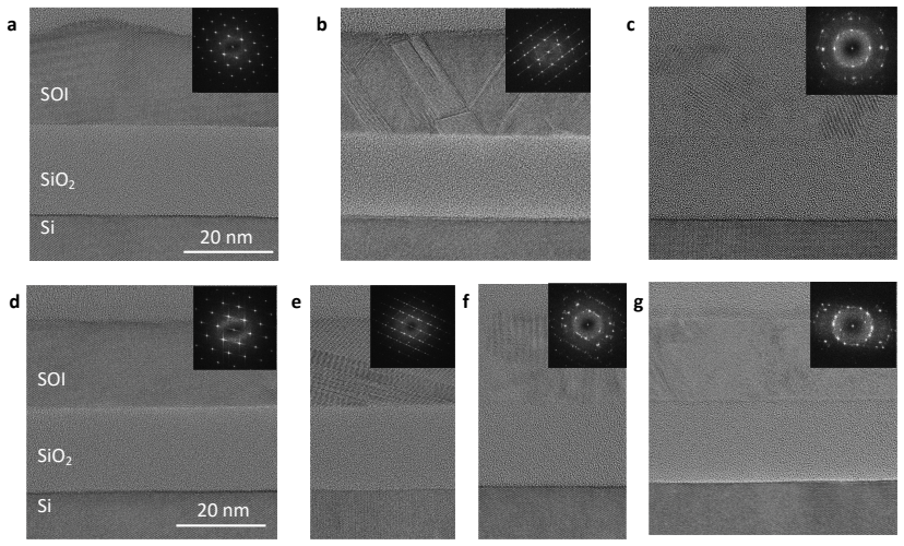
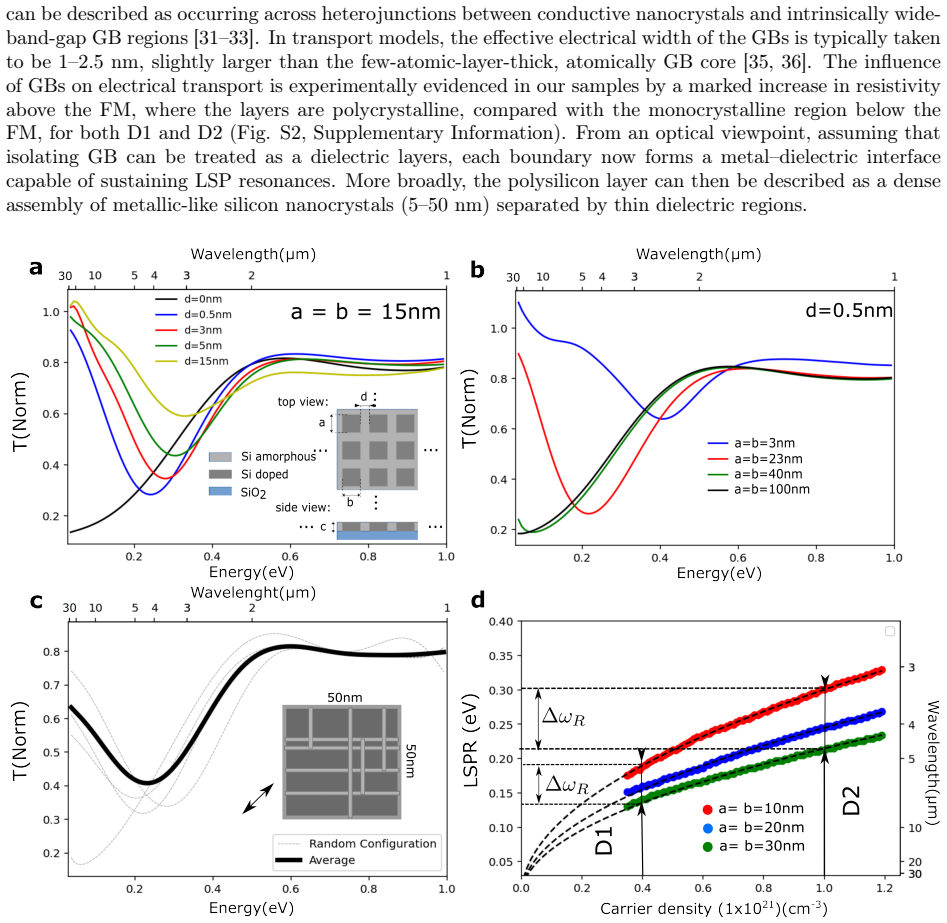
Hyperdoped polysilicon layers with nanometric grains exhibit tunable mid-infrared light-matter interactions. These properties originate from metal-dielectric interfaces at grain boundaries that support localized surface plasmon resonances, as shown by electron microscopy, infrared spectroscopy, and finite-difference time-domain simulations. The result holds for any doped semiconductor system provided the grain size stays in the nanometric range, independent of the synthesis method.
What carries the argument
Naturally formed metal-dielectric interfaces at grain boundaries in hyperdoped nanometric-grain polysilicon that support localized surface plasmon resonances.
If this is right
- Mid-infrared plasmonic responses become possible without any external nanoscale patterning.
- Resonance frequency can be tuned across the mid-infrared by adjusting hyperdoping and annealing conditions.
- The films remain fully compatible with standard microelectronic and photovoltaic fabrication flows.
- The same grain-boundary mechanism should appear in other polycrystalline doped semiconductors with nanometric grains.
Where Pith is reading between the lines
- Grain-size control during deposition could become a design variable for infrared plasmonic devices instead of lithographic patterning.
- Unexpected optical losses observed in polycrystalline semiconductor layers may partly trace to these grain-boundary resonances.
- The approach invites tests in other wavelength ranges by selecting semiconductors whose plasma frequency matches the target band.
Load-bearing premise
The measured mid-infrared optical features are specifically localized surface plasmon resonances supported by grain-boundary metal-dielectric interfaces rather than other absorption or scattering mechanisms.
What would settle it
If single-crystal hyperdoped silicon of the same doping level shows no comparable mid-IR absorption features, or if electrodynamic simulations without explicit grain-boundary interfaces fail to reproduce the measured spectra.
Figures


read the original abstract
The ability to engineer localized surface plasmon resonances at large scale usually relies on precise nanoscale patterning. Here, we demonstrate that mid-infrared plasmonic responses can instead emerge in unpatterned polysilicon films composed of nanometric (5-50 nm) grains, challenging established design paradigms and eliminating the need for external nanostructuring. Using tailored out-of-equilibrium annealing conditions, we show that hyperdoped polysilicon layers exhibit enhanced light-matter interactions that can be tuned across the mid-infrared range. By combining advanced electron microscopy, infrared spectroscopy and finite-difference time-domain electrodynamic simulations, we demonstrate that these remarkable optical properties originate from naturally formed metal-dielectric interfaces at grain boundaries, which support localized surface plasmon resonances. Importantly, this result is universal and can be extended to any doped semiconductor system, regardless of the synthesis technique, provided that the grain size remains in the nanometric range. This work opens up a new field in plasmonics centered on polycrystalline semiconductors, paving the way for cost-effective systems that are fully compatible with microelectronic and photovoltaic technologies, and capable of significantly reshaping light-matter interactions in the infrared range.
Editorial analysis
A structured set of objections, weighed in public.
Referee Report
Summary. The paper claims that mid-infrared localized surface plasmon resonances (LSPRs) emerge in unpatterned hyperdoped polycrystalline silicon films with nanometric (5-50 nm) grains, arising from naturally formed metal-dielectric interfaces at grain boundaries rather than requiring external patterning. This is supported by transmission electron microscopy for grain-size statistics, FTIR spectroscopy showing tunable mid-IR optical features, and FDTD electrodynamic simulations that reproduce the resonances when grain boundaries are modeled as metallic. The work asserts that the effect is universal to any doped semiconductor with nanometric grains and opens a new field in polycrystalline plasmonics compatible with microelectronics and photovoltaics.
Significance. If the central interpretation holds, the result would be significant for plasmonics and nanophotonics by showing that large-scale mid-IR light-matter interactions can be achieved without nanofabrication in polycrystalline semiconductors, potentially enabling cost-effective, CMOS-compatible devices. The multi-technique approach (microscopy + spectroscopy + simulations) is a strength, and the absence of free parameters in the core claim (grain boundaries as the origin) is noteworthy if the model uniqueness can be established.
major comments (3)
- [FDTD simulations and optical modeling section] The attribution of the mid-IR absorption features specifically to grain-boundary LSPRs requires demonstrating that this model is uniquely favored. However, no quantitative model-comparison (e.g., chi-squared or residual analysis) is provided showing that a homogeneous Drude model or effective-medium approximation without explicit metallic boundaries fails to fit the FTIR data at comparable quality. This is load-bearing for the central claim.
- [Experimental results and FTIR spectroscopy section] Control experiments isolating the grain-size dependence are absent. Spectra from larger-grain or single-crystal hyperdoped Si samples under identical hyperdoping conditions would be needed to confirm that the tunable mid-IR features disappear or shift when nanometric grains are not present.
- [Discussion and conclusions] The universality statement (that the result extends to any doped semiconductor with nanometric grains regardless of synthesis technique) is asserted from the polysilicon case alone. No additional material systems, theoretical scaling arguments, or grain-size threshold analysis are provided to support generalization beyond the specific hyperdoped polysilicon films studied.
minor comments (2)
- [Abstract] The abstract and introduction would benefit from explicit mention of the spectral range and peak positions observed in FTIR to allow readers to assess the mid-IR tuning claim without referring to figures.
- [Results section] Error bars or uncertainty quantification on the FTIR spectra and grain-size distributions from TEM would improve the rigor of the experimental claims.
Simulated Author's Rebuttal
We thank the referee for the constructive and detailed report. We address each major comment below with point-by-point responses, indicating where revisions will be incorporated.
read point-by-point responses
-
Referee: [FDTD simulations and optical modeling section] The attribution of the mid-IR absorption features specifically to grain-boundary LSPRs requires demonstrating that this model is uniquely favored. However, no quantitative model-comparison (e.g., chi-squared or residual analysis) is provided showing that a homogeneous Drude model or effective-medium approximation without explicit metallic boundaries fails to fit the FTIR data at comparable quality. This is load-bearing for the central claim.
Authors: We agree that a quantitative model comparison would strengthen the uniqueness argument. In the revised manuscript we will add chi-squared and residual analyses comparing the grain-boundary FDTD model against a homogeneous Drude model and an effective-medium approximation applied to the same FTIR spectra. Our existing simulations already show that only the explicit metallic boundaries reproduce the observed resonance positions and line shapes without adjustable parameters; the added metrics will make this explicit. revision: yes
-
Referee: [Experimental results and FTIR spectroscopy section] Control experiments isolating the grain-size dependence are absent. Spectra from larger-grain or single-crystal hyperdoped Si samples under identical hyperdoping conditions would be needed to confirm that the tunable mid-IR features disappear or shift when nanometric grains are not present.
Authors: We acknowledge the desirability of such controls. However, the out-of-equilibrium annealing process that produces the hyperdoped polycrystalline films inherently yields nanometric grains; single-crystal hyperdoped Si under identical doping and thermal conditions cannot be fabricated by the same route and would introduce different defect landscapes. Our evidence rests on the direct correlation between measured grain-size distributions (TEM) and resonance positions, together with simulations in which removing the boundaries eliminates the mid-IR features. We will expand the discussion to clarify this reasoning and the practical limitations on identical-condition controls. revision: no
-
Referee: [Discussion and conclusions] The universality statement (that the result extends to any doped semiconductor with nanometric grains regardless of the synthesis technique) is asserted from the polysilicon case alone. No additional material systems, theoretical scaling arguments, or grain-size threshold analysis are provided to support generalization beyond the specific hyperdoped polysilicon films studied.
Authors: The universality follows from the mechanism: metallic grain boundaries form in any doped semiconductor once grain size is nanometric, independent of material or growth method. We will revise the discussion to include a simple scaling argument based on the ratio of grain diameter to the plasma wavelength, demonstrating that resonances appear whenever grains remain much smaller than the relevant infrared wavelength. While no additional experimental systems are presented, this mechanistic scaling provides the requested theoretical support for generalization. revision: partial
Circularity Check
No circularity: experimental demonstration supported by independent measurements and modeling
full rationale
The paper's central claim rests on direct experimental observations (TEM grain-size statistics, FTIR spectra) combined with FDTD simulations that reproduce the measured resonances when grain boundaries are modeled as metallic interfaces. No derivation chain, equation, or prediction is shown that reduces by construction to quantities fitted from the same dataset. The universality assertion is presented as an extrapolation from the polysilicon case rather than a mathematical result derived from the paper's own equations. No self-citations are invoked as load-bearing uniqueness theorems, and no ansatz or renaming of known results is used to substitute for evidence. The work is self-contained against external benchmarks (microscopy images and spectra), consistent with a score of 0.
Axiom & Free-Parameter Ledger
axioms (2)
- standard math Standard electromagnetic theory and plasmonics principles apply to nanoscale grain-boundary interfaces.
- domain assumption Grain boundaries in hyperdoped polycrystalline silicon form effective metal-dielectric interfaces capable of supporting localized surface plasmons.
Reference graph
Works this paper leans on
-
[1]
The Journal of Physical Chemistry Letters , author =
Plasmon. The Journal of Physical Chemistry Letters , author =. 2014 , pages =. doi:10.1021/jz500037k , abstract =
-
[2]
Localized surface plasmon resonances arising from free carriers in doped quantum dots , volume =. Nature Materials , author =. 2011 , pages =. doi:10.1038/nmat3004 , language =
-
[3]
Plasmonic doped semiconductor nanocrystals:. Physics Reports , author =. 2017 , pages =. doi:10.1016/j.physrep.2017.01.003 , abstract =
-
[4]
Semiconductor infrared plasmonics , volume =. Nanophotonics , author =. 2019 , pages =. doi:10.1515/nanoph-2019-0077 , abstract =
-
[5]
Benchmarking the. ACS Photonics , author =. 2018 , pages =. doi:10.1021/acsphotonics.8b00438 , abstract =
-
[6]
Alternative. Advanced Materials , author =. 2013 , pages =. doi:10.1002/adma.201205076 , language =
-
[7]
Midinfrared. Nano Letters , author =. 2015 , pages =. doi:10.1021/acs.nanolett.5b03247 , abstract =
-
[8]
Intrinsic
Pichler, Peter , editor =. Intrinsic. 2004 , doi =
2004
-
[9]
The Journal of Physical Chemistry Letters , author =
Plasmons in. The Journal of Physical Chemistry Letters , author =. 2013 , pages =. doi:10.1021/jz401719u , abstract =
-
[10]
Materials Characterization , author =. 2020 , pages =. doi:10.1016/j.matchar.2020.110174 , abstract =
-
[11]
, year =
Maier, Stefan A. , year =. Plasmonics: fundamentals and applications , isbn =
-
[12]
Zeitschrift für Kristallographie , author =
Automated nanocrystal orientation and phase mapping in the transmission electron microscope on the basis of precession electron diffraction , volume =. Zeitschrift für Kristallographie , author =. 2010 , pages =. doi:10.1524/zkri.2010.1205 , abstract =
-
[13]
Towards nano-scale photonics with micro-scale photons: the opportunities and challenges of mid-infrared plasmonics , volume =. Nanophotonics , author =. 2013 , pages =. doi:10.1515/nanoph-2012-0027 , abstract =
-
[14]
Materials Science in Semiconductor Processing , author =
Doping of semiconductor devices by. Materials Science in Semiconductor Processing , author =. 2017 , pages =. doi:10.1016/j.mssp.2016.11.008 , abstract =
-
[15]
Journal of Applied Physics , author =
Study of recrystallization and activation processes in thin and highly doped silicon-on-insulator layers by nanosecond laser thermal annealing , volume =. Journal of Applied Physics , author =. 2022 , pages =. doi:10.1063/5.0073827 , abstract =
-
[16]
Plasmonic. Nano Letters , author =. 2015 , pages =. doi:10.1021/acs.nanolett.5b02287 , abstract =
-
[17]
Hyper-. ACS Photonics , author =. 2021 , pages =. doi:10.1021/acsphotonics.1c00019 , abstract =
-
[18]
ACS Applied Nano Materials , author =
Heavily. ACS Applied Nano Materials , author =. 2023 , pages =. doi:10.1021/acsanm.2c05088 , abstract =
-
[19]
Infrared nanoplasmonic properties of hyperdoped embedded. Nanophotonics , author =. 2022 , pages =. doi:10.1515/nanoph-2022-0283 , abstract =
-
[20]
Comparative. ACS Nano , author =. 2015 , note =. doi:10.1021/nn505416r , abstract =
-
[21]
Optics Communications , author =
Optical properties of two interacting gold nanoparticles , volume =. Optics Communications , author =. 2003 , pages =. doi:10.1016/S0030-4018(03)01357-9 , abstract =
-
[22]
Interparticle. Nano Letters , author =. 2003 , pages =. doi:10.1021/nl034197f , abstract =
-
[23]
Observation of near-field coupling in metal nanoparticle chains using far-field polarization spectroscopy , volume =. Physical Review B , author =. 2002 , pages =. doi:10.1103/PhysRevB.65.193408 , language =
-
[24]
The Journal of Physical Chemistry B , author =
Confined. The Journal of Physical Chemistry B , author =. 2005 , pages =. doi:10.1021/jp049084e , language =
-
[25]
MATERIALS TRANSACTIONS , author =
Atomic. MATERIALS TRANSACTIONS , author =. 2007 , pages =. doi:10.2320/matertrans.MD200706 , language =
-
[26]
IEEE Transactions on Electron Devices , author =
Theory of conduction in polysilicon:. IEEE Transactions on Electron Devices , author =. 1984 , pages =. doi:10.1109/T-ED.1984.21554 , abstract =
-
[27]
Kamins, Ted. Electrical Properties. Polycrystalline Silicon for Integrated Circuits and Displays. 1998. doi:10.1007/978-1-4615-5577-3_5
-
[28]
Progress in Materials Science , author =
Plasmonic metasurfaces:. Progress in Materials Science , author =. 2025 , pages =. doi:10.1016/j.pmatsci.2025.101508 , abstract =
-
[29]
International Journal of Precision Engineering and Manufacturing-Green Technology , author =
Cost-. International Journal of Precision Engineering and Manufacturing-Green Technology , author =. 2024 , pages =. doi:10.1007/s40684-023-00580-x , abstract =
-
[30]
Proceedings of the National Academy of Sciences , author =
Criticality of metals and metalloids , volume =. Proceedings of the National Academy of Sciences , author =. 2015 , pages =. doi:10.1073/pnas.1500415112 , abstract =
-
[31]
Plasmonic and. Applied Sciences , author =. 2016 , pages =. doi:10.3390/app6090239 , abstract =
-
[32]
Journal of Applied Physics , author =
Infrared surface plasmons on heavily doped silicon , volume =. Journal of Applied Physics , author =. 2011 , pages =. doi:10.1063/1.3672738 , abstract =
-
[33]
Journal of Semiconductors , author =
Heavily doped silicon:. Journal of Semiconductors , author =. 2021 , pages =. doi:10.1088/1674-4926/42/6/062302 , abstract =
-
[34]
Materials Science and Engineering: A , author =
Interfacial state and potential barrier height associated with grain boundaries in polycrystalline silicon , volume =. Materials Science and Engineering: A , author =. 2007 , pages =. doi:10.1016/j.msea.2006.02.471 , abstract =
-
[35]
IEEE Transactions on Electron Devices , author =
A model for conduction in polycrystalline silicon&\#8212. IEEE Transactions on Electron Devices , author =. 1981 , pages =. doi:10.1109/T-ED.1981.20504 , abstract =
-
[36]
Frontiers in Physics , author =
A. Frontiers in Physics , author =. 2021 , pages =. doi:10.3389/fphy.2020.586087 , abstract =
-
[37]
Optical. Chemical Reviews , author =. 2022 , pages =. doi:10.1021/acs.chemrev.2c00078 , abstract =
-
[38]
Materials Science Reports , author =
Kinetics of solid phase crystallization in amorphous silicon , volume =. Materials Science Reports , author =. 1988 , pages =. doi:10.1016/S0920-2307(88)80005-7 , language =
-
[39]
Plasmonic meta-atoms and metasurfaces , volume =. Nature Photonics , author =. 2014 , pages =. doi:10.1038/nphoton.2014.247 , language =
-
[40]
and Fundenberger,J
Beausir, B. and Fundenberger,J. J. , title =
-
[41]
Computer Physics Communications , volume=
MEEP: A flexible free-software package for electromagnetic simulations by the FDTD method , author=. Computer Physics Communications , volume=. 2010 , publisher=
2010
-
[42]
Applied Surface Science , author =
Formation of polycrystalline silicon with log-normal grain size distribution , volume =. Applied Surface Science , author =. 1998 , pages =. doi:10.1016/S0169-4332(97)00494-7 , abstract =
-
[43]
Challenges in nanofabrication for efficient optical metasurfaces , volume =. Scientific Reports , author =. 2021 , pages =. doi:10.1038/s41598-021-84666-z , abstract =
-
[44]
Hyperdoped. Nanoscale , author =. 2023 , pages =. doi:10.1039/D3NR00035D , abstract =
discussion (0)
Sign in with ORCID, Apple, or X to comment. Anyone can read and Pith papers without signing in.