Recognition: unknown
Si/SiGe multi-channel superlattice structure epitaxial growth with segmented temperature control for Next-Generation Logic Devices
Pith reviewed 2026-05-08 08:52 UTC · model grok-4.3
The pith
Segmented temperature control during epitaxial growth reduces Ge diffusion in Si/SiGe superlattices to 5.6-7% of its 650C value, preserving sharp interfaces and coherent strain in an 8-channel stack.
A machine-rendered reading of the paper's core claim, the machinery that carries it, and where it could break.
Core claim
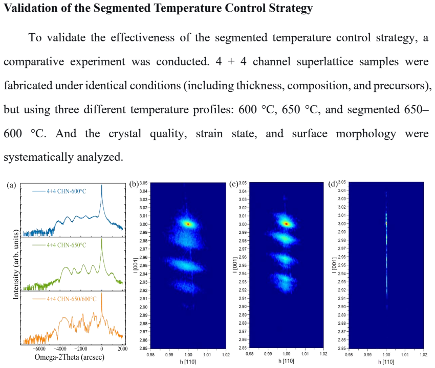
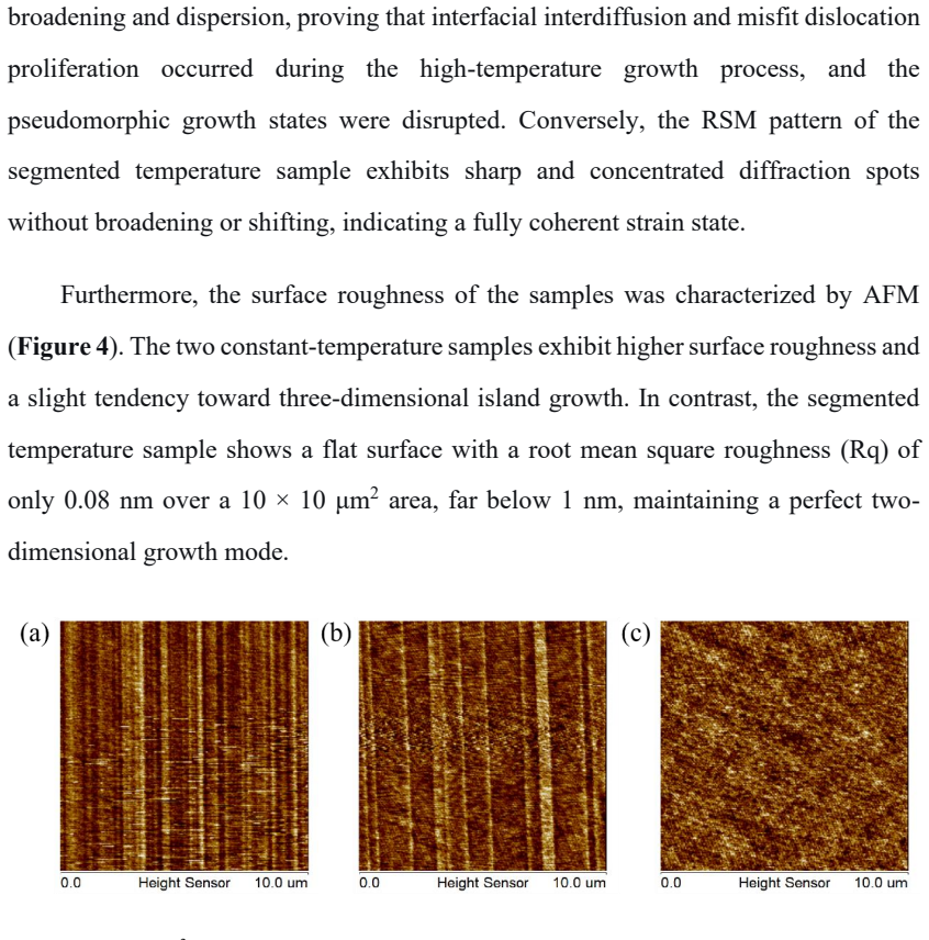
The authors claim that segmented temperature control during epitaxial growth of Si/SiGe multi-channel superlattices lowers the Ge diffusion coefficient to 5.6-7% of its value at 650C, thereby suppressing interdiffusion and maintaining pseudomorphic strain. The 4+4 channel stack exhibits clear XRD satellite peaks, a fully coherent strain state via reciprocal space mapping, sharp interfaces with 1.5-2.6 nm transition widths, and low RMS roughness of 0.08 nm. Bottom-to-top quantitative analysis shows that prolonged high-temperature exposure broadens lower interfaces and dilutes Ge concentration from 20% to 18.5%, while upper layers stay close to design targets, supplying process-physics insight
What carries the argument
Segmented temperature control applied during epitaxial growth, which shortens high-temperature dwell times to reduce the time-integrated Ge diffusion coefficient and thereby limit Si-Ge interdiffusion across the superlattice periods.
If this is right
- The 4+4 channel stack maintains a fully coherent strain state without relaxation as verified by reciprocal space mapping.
- Interfaces remain sharp with transition widths of 1.5-2.6 nm and surface roughness of 0.08 nm RMS across the stack.
- Lower channels experience measurable broadening and slight Ge dilution from cumulative thermal exposure while upper channels match design specifications.
- The method supplies a high-quality material platform for fabricating logic devices at nodes beyond 2 nm.
Where Pith is reading between the lines
- Further refinement of the temperature segment durations or peak values could support stacks with more than eight channels while keeping all layers within target specifications.
- The same segmented-control principle may apply to other diffusion-sensitive heterostructures, such as different group-IV or III-V superlattices used in optoelectronics or quantum devices.
- Pairing this growth technique with lower-temperature surface preparation steps could reduce the small bottom-to-top gradient still observed in the current 4+4 stack.
Load-bearing premise
The standard Arrhenius model for the Ge diffusion coefficient accurately describes the reduction achieved by the specific temperature segments, with no extra interdiffusion or defects introduced by the temperature cycling itself.
What would settle it
Secondary ion mass spectrometry or transmission electron microscopy profiles of the 4+4 stack that show interface transition widths larger than 3 nm, Ge concentration dilution exceeding the predicted amount in upper layers, or reciprocal space mapping indicating partial strain relaxation would falsify the claimed suppression of interdiffusion.
Figures

read the original abstract
Stacking multiple SiSiGe channels in advanced logic devices faces severe thermal budget accumulation, which degrades interfaces via Ge-Si interdiffusion and strain relaxation.This strategy lowers the Ge diffusion coefficient to 5.6-7% of its value at 650C (Arrhenius estimate), suppressing interdiffusion and preserving pseudomorphic strain. The 4 + 4 channel stack exhibits clear XRD satellite peaks, fully coherent strain state (reciprocal space mapping), sharp interfaces (1.5-2.6 nm transition width) and low RMS roughness (0.08 nm). Quantitative analysis from bottom to top reveals that prolonged high-temperature exposure broadens bottom interfaces and dilutes Ge concentration (from 20% to 18.5%), while the top stack maintains design targets. This work provides a process-physics understanding of thermal budget effects in multi-channel superlattices and establishes a high-quality material foundation for advanced logic devices beyond 2 nm node.
Editorial analysis
A structured set of objections, weighed in public.
Referee Report
Summary. The manuscript presents an epitaxial growth process for a Si/SiGe 4+4 channel superlattice using segmented temperature control to manage thermal budget accumulation. This is claimed to reduce the effective Ge diffusion coefficient to 5.6-7% of its 650°C value via an Arrhenius estimate, thereby suppressing interdiffusion, preserving pseudomorphic strain, and yielding sharp interfaces (1.5-2.6 nm transition widths), low RMS roughness (0.08 nm), clear XRD satellite peaks, and fully coherent strain via reciprocal space mapping. Bottom-to-top analysis shows Ge dilution (20% to 18.5%) and broadening in lower layers while upper layers meet targets.
Significance. If the segmented temperature approach and diffusion reduction hold, the work provides a practical route to higher-channel-count superlattices for logic devices beyond the 2 nm node while maintaining interface quality and strain. The reported XRD, RSM, and roughness data are standard and high-quality, supporting the structural claims and offering process-physics insights into thermal budget effects in multi-channel stacks.
major comments (2)
- Abstract: The claim that segmented temperature control reduces the Ge diffusion coefficient to 5.6-7% of the 650°C value rests on an approximate Arrhenius estimate using literature activation energy, without reported error bars, explicit profile integration details, or direct diffusion measurements. This estimate is load-bearing for the central assertion of suppressed interdiffusion and preserved strain.
- Abstract: The observed bottom-to-top variation (Ge dilution from 20% to 18.5% and interface broadening in lower layers due to prolonged high-temperature exposure) is not quantitatively compared against the predicted 5.6-7% reduction; if the degradation exceeds the Arrhenius prediction, the effectiveness for multi-channel stacks and the process understanding are incomplete.
minor comments (2)
- The specific segmented temperature profile parameters (temperatures, durations, and ramp rates) are not detailed, limiting reproducibility and independent verification of the Arrhenius integral.
- Error bars or uncertainties should be reported on the interface transition widths, Ge concentrations, and roughness values to strengthen the quantitative claims.
Simulated Author's Rebuttal
We thank the referee for the positive evaluation of our work's significance and the detailed comments, which help improve the clarity of our claims regarding the segmented temperature control approach. We provide point-by-point responses to the major comments below.
read point-by-point responses
-
Referee: Abstract: The claim that segmented temperature control reduces the Ge diffusion coefficient to 5.6-7% of the 650°C value rests on an approximate Arrhenius estimate using literature activation energy, without reported error bars, explicit profile integration details, or direct diffusion measurements. This estimate is load-bearing for the central assertion of suppressed interdiffusion and preserved strain.
Authors: We agree that the diffusion reduction is derived from an Arrhenius estimate based on literature activation energy rather than direct measurement. In the revised manuscript, we will add explicit details on the calculation in the methods and supplementary information, including the integration of the segmented time-temperature profile to obtain the effective diffusion coefficient. Error bars will be incorporated using the typical uncertainty range for the Ge-Si interdiffusion activation energy from the cited literature. We will also revise the abstract to describe this as an estimate based on the reduced thermal budget. Direct diffusion measurements on dedicated test structures were outside the scope of this study focused on the 4+4 stack characterization, but the observed interface quality and strain data are consistent with suppressed diffusion. revision: yes
-
Referee: Abstract: The observed bottom-to-top variation (Ge dilution from 20% to 18.5% and interface broadening in lower layers due to prolonged high-temperature exposure) is not quantitatively compared against the predicted 5.6-7% reduction; if the degradation exceeds the Arrhenius prediction, the effectiveness for multi-channel stacks and the process understanding are incomplete.
Authors: We concur that a quantitative comparison is needed to fully validate the process understanding. The revised manuscript will include a new analysis section (or supplementary note) that calculates the expected Ge diffusion length and interface broadening for the bottom layers using the 5.6-7% reduced coefficient integrated over their longer cumulative thermal exposure, then directly compares these predictions to the measured Ge dilution (20% to 18.5%) and transition widths from TEM. This will demonstrate that the observed degradation aligns with or is below the Arrhenius-based prediction, supporting the effectiveness for higher channel counts. revision: yes
Circularity Check
No circularity: experimental report relies on direct measurements and standard Arrhenius application
full rationale
This is an experimental materials science paper on epitaxial growth of Si/SiGe multi-channel superlattices using segmented temperature control. All primary claims (XRD satellite peaks, coherent strain via RSM, interface transition widths of 1.5-2.6 nm, RMS roughness of 0.08 nm, bottom-to-top Ge dilution from 20% to 18.5%) rest on direct characterization data rather than any mathematical derivation chain. The single quantitative estimate—that segmented temperatures lower the effective Ge diffusion coefficient to 5.6-7% of the 650°C value—is a direct, non-fitted application of the standard Arrhenius equation using literature activation energy to the reported time-temperature profile; it is not derived from the paper's own data, not presented as a 'prediction' of measured outcomes, and does not rely on self-citations or prior author work for uniqueness. No equations, ansatzes, or load-bearing premises reduce to self-definition or fitted inputs. The work is self-contained against external benchmarks and exhibits no circular steps.
Axiom & Free-Parameter Ledger
free parameters (1)
- Segmented temperature profile and durations
axioms (1)
- domain assumption Ge diffusion in Si/SiGe obeys the Arrhenius equation with literature activation energy
Reference graph
Works this paper leans on
-
[1]
PPAC of sheet-based CFET configurations for 4 track design with 16nm metal pitch,
P. Schuddinck et al., “PPAC of sheet-based CFET configurations for 4 track design with 16nm metal pitch,” in 2022 IEEE Symposium on VLSI Technology and Circuits (VLSI Technology and Circuits), IEEE, 2022, pp. 365–366
2022
-
[2]
Demonstration of 3D sequential FD -SOI on CMOS FinFET stacking featuring low temperature Si layer transfer and top tier device fabrication with tier interconnections,
A. V andooren et al., “Demonstration of 3D sequential FD -SOI on CMOS FinFET stacking featuring low temperature Si layer transfer and top tier device fabrication with tier interconnections,” in 2022 IEEE Symposium on VLSI Technology and Circuits (VLSI Technology and Circuits), IEEE, 2022, pp. 330–331
2022
-
[3]
3D stacked devices and MOL innovations for post -nanosheet CMOS scaling,
N. Horiguchi et al., “3D stacked devices and MOL innovations for post -nanosheet CMOS scaling,” in 2023 International Electron Devices Meeting (IEDM), IEEE, 2023, pp. 1–4
2023
-
[4]
Z. Tao, L. Zhang, E. Dupuy, B. T. Chan, E. Altamirano-Sánchez, and F. Lazzarino, “FEOL dry etch process challenges of ultimate FinFET scaling and next generation device architectures beyond N3,” in Advanced Etch Technology for Nanopatterning IX, C. B. Labelle and R. S. Wise, Eds., San Jose, United States: SPIE, Mar. 2020, p. 24. doi: 10.1117/12.2552022
-
[5]
C. Porret et al. , “V ery Low Temperature Epitaxy of Group -IV Semiconductors for Use in FinFET, Stacked Nanowires and Monolithic 3D Integration,” ECS J. Solid State Sci. Technol., vol. 8, no. 8, pp. P392–P399, 2019, doi: 10.1149/2.0071908jss
-
[6]
The Complementary FET (CFET) for CMOS scaling beyond N3,
J. Ryckaert et al., “The Complementary FET (CFET) for CMOS scaling beyond N3,” in 2018 IEEE Symposium on VLSI Technology, Jun. 2018, pp. 141–142. doi: 10.1109/VLSIT.2018.8510618
-
[7]
Stacked nanosheet gate -all-around transistor to enable scaling beyond FinFET,
N. Loubet et al. , “Stacked nanosheet gate -all-around transistor to enable scaling beyond FinFET,” in 2017 Symposium on VLSI Technology , Jun. 2017, pp. T230 –T231. doi: 10.23919/VLSIT.2017.7998183
-
[8]
First Monolithic Integration of 3D Complementary FET (CFET) on 300mm Wafers,
S. Subramanian et al., “First Monolithic Integration of 3D Complementary FET (CFET) on 300mm Wafers,” in 2020 IEEE Symposium on VLSI Technology , Jun. 2020, pp. 1 –2. doi: 10.1109/VLSITechnology18217.2020.9265073
-
[9]
S. Liao et al., “Complementary Field-Effect Transistor (CFET) Demonstration at 48nm Gate Pitch for Future Logic Technology Scaling,” in 2023 International Electron Devices Meeting (IEDM), San Francisco, CA, USA: IEEE, Dec. 2023, pp. 1 –4. doi: 10.1109/iedm45741.2023.10413672
-
[10]
M. Kobrinsky et al., “Process Innovations for Future Technology Nodes with Back-Side Power Delivery and 3D Device Stacking,” in 2023 International Electron Devices Meeting (IEDM), Dec. 2023, pp. 1–4. doi: 10.1109/IEDM45741.2023.10413882
-
[11]
Enabling sub-5nm CMOS technology scaling thinner and taller!,
J. Ryckaert et al., “Enabling sub-5nm CMOS technology scaling thinner and taller!,” in 2019 IEEE International Electron Devices Meeting (IEDM), IEEE, 2019, p. 29.4. 1-29.4. 4
2019
-
[12]
Process and packaging innovations for Moore’s law continuation and beyond,
R. Chau, “Process and packaging innovations for Moore’s law continuation and beyond,” in 2019 IEEE International Electron Devices Meeting (IEDM), IEEE, 2019, p. 1.1. 1-1.1. 6
2019
-
[13]
Scaling below 3nm node: the 3D CMOS integration paradigm (Conference Presentation),
J. Ryckaert, “Scaling below 3nm node: the 3D CMOS integration paradigm (Conference Presentation),” in Advanced Etch Technology for Nanopatterning VIII, SPIE, 2019, p. 109630O
2019
-
[14]
Challenges and approaches in advanced Fin patterning,
L. Zhang, D. Hellin, and E. Altamirano Sanchez, “Challenges and approaches in advanced Fin patterning,” 2019
2019
-
[15]
3-D Self-aligned Stacked NMOS-on-PMOS Nanoribbon Transistors for Continued Moore’s Law Scaling,
C.-Y . Huang et al., “3-D Self-aligned Stacked NMOS-on-PMOS Nanoribbon Transistors for Continued Moore’s Law Scaling,” in 2020 IEEE International Electron Devices Meeting (IEDM), San Francisco, CA, USA: IEEE, Dec. 2020, p. 20.6.1 -20.6.4. doi: 10.1109/IEDM13553.2020.9372066
-
[16]
Epitaxial Si/SiGe Multi-Stacks: From Stacked Nano -Sheet to Fork-Sheet and CFET Devices,
R. Loo et al., “Epitaxial Si/SiGe Multi-Stacks: From Stacked Nano -Sheet to Fork-Sheet and CFET Devices,” ECS J. Solid State Sci. Technol. , vol. 14, no. 1, p. 015003, Jan. 2025, doi: 10.1149/2162-8777/ada79f
-
[17]
Epitaxial growth of active Si on top of SiGe etch stop layer in view of 3D device integration,
R. Loo et al., “Epitaxial growth of active Si on top of SiGe etch stop layer in view of 3D device integration,” ECS J. Solid State Sci. Technol., vol. 10, no. 1, p. 014001, 2021
2021
-
[18]
D. Kohen, V . D’Costa, N. Bhargava, and J. Tolle, “Abrupt SiGe-to-Si interface: influence of chemical vapor deposition processes and characterization by different metrology techniques,” Semicond. Sci. Technol., vol. 33, no. 10, p. 104003, Oct. 2018, doi: 10.1088/1361-6641/aadb83
-
[19]
Q. Zhang et al., “Influence of Rapid Thermal Annealing on Ge -Si Interdiffusion in Epitaxial Multilayer Ge 0.3 Si0.7 /Si Superlattices with Various GeSi Thicknesses,” ECS J. Solid State Sci. Technol., vol. 7, no. 11, pp. P671–P676, 2018, doi: 10.1149/2.0241811jss
-
[20]
S. Jung, D. Yoon, S. Oh, H. Shin, J. Kim, and D.-H. Ko, “Study on the interfaces between Si and SiGe in the epitaxial in-situ Boron-Doped SiGe/Si layers treated with H or Cl,” Appl. Surf. Sci., vol. 690, p. 162553, May 2025, doi: 10.1016/j.apsusc.2025.162553
-
[21]
Z. Kong et al., “Interface Investigation on SiGe/Si Multilayer Structures: Influence of Different Epitaxial Process Conditions,” ACS Appl. Mater. Interfaces, vol. 15, no. 48, pp. 56567–56574, Dec. 2023, doi: 10.1021/acsami.3c14168
-
[22]
SiGe growth kinetics and doping in reduced pressure -chemical vapor deposition,
J. M. Hartmann et al., “SiGe growth kinetics and doping in reduced pressure -chemical vapor deposition,” J. Cryst. Growth, vol. 236, no. 1–3, pp. 10–20, 2002
2002
-
[23]
A Benchmark of 300mm RP-CVD Chambers for the Low Temperature Epitaxy of Si and SiGe,
J.-M. Hartmann, V . Mazzocchi, F. Pierre, and J.-P. Barnes, “A Benchmark of 300mm RP-CVD Chambers for the Low Temperature Epitaxy of Si and SiGe,” ECS Trans., vol. 86, no. 7, pp. 219– 231, Jul. 2018, doi: 10.1149/08607.0219ecst
-
[24]
Low temperature Si homo-epitaxy by reduced pressure chemical vapor deposition using dichlorosilane, silane and trisilane,
B. Vincent, R. Loo, W. Vandervorst, G. Brammertz, and M. Caymax, “Low temperature Si homo-epitaxy by reduced pressure chemical vapor deposition using dichlorosilane, silane and trisilane,” J. Cryst. Growth, vol. 312, no. 19, pp. 2671–2676, 2010
2010
-
[25]
TEM investigations of gate -all-around nanowire devices,
P. Favia et al. , “TEM investigations of gate -all-around nanowire devices,” Semicond. Sci. Technol., vol. 34, no. 12, p. 124003, 2019
2019
-
[26]
Semiconductor profiling with sub-nm resolution: Challenges and solutions,
W. Vandervorst, “Semiconductor profiling with sub-nm resolution: Challenges and solutions,” Appl. Surf. Sci., vol. 255, no. 4, pp. 805–812, 2008
2008
-
[27]
Ge Self-Diffusion in Epitaxial Si 1 − x Ge x Layers,
N. R. Zangenberg, J. Lundsgaard Hansen, J. Fage -Pedersen, and A. Nylandsted Larsen, “Ge Self-Diffusion in Epitaxial Si 1 − x Ge x Layers,” Phys. Rev. Lett., vol. 87, no. 12, p. 125901, Aug. 2001, doi: 10.1103/PhysRevLett.87.125901
-
[28]
Dependence of critical thickness on growth temperature in Ge x Si1− x/Si superlattices,
R. H. Miles et al., “Dependence of critical thickness on growth temperature in Ge x Si1− x/Si superlattices,” Appl. Phys. Lett., vol. 52, no. 11, pp. 916–918, 1988
1988
-
[29]
Critical thickness for plastic relaxation of SiGe on Si (001) revisited,
J. M. Hartmann, A. Abbadie, and S. Favier, “Critical thickness for plastic relaxation of SiGe on Si (001) revisited,” J. Appl. Phys., vol. 110, no. 8, 2011
2011
-
[30]
Accurate quantification of Si/SiGe interface profiles via atom probe tomography,
O. Dyck et al. , “Accurate quantification of Si/SiGe interface profiles via atom probe tomography,” Adv. Mater. Interfaces, vol. 4, no. 21, p. 1700622, 2017
2017
discussion (0)
Sign in with ORCID, Apple, or X to comment. Anyone can read and Pith papers without signing in.