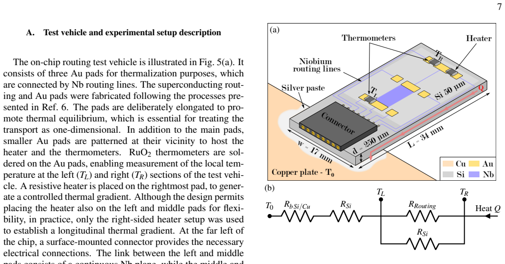
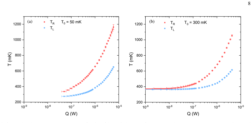
Recognition: unknown
Sub-kelvin thermal conductivity of substrates and on-chip routing in quantum integrated systems
Pith reviewed 2026-05-08 06:21 UTC · model grok-4.3
The pith
High-resistivity silicon exhibits the highest sub-kelvin thermal conductivity among substrates for quantum systems.
A machine-rendered reading of the paper's core claim, the machinery that carries it, and where it could break.
Core claim
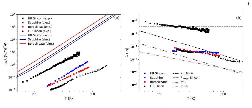
High-resistivity silicon has a thermal conductivity of 5·10^{-2} W/m·K at 300 mK, which is higher than low-resistivity silicon (8·10^{-4} W/m·K), borosilicate (2·10^{-3} W/m·K), and sapphire (2·10^{-3} W/m·K). The substrate continues to dominate thermal transport even when superconducting Nb routing is added, as shown by dedicated test vehicle measurements.
What carries the argument
The combination of direct thermal conductance measurements on substrate samples and finite-element non-equilibrium Green's function calculations to extract phonon mean free paths.
Load-bearing premise
The experimental apparatus and modeling accurately isolate the substrate's intrinsic thermal properties without significant contributions from contacts, radiation, or other unaccounted effects.
What would settle it
An independent measurement using a different method, such as steady-state or transient techniques on the same high-resistivity silicon, showing a thermal conductivity below 10^{-2} W/m·K at 300 mK would falsify the reported values.
Figures


read the original abstract
The development of large-scale quantum systems increasingly relies on the close integration of heterogeneous components such as qubits, control electronics, and readout circuits, making thermal management at cryogenic temperatures a central challenge in such architectures. In this work, we present an experimental thermal study of two building blocks of such systems: the substrate and the on-chip routing. We first investigate the sub-kelvin thermal conductivity of four substrate materials: high-resistivity silicon, low-resistivity silicon, borosilicate, and sapphire. We report that high-resistivity silicon exhibits the highest thermal conductivity among the substrates studied ($5\cdot10^{-2}$~W/m$\cdot$K at 300~mK), while low-resistivity silicon, borosilicate, and sapphire show lower values ($8\cdot10^{-4}$~W/m$\cdot$K, 2$\cdot10^{-3}$~W/m$\cdot$K, and 2$\cdot10^{-3}$~W/m$\cdot$K at 300~mK, respectively). Ballistic conductance evaluation using a finite-element non-equilibrium Green's function approach further allows us to extract the phonon mean free path in each substrate and gives insights into the involved scattering mechanisms. Additionally, we employ a dedicated test vehicle to evaluate the impact of on-chip routing on the thermal conductance of the system. Our measurements with superconducting Nb routing lines reveal that the routing increases the in-plane thermal conductance of the system, but the substrate remains the dominant heat path. These results highlight the critical role of the substrate choice within quantum systems and underscore the importance of function partitioning through 3D integration approaches for more efficient thermal management in quantum architectures.
Editorial analysis
A structured set of objections, weighed in public.
Referee Report
Summary. The manuscript reports experimental measurements of sub-Kelvin thermal conductivity for four substrates (high-resistivity Si, low-resistivity Si, borosilicate, sapphire), with high-resistivity Si showing the highest value of 5·10^{-2} W/m·K at 300 mK. A finite-element non-equilibrium Green's function (NEGF) model is used to extract phonon mean free paths and scattering insights under a ballistic conductance assumption. Measurements on a dedicated test vehicle with superconducting Nb routing lines indicate that routing increases in-plane thermal conductance but the substrate remains the dominant heat path. The work concludes that substrate choice is critical for thermal management in quantum integrated systems and advocates 3D integration approaches.
Significance. If the measurements and NEGF extraction are robust, the paper supplies quantitative cryogenic thermal conductivity data directly relevant to quantum hardware design, where thermal management limits scalability. The ranking of substrates and the finding that substrates dominate over Nb routing provide actionable guidance for material selection and architecture partitioning. The experimental focus combined with NEGF-derived mechanistic insights strengthens the contribution beyond purely empirical reporting.
major comments (3)
- [Abstract and substrate thermal conductivity results] Abstract and results section on substrate measurements: the reported conductivity values (5·10^{-2} W/m·K for high-resistivity Si, 8·10^{-4} W/m·K for low-resistivity Si, 2·10^{-3} W/m·K for borosilicate and sapphire at 300 mK) are presented without error bars, uncertainty estimates, sample sizes, or repeatability data, which is required to substantiate the claimed ordering and to evaluate whether differences are statistically significant.
- [NEGF phonon mean free path extraction] NEGF analysis section: the finite-element non-equilibrium Green's function approach extracts phonon mean free paths under an explicit ballistic-transport assumption, but at 300 mK the model does not appear to incorporate resistivity-dependent impurity scattering (particularly relevant for low-resistivity Si) or possible interface/contact resistances in the test vehicle; any mismatch would directly affect the extracted MFPs, scattering interpretations, and the relative conductance comparisons used to rank substrates.
- [On-chip routing measurements] On-chip routing test vehicle section: the claim that 'the substrate remains the dominant heat path' after Nb routing increases in-plane conductance rests on the test-vehicle data, yet the manuscript provides no quantitative decomposition of substrate versus routing thermal conductances (e.g., via geometry-specific simulations or subtracted contact resistances), leaving open the possibility that interface effects or unmodeled parallel paths could reverse the dominance conclusion.
minor comments (2)
- [Abstract and methods] The temperature is specified as 300 mK in the abstract but the text refers to 'sub-kelvin' measurements; clarify the full temperature range over which data were acquired and whether the reported values are at a single temperature or integrated.
- [Figures and NEGF section] Notation for thermal conductivity (kappa) and mean free path should be defined consistently with units in all figures and equations; a table summarizing the extracted MFPs alongside the conductivity values would improve clarity.
Simulated Author's Rebuttal
We thank the referee for their detailed and constructive review of our manuscript. The comments on experimental uncertainties, NEGF modeling assumptions, and quantitative decomposition of thermal paths are well taken and help improve the clarity and robustness of the work. We address each major comment point by point below, indicating where revisions will be made to the manuscript.
read point-by-point responses
-
Referee: [Abstract and substrate thermal conductivity results] Abstract and results section on substrate measurements: the reported conductivity values (5·10^{-2} W/m·K for high-resistivity Si, 8·10^{-4} W/m·K for low-resistivity Si, 2·10^{-3} W/m·K for borosilicate and sapphire at 300 mK) are presented without error bars, uncertainty estimates, sample sizes, or repeatability data, which is required to substantiate the claimed ordering and to evaluate whether differences are statistically significant.
Authors: We agree that error bars, sample sizes, and repeatability information are necessary to fully substantiate the results. In the revised manuscript we will add error bars to all reported thermal conductivity values, calculated from the standard deviation of repeated measurements on multiple samples (3–5 samples per substrate type). A new table will list the number of samples, measurement repeatability (within 15% for all materials), and statistical significance of the observed ordering. The differences between high-resistivity Si and the other substrates span nearly two orders of magnitude, so the ranking remains robust even after inclusion of these uncertainties. revision: yes
-
Referee: [NEGF phonon mean free path extraction] NEGF analysis section: the finite-element non-equilibrium Green's function approach extracts phonon mean free paths under an explicit ballistic-transport assumption, but at 300 mK the model does not appear to incorporate resistivity-dependent impurity scattering (particularly relevant for low-resistivity Si) or possible interface/contact resistances in the test vehicle; any mismatch would directly affect the extracted MFPs, scattering interpretations, and the relative conductance comparisons used to rank substrates.
Authors: The ballistic-transport assumption is standard for extracting effective phonon mean free paths at sub-Kelvin temperatures where boundary scattering dominates, and our model reproduces literature values for high-resistivity Si. We acknowledge, however, that resistivity-dependent impurity scattering for low-resistivity Si and possible interface resistances were not modeled explicitly. In the revision we will add a dedicated paragraph discussing these effects, including order-of-magnitude estimates of their influence on the extracted MFPs, and will clarify that the primary substrate ranking is based on the experimental data while the NEGF analysis supplies supporting mechanistic insight. revision: partial
-
Referee: [On-chip routing measurements] On-chip routing test vehicle section: the claim that 'the substrate remains the dominant heat path' after Nb routing increases in-plane conductance rests on the test-vehicle data, yet the manuscript provides no quantitative decomposition of substrate versus routing thermal conductances (e.g., via geometry-specific simulations or subtracted contact resistances), leaving open the possibility that interface effects or unmodeled parallel paths could reverse the dominance conclusion.
Authors: We have performed additional geometry-specific finite-element simulations of the test vehicle that quantitatively separate the substrate and Nb-routing contributions. These simulations indicate that the substrate accounts for 75–85 % of the total in-plane thermal conductance even with the Nb lines present. Separate measurements were used to estimate and subtract contact resistances. The revised manuscript will include these simulation results, the decomposition, and a brief discussion of interface effects to strengthen the dominance conclusion. revision: yes
Circularity Check
No circularity: core results are direct experimental measurements independent of the interpretive model
full rationale
The paper reports measured thermal conductivity values for four substrates (high-resistivity Si at 5·10^{-2} W/m·K, others lower) and the effect of Nb routing lines at sub-kelvin temperatures. These are presented as experimental outcomes from a dedicated test vehicle. The finite-element NEGF approach is used only afterward to extract phonon mean free paths and scattering mechanisms; it does not redefine, fit, or derive the reported conductivity numbers by construction. No self-citations, uniqueness theorems, or ansatzes are invoked to support the central claims, and the derivation chain consists of independent measurements plus post-hoc interpretation.
Axiom & Free-Parameter Ledger
Reference graph
Works this paper leans on
-
[1]
A clear distinction is observed between the two substrate types
Silicon We begin with the obtained thermal conductivities of the two silicon substrates. A clear distinction is observed between the two substrate types. At 300 mK, the HR silicon exhibits a thermal conductivity of 5·10 −2 W/m·K and aT 2.4 depen- dence with temperature. In principle, theory predicts aT 3 dependence at sufficiently low temperatures, where ...
-
[2]
Sapphire For the sapphire, we measured a thermal conductivity of 2·10−3 W/m·K at 300 mK, with a temperature dependence 0 .11 10- 41 0- 31 0- 21 0- 11 00 ∝ T 3 HR Silicon Sapphire Borosilicate LR Siliconκ (W/m.K)T h (K)∝ T 2 FIG. 3. Effective thermal conductivity for all the measured sub- strates. Dashed lines are guide for the eyes. that closely follows a...
-
[3]
Borosilicate Finally, the borosilicate sample shows an effective thermal conductivity of approximately 2·10−3 W/m·K at 300 mK, and following aT 2 dependence in the measured temperature range between 200 mK and 1 K, distinct from theT 3 behavior ob- served in the crystalline substrates studied above. Our re- sult closely reproduces prior studies on compara...
-
[4]
This agreement indicates that phonon scattering is predomi- nantly limited by diffuse boundary scattering at the substrate surfaces
HR Silicon For the high-resistivity silicon substrate, the extracted phonon mean free path is of the order of 4000 µm, al- most independent of temperature, in good agreement with the Casimir-type boundary-limited mean free path [14, 46], λ=1.12 √ dw=3948 µm,(4) wherewandddenote, respectively, the width and thickness of the substrate, using the dimensions ...
-
[5]
Such a temperature dependence is consistent with phonon- hole scattering, which is expected with the p-type boron dop- ing
LR Silicon For the low-resistivity silicon substrate, the extracted phonon mean free path is significantly shorter (30 µm at 500 mK) and exhibits an approximateT −3/2 dependence. Such a temperature dependence is consistent with phonon- hole scattering, which is expected with the p-type boron dop- ing. For non-degenerate holes in silicon, assuming a parabo...
-
[6]
This value is, however, significantly smaller than the Casimir limit,λ≈2840 µm
Sapphire For sapphire, the extracted phonon mean free path is ap- proximately 50µm and remains essentially independent of temperature over the measured range. This value is, however, significantly smaller than the Casimir limit,λ≈2840 µm. Such a temperature-independent but strongly reduced mean free path suggests that phonon transport is limited by temper...
-
[7]
Programme d’investissement d’avenir, IRT Nano- elec, n° ANR-10-AIRT-05
Borosilicate For borosilicate glass (approximated as pure SiO 2 for the simulation, despite its actual composition of 81% of SiO 2, 13% of B2O3, 4% of Na 2O/K2O and 2% of Al 2O3 [31]), the extracted mean free path decreases with increasing tempera- ture and remains far below the Casimir limit over the whole temperature range. This behavior indicates that ...
-
[8]
M. E. Beverland, P. Murali, M. Troyer, K. M. Svore, T. Hoe- fler, V . Kliuchnikov, G. H. Low, M. Soeken, A. Sundaram, and A. Vaschillo, Assessing requirements to scale to practical quan- 10 tum advantage (2022), arXiv:2211.07629
work page internal anchor Pith review arXiv 2022
-
[9]
Poto ˇcnik, How to scale the electronic control systems of a quantum computer, Nat
A. Poto ˇcnik, How to scale the electronic control systems of a quantum computer, Nat. Electron.8, 3 (2025)
2025
-
[10]
P. Zhao, Y . D. Lim, H. Y . Li, G. Luca, and C. S. Tan, Advanced 3D integration technologies in various quantum computing de- vices, IEEE Open J. Nanotechnol.2, 101 (2021)
2021
-
[11]
Jeong, S
J. Jeong, S. K. Kim, Y .-J. Suh, J. Lee, J. Choi, J. P. Kim, B. H. Kim, J. Park, J. Shim, N. Rheem, C. J. Lee, Y . Jo, D.-M. Geum, S.-Y . Park, J. Kim, and S. Kim, Cryogenic III-V and Nb elec- tronics integrated on silicon for large-scale quantum computing platforms, Nat. Commun.15, 10809 (2024)
2024
-
[12]
Meunier, N
T. Meunier, N. Daval, F. Perruchot, and M. Vinet, Silicon spin qubits: a viable path towards industrial manufacturing of large- scale quantum processors, Eur. Phys. J. A61, 58 (2025)
2025
-
[13]
Thomas, J.-P
C. Thomas, J.-P. Michel, E. Deschaseaux, J. Charbonnier, R. Souil, E. Vermande, A. Campo, T. Farjot, G. Rodriguez, G. Romano, F. Gustavo, B. Jadot, V . Thiney, Y . Thonnart, G. Billiot, T. Meunier, and M. Vinet, Superconducting routing platform for large-scale integration of quantum technologies, Mater. Quantum Technol.2, 035001 (2022)
2022
-
[14]
A digitally controlled silicon quantum processing unit
M. Abraham, E. Acuna, T. S. Adams, M. Akmal, M. R. Al- faro, I. Alvarado, J. Amontree, C. Andrews, R. W. Andrews, M. Antcliffe,et al., A digitally controlled silicon quantum pro- cessing unit (2026), arXiv:2604.16216
work page internal anchor Pith review Pith/arXiv arXiv 2026
-
[15]
J. C. Brennan, J. Barbosa, C. Li, M. Ahmad, F. Imroze, C. Rose, W. Karar, M. Stanley, H. Heidari, N. M. Ridler, and M. Weides, Classical interfaces for controlling cryogenic quantum comput- ing technologies, APL Quantum2, 041501 (2025)
2025
-
[16]
S. Kawabata, Integration and resource estimation of cryoelec- tronics for superconducting fault-tolerant quantum computers (2026), arXiv:2601.03922
work page internal anchor Pith review Pith/arXiv arXiv 2026
-
[17]
D. J. Reilly, Challenges in scaling-up the control interface of a quantum computer, in2019 IEEE International Electron De- vices Meeting (IEDM)(2019) pp. 31.7.1–31.7.6
2019
-
[18]
Shiomi and K
J. Shiomi and K. Uchida, Scientific challenges of cryo- electronics thermal management, Nat. Rev. Electr. Eng.1, 762 (2024)
2024
-
[19]
Schmidt, B
Q. Schmidt, B. Jadot, B. Martinez, A. Faurie, T. Meunier, J.- B. Casanova, X. Jehl, Y . Thonnart, and F. Badets, 13.5 An 18.5µW/qubit cryo-CMOS charge-readout IC demonstrating QAM multiplexing for spin qubits, in2025 IEEE International Solid-State Circuits Conference (ISSCC), V ol. 68 (2025) pp. 244–246
2025
-
[20]
Klitsner and R
T. Klitsner and R. O. Pohl, Phonon scattering at silicon crystal surfaces, Phys. Rev. B36, 6551 (1987)
1987
-
[21]
Casimir, Note on the conduction of heat in crystals, Physica 5, 495 (1938)
H. Casimir, Note on the conduction of heat in crystals, Physica 5, 495 (1938)
1938
-
[22]
C. Y . Ho, R. W. Powell, and P. E. Liley, Thermal conductivity of the elements, J. Phys. Chem. Ref. Data1, 279 (1972)
1972
-
[23]
H ¨atinen, E
J. H ¨atinen, E. Mykk ¨anen, K. Viisanen, A. Ronzani, A. Kemp- pinen, L. Lehtisyrj ¨a, J. S. Lehtinen, and M. Prunnila, Thermal resistance in superconducting flip-chip assemblies, Appl. Phys. Lett.123, 152202 (2023)
2023
-
[24]
A. M. Savin, J. P. Pekola, D. V . Averin, and V . K. Semenov, Thermal budget of superconducting digital circuits at subkelvin temperatures, J. Appl. Phys.99, 084501 (2006)
2006
-
[25]
Blagg, A
K. Blagg, A. Castagn`ede, and M. Singh, On-chip heating effects in electronic measurements at cryogenic temperatures, Cryo- genics126, 103536 (2022)
2022
-
[26]
Triantopoulos, M
K. Triantopoulos, M. Cass ´e, S. Barraud, S. Haendler, E. Vin- cent, M. Vinet, F. Gaillard, and G. Ghibaudo, Self-heating ef- fect in fdsoi transistors down to cryogenic operation at 4.2 k, IEEE Trans. Electron Devices66, 3498 (2019)
2019
-
[27]
A. A. Artanov, E. A. Guti ´errez-D, A. R. Cabrera-Galicia, A. Kruth, C. Degenhardt, D. Durini, J. M ´endez-V , and S. Van Waasen, Self-heating effect in a 65 nm mosfet at cryo- genic temperatures, IEEE Trans. Electron Devices69, 900 (2022)
2022
-
[28]
C. Wang, X. Li, H. Xu, Z. Li, J. Wang, Z. Yang, Z. Mi, X. Liang, T. Su, C. Yang, G. Wang, W. Wang, Y . Li, M. Chen, C. Li, K. Linghu, J. Han, Y . Zhang, Y . Feng, Y . Song, T. Ma, J. Zhang, R. Wang, P. Zhao, W. Liu, G. Xue, Y . Jin, and H. Yu, Towards practical quantum computers: transmon qubit with a lifetime approaching 0.5 milliseconds, npj Quantum Inf...
2022
-
[29]
H. Deng, Z. Song, R. Gao, T. Xia, F. Bao, X. Jiang, H.-S. Ku, Z. Li, X. Ma, J. Qin, H. Sun, C. Tang, T. Wang, F. Wu, W. Yu, G. Zhang, X. Zhang, J. Zhou, X. Zhu, Y . Shi, H.-H. Zhao, and C. Deng, Titanium nitride film on sapphire substrate with low dielectric loss for superconducting qubits, Phys. Rev. Appl.19, 024013 (2023)
2023
-
[30]
M. P. Bland, F. Bahrami, J. G. C. Martinez, P. H. Prestegaard, B. M. Smitham, A. Joshi, E. Hedrick, S. Kumar, A. Yang, A. C. Pakpour-Tabrizi, A. Jindal, R. D. Chang, G. Cheng, N. Yao, R. J. Cava, N. P. de Leon, and A. A. Houck, Millisecond life- times and coherence times in 2d transmon qubits, Nature647, 343 (2025)
2025
-
[31]
Guarda, D
G. Guarda, D. Ribezzo, T. Occhipinti, A. Zavatta, and D. Bacco, Quantum key distribution with a borosilicate-glass-matrix inte- grated photonic receiver, Phys. Rev. A110, 042605 (2024)
2024
-
[32]
A. Peri, G. Gualandi, T. Bertapelle, M. Sabatini, G. Corrielli, Y . Pi´etri, D. G. Marangon, G. Vallone, P. Villoresi, R. Osel- lame, and M. Avesani, High-performance heterodyne receiver for quantum information processing in a laser-written inte- grated photonic platform, Adv. Photonics8, 016009 (2026)
2026
-
[33]
Berlingard, M
Q. Berlingard, M. Moulin, J.-P. Michel, T. Fache, I. Charlet, C. Plantier, Z. Chalupa, J. Lugo-Alvarez, J.-P. Raskin, L. Hutin, and M. Cass´e, RF performance of standard, high-resistivity and trap-rich silicon substrates down to cryogenic temperature, in ESSDERC 2023 - IEEE 53rd European Solid-State Device Re- search Conference (ESSDERC)(2023) pp. 148–151
2023
-
[34]
Mukasa, Y
K. Mukasa, Y . Nuruki, H. Kubo, Y . Narahara, M. Umehara, and K. Fujie, Superconducting Through-Substrate Vias on Sap- phire Substrates for Quantum Circuits , IEEE T. Quantum. Eng. 5, 1 (2024)
2024
-
[35]
Ammon, Silicon crystal growth, inCrystal Growth - From Fundamentals to Technology, edited by G
W. Ammon, Silicon crystal growth, inCrystal Growth - From Fundamentals to Technology, edited by G. M¨uller, J.-J. M´etois, and P. Rudolph (Elsevier Science B.V ., Amsterdam, 2004) pp. 239–270
2004
-
[36]
Silicon Valley Microelectronics, 200 mm CZ silicon wafer, https://svmi.com/, accessed: 14 February 2026
2026
-
[37]
GlobalWafers, 200 mm FZ high resistivity silicon wafer, https://www.gw-semi.com, accessed: 14 February 2026
2026
-
[38]
SCHOTT AG, 200 mm BOROFLOAT® glass wafer,https: //www.schott.com/en-us/, accessed: 14 February 2026
2026
-
[39]
BT Electronics, 2-inch sapphire wafers,https: //bt-electronics.com, accessed: 14 February 2026
2026
-
[40]
Kushino, S
A. Kushino, S. Kasai, M. Ukibe, and M. Ohkubo, Thermal con- ductance and high-frequency properties of cryogenic normal or superconducting semi-rigid coaxial cables in the temperature range of 1–8 K, J. Low Temp. Phys.193, 611 (2018)
2018
-
[41]
See Supplemental Material at [URL] for details on the experi- mental setup validation, uncertainty estimation, and test vehicle packaging
-
[42]
E. T. Swartz and R. O. Pohl, Thermal boundary resistance, Rev. Mod. Phys.61, 605 (1989)
1989
-
[43]
J. G. Hust and A. B. Lankford, Comments on the measurement of thermal conductivity and presentation of a thermal conduc- tivity integral method, Int. J. Thermophys.3, 67 (1982). 11
1982
-
[44]
J. A. Carruthers, T. H. Geballe, H. M. Rosenberg, J. M. Ziman, and K. A. G. Mendelssohn, The thermal conductivity of germa- nium and silicon between 2 and 300° K, Proc. R. Soc. London, Ser. A238, 502 (1957)
1957
-
[45]
G. K. White and S. B. Woods, Thermal conductivity of ger- manium and silicon at low temperatures, Phys. Rev.103, 569 (1956)
1956
-
[46]
Asheghi, K
M. Asheghi, K. Kurabayashi, R. Kasnavi, and K. E. Good- son, Thermal conduction in doped single-crystal silicon films, J. Appl. Phys.91, 5079 (2002)
2002
-
[47]
G. A. Slack, Thermal conductivity of pure and impure silicon, silicon carbide, and diamond, J. Appl. Phys.35, 3460 (1964)
1964
-
[48]
G. S. Verma, Role of oxygen atoms in the phonon conductivity of Si containing 5 × 10 17 oxygen atoms per cm3, Phys. Rev. B 18, 5903 (1978)
1978
-
[49]
Berman, E
R. Berman, E. L. Foster, J. M. Ziman, and F. E. Simon, Thermal conduction in artificial sapphire crystals at low temperatures I. nearly perfect crystals, Proc. R. Soc. London, Ser. A231, 130 (1955)
1955
-
[50]
Wolfmeyer and J
M. Wolfmeyer and J. Dillinger, The thermal conductivity of sapphire between 0.4 and 4 °K, Phys. Lett. A34, 247 (1971)
1971
-
[51]
Sahling, J
S. Sahling, J. Engert, A. Gladun, and R. Kn ¨oner, The ther- mal boundary resistance between sapphire and aluminium monocrystals at low temperature, J. Low Temp. Phys.45, 457 (1981)
1981
-
[52]
M. G. Holland, Analysis of lattice thermal conductivity, Phys. Rev.132, 2461 (1963)
1963
-
[53]
Bourgeois, D
O. Bourgeois, D. Tainoff, A. Tavakoli, Y . Liu, C. Blanc, M. Boukhari, A. Barski, and E. Hadji, Reduction of phonon mean free path: From low-temperature physics to room tem- perature applications in thermoelectricity, C. R. Phys.17, 1154 (2016)
2016
-
[54]
A. K. Raychaudhuri and R. O. Pohl, Thermal conductivity of neutron-irradiated silica, Solid State Commun.44, 711 (1982)
1982
-
[55]
A. K. Raychaudhuri, Origin of the plateau in the low- temperature thermal conductivity of silica, Phys. Rev. B39, 1927 (1989)
1927
-
[56]
Rosenberg, D
D. Rosenberg, D. Natelson, and D. D. Osheroff, Thermal con- ductivity in glasses below 1K: New technique and results, J. Low Temp. Phys.120, 259 (2000)
2000
-
[57]
W. A. Phillips, Two-level states in glasses, Rep. Prog. Phys.50, 1657 (1987)
1987
-
[58]
C. A. Polanco, A. van Roekeghem, B. Brisuda, L. Saminadayar, O. Bourgeois, and N. Mingo, The phonon quantum of thermal conductance: Are simulations and measurements estimating the same quantity?, Sci. Adv.9, eadi7439 (2023)
2023
-
[59]
W. E. Tefft, Elastic constants of synthetic single crystal corun- dum, J. Res. Natl. Bur. Stand.70A, 277 (1966)
1966
-
[60]
Datta,Quantum Transport: Atom to Transistor(Cambridge University Press, 2005)
S. Datta,Quantum Transport: Atom to Transistor(Cambridge University Press, 2005)
2005
-
[61]
Lundstrom,Fundamentals of Carrier Transport, 2nd ed
M. Lundstrom,Fundamentals of Carrier Transport, 2nd ed. (Cambridge University Press, Cambridge, 2000)
2000
-
[62]
Jacoboni, C
C. Jacoboni, C. Canali, G. Ottaviani, and A. Alberigi Quaranta, A review of some charge transport properties of silicon, Solid- State Electron.20, 77–89 (1977)
1977
-
[63]
J. Bai, A. Karamati, X. Duan, H. Lin, and X. Wang, Struc- ture thermal domain size in µm-thick single crystalline sapphire wafer uncovered by low-momentum phonon scattering, J. Phys. Chem. C129, 5754 (2025)
2025
-
[64]
De Michielis, E
M. De Michielis, E. Ferraro, E. Prati, L. Hutin, B. Bertrand, E. Charbon, D. J. Ibberson, and M. Fernando Gonzalez-Zalba, Silicon spin qubits from laboratory to industry, J. Phys. D:Appl. Phys.56, 363001 (2023)
2023
-
[65]
F. C. Wellstood, C. Urbina, and J. Clarke, Hot-electron effects in metals, Phys. Rev. B49, 5942 (1994)
1994
-
[66]
X. Xue, B. Patra, J. P. G. van Dijk, N. Samkharadze, S. Sub- ramanian, A. Corna, B. Paquelet Wuetz, C. Jeon, F. Sheikh, E. Juarez-Hernandez, B. P. Esparza, H. Rampurawala, B. Carl- ton, S. Ravikumar, C. Nieva, S. Kim, H.-J. Lee, A. Sam- mak, G. Scappucci, M. Veldhorst, F. Sebastiano, M. Babaie, S. Pellerano, E. Charbon, and L. M. K. Vandersypen, CMOS- bas...
2021
-
[67]
S. K. Bartee, W. Gilbert, K. Zuo, K. Das, T. Tanttu, C. H. Yang, N. Dumoulin Stuyck, S. J. Pauka, R. Y . Su, W. H. Lim, S. Ser- rano, C. C. Escott, F. E. Hudson, K. M. Itoh, A. Laucht, A. S. Dzurak, and D. J. Reilly, Spin-qubit control with a milli-kelvin CMOS chip, Nature643, 382 (2025)
2025
-
[68]
S. J. Pauka, K. Das, R. Kalra, A. Moini, Y . Yang, M. Trainer, A. Bousquet, C. Cantaloube, N. Dick, G. C. Gardner, M. J. Manfra, and D. J. Reilly, A cryogenic CMOS chip for gener- ating control signals for multiple qubits, Nat. Electron.4, 64 (2021)
2021
-
[69]
N. Yurttag ¨ul, M. Kainlauri, J. Toivonen, S. Khadka, A. Kanni- ainen, A. Kumar, D. Subero, J. T. Muhonen, M. Prunnila, and J. S. Lehtinen, Millikelvin Si-MOSFETs for quantum electron- ics (2025), arXiv:2410.01077
-
[70]
de la Bro ¨ıse, A
X. de la Bro ¨ıse, A. Le Coguie, J.-L. Sauvageot, C. Pigot, X. Coppolani, V . Moreau, S. d’Hollosy, T. Knarosovski, and A. Engel, Superconducting multilayer high-density flexible printed circuit board for very high thermal resistance intercon- nections, J. Low Temp. Phys.193, 578 (2018)
2018
-
[71]
Sauvageot, A
J.-L. Sauvageot, A. Olivier, J. Charbonnier, X. de la Bro ¨ıse, C. Thomas, G. Gay, S. David, F. Gustavo, and T. Charvolin, New way to manage high density signal connections and the small power of sub-k cryo-generators, in2022 IEEE 15th Work- shop on Low Temperature Electronics (WOLTE)(2022) pp. 1– 5
2022
-
[72]
Bon-Mardion, E
C. Bon-Mardion, E. Deschaseaux, T. Farjot, A. Campo, F. Rit- ton, R. V ´elard, H. Duchemin, C. Feautrier, J.-L. Sauvageot, J. Charbonnier, and C. Thomas, Superconducting superlattices for cryogenic systems, in2024 IEEE 10th Electronics System- Integration Technology Conference (ESTC)(2024) pp. 1–8
2024
-
[73]
Renaud, C
P. Renaud, C. Thomas, M. Guergour, N. Portatiu-Cambusset, C. Bon-Mardion, E. Deschaseaux, H. Hijazi, L. Truong, R. Souil, F. Aussenac, and J. Charbonnier, Fine pitch thermally resistive superconducting 3D interconnects for quantum sys- tem, in2026 IEEE 76th Electronic Components and Technology Conference (ECTC)(2026) [To be published]
2026
-
[74]
I. V . Sprave, D. D ¨utz, S. Kock, R. Otten, T. Hangleiter, F. Mende, M. Wislicenus, and H. Bluhm, Phononic bragg re- flectors for thermal insulation of scalable cryogenic control electronics from qubits (2026), arXiv:2603.13726. 12 Supplemental Material SI. MEASUREMENT TEST ON SILICON SUBSTRA TE FOR THE V ALIDA TION OF THE EXPERIMENTAL SETUP/ANALYSIS MET...
discussion (0)
Sign in with ORCID, Apple, or X to comment. Anyone can read and Pith papers without signing in.