Recognition: no theorem link
Purcell enhancement in layered InSe on the Mie-resonant silicon nitride waveguide
Pith reviewed 2026-05-12 03:45 UTC · model grok-4.3
The pith
Integrating thin InSe with a Mie-resonant Si3N4 waveguide reduces excitonic decay time by up to a factor of three.
A machine-rendered reading of the paper's core claim, the machinery that carries it, and where it could break.
Core claim
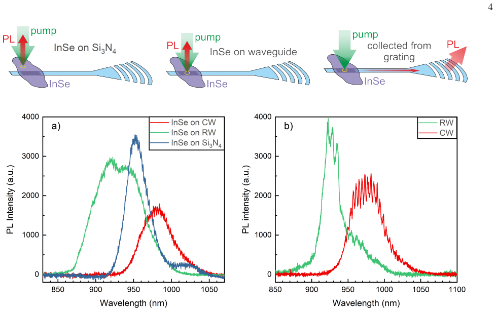
The authors show that a thin InSe flake placed on a Mie-resonant silicon nitride waveguide experiences Purcell-enhanced spontaneous emission. Time-resolved photoluminescence data indicate an excitonic decay time shortened by up to a factor of three relative to planar InSe. The extracted Purcell factors reach approximately 3 for out-of-plane excitons and 2.1 for in-plane excitons, directly confirming resonator-induced modification of the recombination rate.
What carries the argument
The Mie-resonant silicon nitride waveguide that spectrally overlaps the InSe photoluminescence band and enhances coupling of excitonic emission to the guided mode.
If this is right
- Resonator-induced control of excitonic recombination is achieved in layered InSe.
- vdW-dielectric interfaces function as a platform for integrated excitonic and quantum photonic devices.
- Spectral overlap between the Mie resonance and the InSe band produces Purcell factors of roughly 3 and 2.1 for the two exciton orientations.
- The hybrid geometry offers a scalable route to faster emission without etching or patterning the semiconductor itself.
Where Pith is reading between the lines
- The same waveguide approach could be applied to other van der Waals emitters to achieve comparable lifetime engineering.
- Tuning the resonance wavelength in situ might allow active control of the emission rate for single-photon sources.
- If non-radiative losses remain unchanged, the observed Purcell factor directly translates into higher quantum efficiency for on-chip devices.
Load-bearing premise
The measured reduction in decay time is produced by Purcell enhancement from the resonance and guided-mode coupling rather than by strain, interface defects, or altered non-radiative channels introduced during integration.
What would settle it
Fabricate an otherwise identical InSe-on-Si3N4 sample on a waveguide whose resonance is deliberately detuned from the InSe emission band and measure whether the decay time remains shortened; if the lifetime returns to the planar value, the resonance is required for the effect.
Figures


read the original abstract
Hybrid integration of layered van der Waals (vdW) semiconductors with dielectric resonant structures provides an effective approach for controlling excitonic emission dynamics. Here, we demonstrate Purcell-enhanced spontaneous emission from a thin InSe flake integrated with a Mie-resonant Si$_3$N$_4$ waveguide. The structure is designed to spectrally overlap with the InSe photoluminescence band and enhance coupling of excitonic emission to the guided mode. Time-resolved photoluminescence shows a reduction of the excitonic decay time by up to a factor of three relative to planar InSe. The extracted Purcell factors are approximately 3 for out-of-plane excitons and 2.1 for in-plane excitons. These results demonstrate resonator-induced control of excitonic recombination in layered InSe and highlight vdW-dielectric interfaces as a platform for integrated excitonic and quantum photonic devices.
Editorial analysis
A structured set of objections, weighed in public.
Referee Report
Summary. The manuscript demonstrates hybrid integration of a thin InSe flake with a Mie-resonant Si3N4 waveguide designed for spectral overlap with the InSe photoluminescence band. Time-resolved photoluminescence measurements report a reduction in excitonic decay time by up to a factor of three relative to planar InSe, from which Purcell factors of approximately 3 (out-of-plane excitons) and 2.1 (in-plane excitons) are extracted. The work positions vdW-dielectric interfaces as a platform for controlling excitonic recombination in integrated photonic devices.
Significance. If the lifetime reduction is confirmed to arise from radiative Purcell enhancement rather than non-radiative effects, the result would provide a concrete experimental demonstration of resonator-induced modification of excitonic dynamics in layered semiconductors, with potential relevance for quantum photonic integration. The numerical factors reported (factor-of-3 shortening, specific Purcell values) are falsifiable and could serve as benchmarks for future modeling of vdW-resonator coupling.
major comments (2)
- [Results and Discussion] The central interpretation—that the observed decay-time reduction directly yields Purcell factors of ~3 and ~2.1—requires that non-radiative recombination rates remain unchanged upon integration. The manuscript provides no control data on non-resonant planar Si3N4 substrates, absolute quantum-yield measurements, or intensity-dependent comparisons that would isolate the radiative component. This assumption is load-bearing for the extracted Purcell factors and the claim of Mie-resonance-induced enhancement.
- [Abstract and §3 (Experimental Results)] The abstract and main text state clear numerical outcomes (factor-of-3 reduction, Purcell factors 3 and 2.1) but supply no details on decay-curve fitting procedures, error bars, baseline subtraction, or how the in-plane versus out-of-plane contributions were separated. Without these, the quantitative extraction cannot be independently verified.
minor comments (2)
- [Throughout] Notation for the waveguide material alternates between Si3N4 and Si$_3$N$_4$; consistent use of the latter (or a defined abbreviation) would improve clarity.
- [Device Design] The manuscript would benefit from an explicit statement of the waveguide dimensions, resonance wavelength, and quality factor in the main text rather than (or in addition to) supplementary material.
Simulated Author's Rebuttal
We thank the referee for their careful and constructive review of our manuscript. The comments highlight important points regarding the interpretation of the lifetime reduction and the need for additional experimental details. We have revised the manuscript to address these concerns by adding control measurements, clarifying the data analysis procedures, and qualifying our claims where appropriate. Our point-by-point responses follow.
read point-by-point responses
-
Referee: [Results and Discussion] The central interpretation—that the observed decay-time reduction directly yields Purcell factors of ~3 and ~2.1—requires that non-radiative recombination rates remain unchanged upon integration. The manuscript provides no control data on non-resonant planar Si3N4 substrates, absolute quantum-yield measurements, or intensity-dependent comparisons that would isolate the radiative component. This assumption is load-bearing for the extracted Purcell factors and the claim of Mie-resonance-induced enhancement.
Authors: We agree that isolating the radiative contribution is essential for a robust interpretation. In the revised manuscript we have added time-resolved data for InSe flakes placed on planar (non-resonant) Si3N4 substrates fabricated under identical conditions; these control samples exhibit decay times statistically indistinguishable from the original planar InSe reference, indicating that the change in dielectric environment alone does not alter non-radiative rates appreciably. We have also included excitation-power-dependent measurements over the range used in the main experiment, confirming linear PL response and the absence of saturation or Auger effects that could modify non-radiative channels. Absolute quantum-yield measurements remain experimentally challenging in our micro-PL setup owing to uncertainties in collection efficiency; however, we have added a short discussion noting that any substrate-induced non-radiative changes would be comparable for resonant and non-resonant Si3N4 because both present similar dielectric constants and surface properties. The text now explicitly states that the reported Purcell factors are extracted under the assumption—now supported by the new controls—that non-radiative rates are unchanged, and we have softened the language accordingly. revision: partial
-
Referee: [Abstract and §3 (Experimental Results)] The abstract and main text state clear numerical outcomes (factor-of-3 reduction, Purcell factors 3 and 2.1) but supply no details on decay-curve fitting procedures, error bars, baseline subtraction, or how the in-plane versus out-of-plane contributions were separated. Without these, the quantitative extraction cannot be independently verified.
Authors: We appreciate the referee’s request for methodological transparency. The revised §3 now contains a dedicated subsection on data analysis that specifies: (i) the fitting model (single-exponential decay convolved with the measured instrument response function, with goodness-of-fit assessed via reduced χ² and residual inspection); (ii) background subtraction performed by averaging the pre-excitation signal over a 2 ns window; (iii) error bars obtained from the standard deviation across five independent spatial positions on each sample plus the covariance matrix of the fit parameters; and (iv) the separation of in-plane and out-of-plane exciton contributions, achieved via polarization-resolved detection aligned with the known dipole orientations of InSe excitons (out-of-plane dipoles dominate the A-exciton emission, while in-plane components are isolated by rotating the collection polarizer). These procedures are cross-referenced to the supplementary information, which includes representative raw decay curves, fit residuals, and polarization data. The abstract numbers remain unchanged but are now accompanied by the stated uncertainties (±0.3 for the factor-of-3 reduction and ±0.2/±0.1 for the two Purcell factors). revision: yes
Circularity Check
No circularity: experimental lifetime ratios extracted by standard definition
full rationale
The manuscript reports time-resolved photoluminescence measurements comparing excitonic decay times between InSe flakes integrated on Mie-resonant Si3N4 waveguides and planar reference samples. The Purcell factors (~3 for out-of-plane, ~2.1 for in-plane) are obtained directly from the observed lifetime reduction factor via the conventional relation F_p = τ_planar / τ_integrated under the assumption that non-radiative rates are unchanged. No equations, ansatzes, or derivations appear that reduce a claimed prediction to its own fitted inputs or to a self-citation chain; the result is a straightforward experimental ratio rather than a self-contained model. The interpretation that the shortening is radiative (Purcell) rather than non-radiative is an untested assumption but does not constitute circularity in the derivation sense.
Axiom & Free-Parameter Ledger
Reference graph
Works this paper leans on
-
[1]
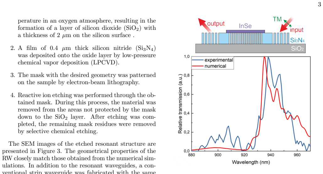
A silicon wafer was placed in a furnace at high tem- 3 perature in an oxygen atmosphere, resulting in the formation of a layer of silicon dioxide (SiO 2) with a thickness of 2µm on the silicon surface
-
[2]
A film of 0.4µm thick silicon nitride (Si 3N4) was deposited onto the oxide layer by low-pressure chemical vapor deposition (LPCVD)
-
[3]
The mask with the desired geometry was patterned on the sample by electron-beam lithography
-
[4]
Reactive ion etching was performed through the ob- tained mask. During this process, the material was removed from the areas not protected by the mask down to the SiO 2 layer. After etching was com- pleted, the remaining mask residues were removed by selective chemical etching. The SEM images of the etched resonant structure are presented in Figure 3. The...
-
[5]
N. P. Wilson, W. Yao, J. Shan, and X. Xu, Excitons and emergent quantum phenomena in stacked 2D semicon- ductors, Nature599, 383 (2021)
work page 2021
-
[6]
T. Mueller and E. Malic, Exciton physics and device ap- plication of two-dimensional transition metal dichalco- genide semiconductors, npj 2D Materials and Applica- tions2, 29 (2018)
work page 2018
-
[7]
A. G. Lamprianidis, X. Zambrana-Puyalto, C. Rock- stuhl, and I. Fernandez-Corbaton, Directional coupling of emitters into waveguides: A symmetry perspective, Laser & Photonics Reviews16, 2000516 (2022)
work page 2022
-
[8]
N. Verhart, G. Lepert, A. Billing, J. Hwang, and E. Hinds, Single dipole evanescently coupled to a mul- timode waveguide, Optics express22, 19633 (2014)
work page 2014
-
[9]
F. Peyskens, C. Chakraborty, M. Muneeb, D. Van Thourhout, and D. Englund, Integration of single photon emitters in 2d layered materials with a silicon nitride photonic chip, Nature communications 10, 4435 (2019)
work page 2019
-
[10]
T. Venanzi, H. Arora, S. Winnerl, A. Pashkin, P. Chava, A. Patan` e, Z. D. Kovalyuk, Z. R. Kudrynskyi, K. Watan- abe, T. Taniguchi, A. Erbe, M. Helm, and H. Schneider, Photoluminescence dynamics in few-layer InSe, Physical Review Materials 10.1103/PhysRevMaterials.4.044001 (2020)
-
[11]
B. R. Borodin, I. A. Eliseyev, A. I. Galimov, L. V. Kotova, M. V. Durnev, T. V. Shubina, M. A. Yagov- kina, and M. V. Rakhlin, Indirect-to-direct band-gap transition in few-layerβ-InSe as probed by photolu- minescence spectroscopy, Physical Review Materials8, 10.1103/PhysRevMaterials.8.014001 (2024)
-
[12]
D. V. Rybkovskiy, A. V. Osadchy, and E. D. Obraztsova, Transition from parabolic to ring-shaped valence band maximum in few-layer GaS, GaSe, and InSe, Physical Review B90, 10.1103/physrevb.90.235302 (2014)
-
[13]
M. Brotons-Gisbert, R. Proux, R. Picard, D. Andres- Penares, A. Branny, A. Molina-S´ anchez, J. F. S´ anchez- Royo, and B. D. Gerardot, Out-of-plane orientation of luminescent excitons in two-dimensional indium selenide, Nature Communications10, 1 (2019)
work page 2019
-
[14]
Y. C. Jun, R. M. Briggs, H. A. Atwater, and M. L. Brongersma, Broadband enhancement of light emission in silicon slot waveguides, Optics Express17, 7479 (2009)
work page 2009
-
[15]
L. Liebermeister, F. Petersen, A. v. M¨ unchow, D. Bur- chardt, J. Hermelbracht, T. Tashima, A. W. Schell, O. Benson, T. Meinhardt, A. Krueger,et al., Tapered fiber coupling of single photons emitted by a determinis- tically positioned single nitrogen vacancy center, Applied Physics Letters104(2014)
work page 2014
-
[16]
P. Tonndorf, O. Del Pozo-Zamudio, N. Gruhler, J. Kern, R. Schmidt, A. I. Dmitriev, A. P. Bakhtinov, A. I. Tar- takovskii, W. Pernice, S. Michaelis De Vasconcellos, and R. Bratschitsch, On-Chip Waveguide Coupling of a Lay- ered Semiconductor Single-Photon Source, Nano Letters 17, 5446 (2017)
work page 2017
-
[17]
C. Errando-Herranz, E. Sch¨ oll, R. Picard, M. Laini, S. Gyger, A. W. Elshaari, A. Branny, U. Wennberg, S. Barbat, T. Renaud, M. Sartison, M. Brotons-Gisbert, C. Bonato, B. D. Gerardot, V. Zwiller, and K. D. J¨ ons, Resonance Fluorescence from Waveguide-Coupled, Strain-Localized, Two-Dimensional Quantum Emitters, ACS Photonics8, 1069 (2021), 2002.07657
-
[18]
R. Wang, X. Jiang, S. Gao, J. Zhao, F. Zhang, W. Huang, T. Fan, W. Liang, Z. Li, H. Huang, Z. Guo, H. Wang, Y. Zhang, X. Zhang, Z. Luo, and H. Zhang, Unveiling the Stimulated Robust Carrier Lifetime of Surface-Bound Excitons and Their Photoresponse in InSe, Advanced Materials Interfaces6, 1 (2019)
work page 2019
-
[19]
S. R. Tamalampudi, Y.-Y. Lu, R. K. U, R. Sankar, C.- D. Liao, K. M. B, C.-H. Cheng, F. C. Chou, and Y.-T. Chen, High performance and bendable few-layered inse photodetectors with broad spectral response, Nano let- ters14, 2800 (2014)
work page 2014
-
[20]
A. E. Krasnok, A. E. Miroshnichenko, P. A. Belov, and Y. S. Kivshar, All-dielectric optical nanoantennas, Optics Express20, 20599 (2012)
work page 2012
-
[21]
D. V. Obydennov, D. A. Shilkin, D. N. Gulkin, E. V. Lyubin, D. M. Zhigunov, V. O. Bessonov, and A. A. Fedyanin, Asymmetric silicon dimers made by single-shot laser-induced transfer demultiplex light of different wave- lengths, Advanced Optical Materials12, 2302276 (2024)
work page 2024
-
[22]
J. F. Bauters, M. J. R. Heck, D. John, D. Dai, M.-C. Tien, J. S. Barton, A. Leinse, R. G. Heideman, D. J. Blu- menthal, and J. E. Bowers, Ultra-low-loss high-aspect- ratio Si3N4 waveguides, Optics Express19, 3163 (2011)
work page 2011
-
[23]
D. J. Blumenthal, R. Heideman, D. Geuzebroek, A. Leinse, and C. Roeloffzen, Silicon nitride in silicon photonics, Proceedings of the IEEE106, 2209 (2018)
work page 2018
-
[24]
M. Rakhlin, T. V. Antipov, A. D. Gartman, D. N. Gulkin, L. Kotova, A. Galimov, B. Borodin, I. Eliseyev, A. S. Shorokhov, and A. A. Fedyanin, Mie-resonant 7 silicon waveguide for efficient coupling with excitonic emitters in InSe, Journal of Materials Chemistry C 10.1039/d5tc03144c (2025)
- [25]
-
[26]
T. Bucher, A. Vaskin, R. Mupparapu, F. J. F. L¨ ochner, A. George, K. E. Chong, S. Fasold, C. Neumann, D.- Y. Choi, F. Eilenberger, F. Setzpfandt, Y. S. Kivshar, T. Pertsch, A. Turchanin, and I. Staude, Tailoring pho- toluminescence from MoS2 monolayers by Mie-resonant metasurfaces, ACS Photonics6, 1002 (2019)
work page 2019
-
[27]
C. Ma, X. Li, P. Huang, X. Liu, J. Yan, Z. Zheng, J. Yao, C. Du, Y. Liu, X. Li,et al., Enhanced optical absorption and emission from monolayer ws2 integrated onto a tio2 nanohole array, Advanced Optical Materials13, 2402015 (2025)
work page 2025
-
[28]
V. Bordo, Purcell factor for a cylindrical nanocavity: ab initio analytical approach, Journal of the Optical Society of America B29, 1799 (2012)
work page 2012
-
[29]
P. Androvitsaneas, A. B. Young, C. Schneider, S. Maier, M. Kamp, S. H¨ ofling, S. Knauer, E. Harbord, C. Y. Hu, J. G. Rarity, and R. Oulton, Charged quantum dot micropillar system for deterministic light-matter interac- tions, Phys. Rev. B93, 241409 (2016)
work page 2016
discussion (0)
Sign in with ORCID, Apple, or X to comment. Anyone can read and Pith papers without signing in.