Recognition: no theorem link
Emerging 2D Materials for Beyond von Neumann Computing: A Perspective
Pith reviewed 2026-05-12 04:06 UTC · model grok-4.3
The pith
The next decade of 2D materials progress will be decided by integrating graphene transistors, 2D memristors, and photonic structures on one semiconductor wafer.
A machine-rendered reading of the paper's core claim, the machinery that carries it, and where it could break.
Core claim
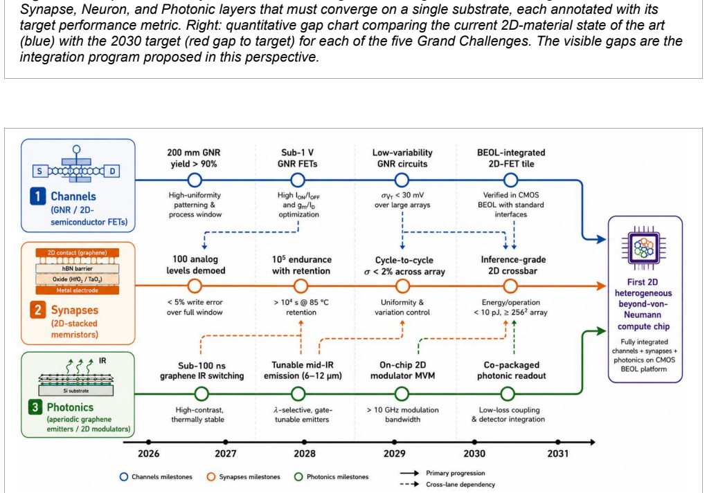
The paper states that after ten years of record single devices the decisive step is integration: graphene and graphene nanoribbon transistors as channel materials, oxide and 2D-integrated memristors for in-memory analog compute, and silicon-compatible 2D photonic and thermal-emitter structures, all placed on one semiconductor wafer. This unified platform would let devices compute where they store, process events rather than clock cycles, and shift workloads into the optical domain, directly addressing the end of Dennard scaling and the growing memory-processor gap.
What carries the argument
Wafer-scale integration of three device families—graphene transistors, 2D memristors, and 2D photonic structures—on a single silicon-compatible substrate, serving as the mechanism that turns separate device records into a beyond-von-Neumann system.
If this is right
- Graphene transistors can provide atomically thin, electrically tunable channels for logic beyond conventional silicon limits.
- 2D memristors enable in-memory analog computation that narrows the memory bandwidth gap.
- Photonic and thermal-emitter structures move selected workloads into the optical domain while remaining silicon compatible.
- Event-driven rather than clock-driven processing becomes practical once the three elements share a wafer.
- A single platform emerges for devices that both store and compute without constant data shuttling.
Where Pith is reading between the lines
- Successful integration would likely require new low-temperature transfer or growth methods to avoid damaging earlier layers.
- The same wafer approach could be tested first on smaller substrates to quantify yield before scaling to 300 mm.
- Even after integration, uniformity of 2D layers across large areas could still set the practical performance ceiling.
- Hybrid systems might combine the memristor array with photonic interconnects to reduce latency in data-heavy workloads.
Load-bearing premise
That combining the three device types on one wafer is technically feasible and will be the main factor that determines progress rather than yield, cost, or other limits.
What would settle it
Fabrication of a single wafer containing working graphene transistors, 2D memristors, and photonic elements that demonstrates measurable gains in bandwidth or energy over separately fabricated devices, or clear evidence that material or process incompatibility prevents such integration.
Figures


read the original abstract
The end of conventional Dennard scaling and the widening gap between memory bandwidth and arithmetic throughput have made the von Neumann partition a structural bottleneck rather than a transient one. Two-dimensional (2D) materials, with atomically thin geometries, electrically tunable carrier densities, and large optical responses, offer a unified platform on which to build devices that compute where they store, process events rather than clock cycles, and shift workload into the optical domain. This perspective surveys progress along three converging thrusts, graphene and graphene nanoribbon transistors as scalable channel materials, oxide and 2D-integrated memristors for in-memory analog compute, and silicon-compatible 2D photonic and thermal-emitter structures for optical computing primitives. Our central argument is that the 2D-materials community has spent a decade producing record devices, and the next decade will be decided by who first integrates three of them on a single semiconductor wafer.
Editorial analysis
A structured set of objections, weighed in public.
Referee Report
Summary. This perspective surveys progress in three thrusts of 2D materials for beyond-von-Neumann computing: graphene and graphene-nanoribbon transistors as channel materials, oxide and 2D-integrated memristors for in-memory analog computation, and silicon-compatible 2D photonic/thermal-emitter structures. The central claim, stated in the abstract, is that a decade of record individual devices has been achieved and that the next decade will be decided by the first successful integration of all three device types on a single semiconductor wafer.
Significance. As a high-level synthesis of prior device demonstrations rather than new data or derivations, the manuscript usefully consolidates literature across electronic, memristive, and photonic 2D platforms and identifies integration as the key remaining bottleneck. If the thesis holds, it could usefully redirect community effort toward monolithic, wafer-scale co-integration challenges. The survey format itself is a strength in providing a unified narrative across disparate device records.
major comments (2)
- Abstract (central argument): the claim that 'the next decade will be decided by who first integrates three of them on a single semiconductor wafer' is presented as the load-bearing thesis but is unsupported by any analysis of integration feasibility, thermal/lattice compatibility constraints, or comparison against other potential bottlenecks such as yield, uniformity, or fundamental physics limits. This renders the decisive-factor assertion speculative rather than substantiated.
- Introduction / survey sections on the three thrusts: while individual device records are cited, the manuscript does not quantify or reference any existing attempts at co-integration of graphene transistors with 2D memristors and photonic elements, leaving the feasibility premise untested within the paper's own scope.
minor comments (3)
- Clarify whether 'three of them' refers to one device from each thrust or any combination; the current wording in the abstract is ambiguous.
- Add a short table or timeline summarizing key device metrics (on/off ratio, switching energy, etc.) across the three thrusts to improve readability of the survey.
- Ensure all cited works include DOIs or arXiv identifiers for the benefit of readers.
Simulated Author's Rebuttal
We thank the referee for the constructive comments on our perspective manuscript. We agree that the central thesis requires clearer framing as a forward-looking hypothesis and that the discussion of integration should be expanded to better reflect the current literature. We will revise accordingly while preserving the survey's scope.
read point-by-point responses
-
Referee: Abstract (central argument): the claim that 'the next decade will be decided by who first integrates three of them on a single semiconductor wafer' is presented as the load-bearing thesis but is unsupported by any analysis of integration feasibility, thermal/lattice compatibility constraints, or comparison against other potential bottlenecks such as yield, uniformity, or fundamental physics limits. This renders the decisive-factor assertion speculative rather than substantiated.
Authors: As a perspective article, the statement is intended as a synthesis of device records and a directional hypothesis rather than a quantitative prediction. We acknowledge the need for additional context and will revise the abstract to present integration as a central open challenge rather than the sole decisive factor. We will also add a concise paragraph in the introduction summarizing known thermal, lattice, and process compatibility issues from the 2D materials literature, while explicitly noting that a full comparative analysis of all bottlenecks lies outside the scope of this survey. revision: yes
-
Referee: Introduction / survey sections on the three thrusts: while individual device records are cited, the manuscript does not quantify or reference any existing attempts at co-integration of graphene transistors with 2D memristors and photonic elements, leaving the feasibility premise untested within the paper's own scope.
Authors: The manuscript focuses on individual device milestones to establish the progress achieved so far. To address the point, we will insert a dedicated paragraph in the introduction that reviews the limited existing literature on co-integration attempts (including any hybrid or preliminary demonstrations) and notes their scarcity. This addition will explicitly connect the absence of mature co-integration examples to the argument that wafer-scale integration of the three device classes remains the key next step. revision: yes
Circularity Check
No significant circularity in perspective survey
full rationale
This manuscript is explicitly a perspective article that synthesizes prior device demonstrations across three thrusts without introducing new equations, derivations, fitted parameters, or quantitative models. The central claim—that future progress hinges on wafer-scale integration of graphene transistors, 2D memristors, and silicon-compatible photonics—is presented as a forward-looking opinion rather than a deductive result. No load-bearing steps reduce by construction to self-citations, ansatzes, or renamed empirical patterns; the argument remains self-contained as a high-level survey of external literature.
Axiom & Free-Parameter Ledger
axioms (1)
- domain assumption 2D materials can be combined with silicon processing to achieve functional integration of transistors, memristors, and photonic elements.
Reference graph
Works this paper leans on
-
[1]
The chips are down for Moore's law,
M. M. Waldrop, "The chips are down for Moore's law," Nature News, vol. 530, no. 7589, pp. 144 to 147, 2016
work page 2016
-
[2]
Memristor: The missing circuit element,
L. O. Chua, "Memristor: The missing circuit element," IEEE Trans. Circuit Theory, vol. 18, no. 5, pp. 507 to 519, 1971
work page 1971
-
[3]
D. B. Strukov, G. S. Snider, D. R. Stewart, and R. S. Williams, "The missing memristor found," Nature, vol. 453, pp. 80-83, 2008
work page 2008
-
[4]
Neuromorphic electronic systems,
C. Mead, "Neuromorphic electronic systems," Proc. IEEE, vol. 78, no. 10, pp. 1629 to 1636, 1990
work page 1990
-
[5]
Beyond CMOS computing with spin and polarization,
S. Manipatruni, D. E. Nikonov, and I. A. Young, "Beyond CMOS computing with spin and polarization," Nature Physics, vol. 14, pp. 338 to 343, 2018
work page 2018
-
[6]
Deep learning with coherent nanophotonic circuits,
Y. Shen et al., "Deep learning with coherent nanophotonic circuits," Nature Photonics, vol. 11, pp. 441 to 446, 2017
work page 2017
-
[7]
Parallel convolutional processing using an integrated photonic tensor core,
J. Feldmann et al., "Parallel convolutional processing using an integrated photonic tensor core," Nature, vol. 589, pp. 52 to 58, 2021
work page 2021
-
[8]
Electric field effect in atomically thin carbon films,
K. S. Novoselov et al., "Electric field effect in atomically thin carbon films," Science, vol. 306, no. 5696, pp. 666 to 669, 2004
work page 2004
-
[9]
Y. Banadaki and S. Sharifi, Graphene Nanostructures: Modeling, Simulation, and Applications in Electronics and Photonics. Jenny Stanford Publishing
-
[10]
Y. M. M. Banadaki, "Physical modeling of graphene nanoribbon field effect transistor using non-equilibrium Green function approach for integrated circuit design," Ph.D. dissertation, Louisiana State University and Agricultural & Mechanical College, 2016
work page 2016
-
[11]
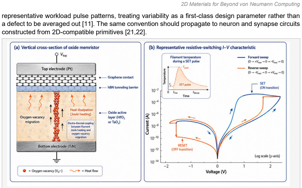
A. Gooran-Shoorakchaly, S. Sharif, and Y. Banad, "Investigating the effect of electrical and thermal transport properties on oxide-based memristors performance and reliability," Sci. Rep., vol. 15, no. 1, art. 18646, 2025
work page 2025
-
[12]
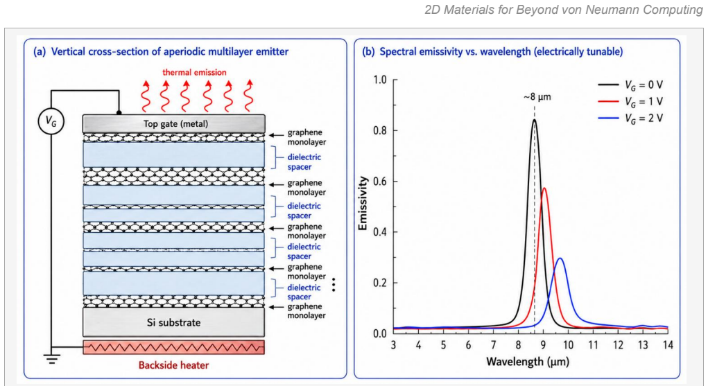
S. Sharifi, Y. M. Banadaki, V. F. Nezhad, G. Veronis, and J. P. Dowling, "Aperiodic multilayer graphene based tunable and switchable thermal emitter at mid-infrared frequencies," J. Appl. Phys., vol. 124, no. 23, 2018
work page 2018
-
[13]
S. Sharifi, "Aperiodic multilayer graphene-based tunable and switchable thermal emitter at mid-infrared frequencies," M.S. thesis, Louisiana State University, 2018
work page 2018
-
[14]
Photonics and optoelectronics of 2D semiconductor transition metal dichalcogenides,
K. F. Mak and J. Shan, "Photonics and optoelectronics of 2D semiconductor transition metal dichalcogenides," Nature Photonics, vol. 10, pp. 216 to 226, 2016
work page 2016
-
[15]
Graphene and two-dimensional materials for silicon technology,
D. Akinwande et al., "Graphene and two-dimensional materials for silicon technology," Nature, vol. 573, pp. 507 to 518, 2019
work page 2019
-
[16]
Uniform nucleation and epitaxy of bilayer molybdenum disulfide on sapphire,
L. Liu et al., "Uniform nucleation and epitaxy of bilayer molybdenum disulfide on sapphire," Nature, vol. 605, pp. 69 to 75, 2022
work page 2022
-
[17]
A novel graphene nanoribbon field effect transistor for integrated circuit design,
Y. M. Banadaki and A. Srivastava, "A novel graphene nanoribbon field effect transistor for integrated circuit design," in Proc. IEEE 56th Int. Midwest Symp. Circuits and Systems (MWSCAS), 2013
work page 2013
-
[18]
Effect of edge roughness on static characteristics of graphene nanoribbon field effect transistor,
Y. M. Banadaki and A. Srivastava, "Effect of edge roughness on static characteristics of graphene nanoribbon field effect transistor," Electronics, vol. 5, no. 1, art. 11, 2016
work page 2016
-
[19]
Dielectrics for graphene transistors for emerging integrated circuits,
A. Srivastava, Y. M. Banadaki, and M. S. Fahad, "Dielectrics for graphene transistors for emerging integrated circuits," ECS Trans., vol. 61, no. 2, pp. 351 to 361, 2014
work page 2014
-
[20]
Graphene nanoribbon field effect transistor for nanometer-size on-chip temperature sensor,
Y. M. Banadaki, A. Srivastava, and S. Sharifi, "Graphene nanoribbon field effect transistor for nanometer-size on-chip temperature sensor," in Nanosensors, Biosensors, and Info-Tech Sensors and Systems, Proc. SPIE, vol. 9802, pp. 12 to 20, 2016
work page 2016
-
[21]
R. Siddique, M. Eftimie, and Y. Banad, "A comparative analysis of neuromorphic neuron circuits for enhanced power efficiency and spiking frequency in 22 nm CMOS technology," in Proc. IEEE 67th Int. Midwest Symp. Circuits and Systems (MWSCAS), 2024
work page 2024
-
[22]
S. M. J. Motaman, S. S. Sharifi, and Y. Banad, "Enhancing neuromorphic computing: A high-speed, low-power integrate- and-fire neuron circuit utilizing nanoscale side-contacted field-effect diode technology," in IEEE Int. Midwest Symp. Circuits and Systems (MWSCAS), 2013
work page 2013
-
[23]
Memory devices and applications for in-memory computing,
A. Sebastian, M. Le Gallo, R. Khaddam-Aljameh, and E. Eleftheriou, "Memory devices and applications for in-memory computing," Nature Nanotechnology, vol. 15, pp. 529 to 544, 2020
work page 2020
-
[24]
T. Mikolajick, S. Slesazeck, M. H. Park, and U. Schroeder, "Ferroelectric hafnium oxide for ferroelectric random-access memories and ferroelectric field-effect transistors," MRS Bulletin, vol. 43, pp. 340 to 346, 2018
work page 2018
-
[25]
Magnetoresistive random access memory,
D. Apalkov, B. Dieny, and J. M. Slaughter, "Magnetoresistive random access memory," Proc. IEEE, vol. 104, no. 10, pp. 1796 to 1830, 2016
work page 2016
-
[26]
Accurate deep neural network inference using computational phase-change memory,
V. Joshi et al., "Accurate deep neural network inference using computational phase-change memory," Nature Communications, vol. 11, art. 2473, 2020
work page 2020
-
[27]
Equivalent-accuracy accelerated neural-network training using analogue memory,
S. Ambrogio et al., "Equivalent-accuracy accelerated neural-network training using analogue memory," Nature, vol. 558, pp. 60 to 67, 2018
work page 2018
discussion (0)
Sign in with ORCID, Apple, or X to comment. Anyone can read and Pith papers without signing in.