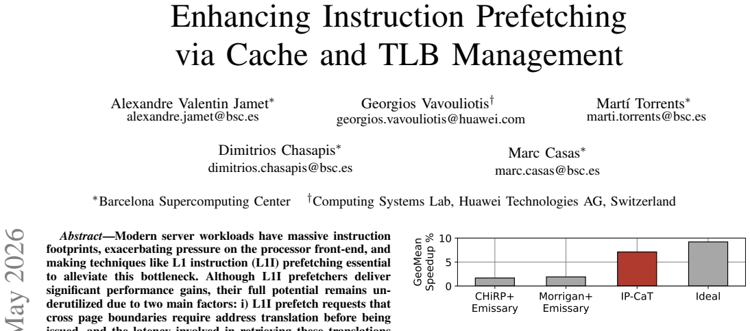
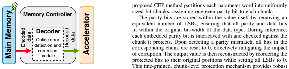
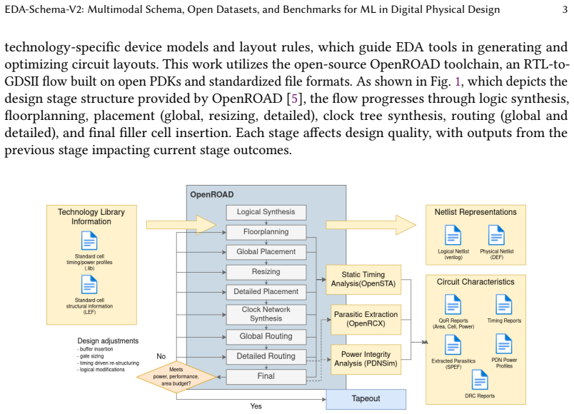
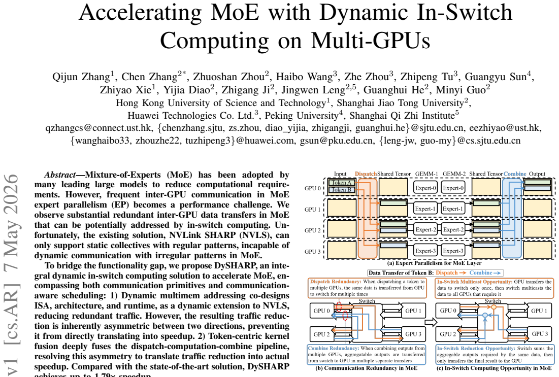
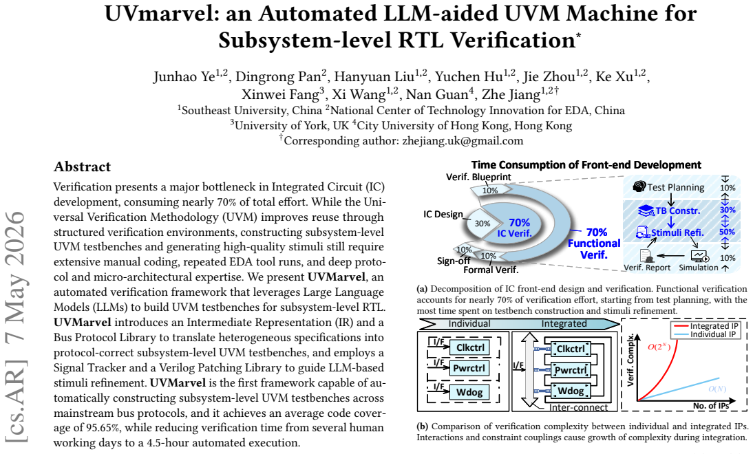
pith. machine review for the scientific record. sign in

cs.AR

Hardware Architecture

Covers systems organization and hardware architecture. Roughly includes material in ACM Subject Classes C.0, C.1, and C.5.

0
cs.AR 2026-05-14 Recognition

PoisonCap gives CHERI strict use-after-free at zero overhead

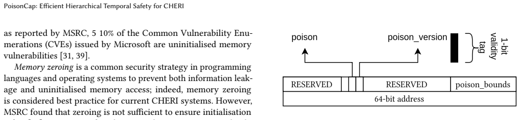
PoisonCap: Efficient Hierarchical Temporal Safety for CHERI

Poison capability format replaces shadow bitmaps, auto-zeros on reuse, and supports hierarchical delegation.

Figure from the paper full image
abstract click to expand
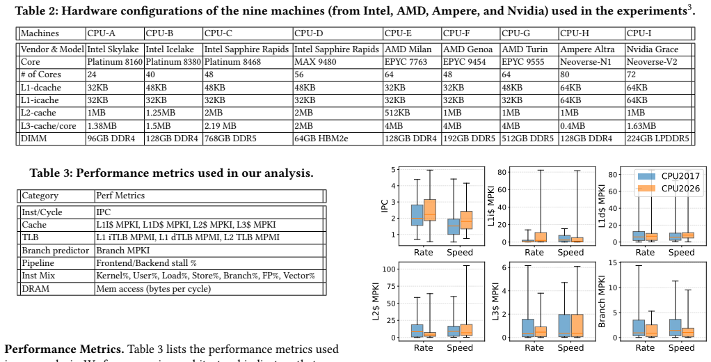
In this paper, we present PoisonCap: scalable temporal safety with strict use-after-free protection and initialisation safety for CHERI systems. Efficient memory safety is an increasing priority for programming languages, operating systems, and hardware designs, and CHERI is a leading hardware/software system that provides native spatial safety and a foundation for temporal memory safety. Cornucopia Reloaded, the current state-of-the-art CHERI temporal safety solution, provides use-after-reallocation safety instead of stronger use-after-free safety, and is not able to enforce initialisation safety. We show that a new 'poison' capability format can be used to enforce strict use-after-free and initialisation safety, and also to communicate memory state to the microarchitecture for efficient cache management of quarantined memory. We enable elegant delegation of memory poisoning privilege using capability bounds to allow nested allocators to enforce safety on their consumers without disturbing upstream allocators. PoisonCap can replace the Cornucopia shadow bitmap, and also automatically zeros memory on reallocation, or optionally traps on read-before-write to enforce initialisation safety. As a result, it incurs no fundamental overhead relative to a Cornucopia baseline that zeros before reallocation, strengthening CHERI temporal safety without performance overhead.
0
0
cs.AR 2026-05-13 2 theorems

Joint TLB-cache tweaks boost instruction prefetching 8.7%

Enhancing Instruction Prefetching via Cache and TLB Management

Small translation buffer and trimodal replacement policy cut delays and evict unused code lines in large-footprint server workloads.

Figure from the paper full image
abstract click to expand
Modern server workloads exhibit massive instruction footprints that heavily pressure the processor front-end, making L1 instruction (L1I) prefetching critical for sustaining performance. However, this paper shows that current L1I prefetchers fail to reach their full potential due to two key limitations. First, L1I prefetches crossing page boundaries require address translation before issuance, and translation latency reduces prefetch timeliness. Second, the reuse behavior of code lines fetched by L1I prefetches is highly heterogeneous: while some lines are reused many times, others are dead-on-arrival. This paper introduces Instruction Prefetch-Centric Cache and TLB Management (IP-CaT), the first microarchitectural framework jointly optimizing TLB and cache management for L1I prefetching. IP-CaT consists of two components: (i) the translation Prefetch Buffer (tPB), a small structure colocated with the second-level TLB (sTLB) that stores page table entries fetched by page-crossing L1I prefetches, reducing translation overheads; and (ii) the Trimodal Instruction Prefetch Replacement Policy (TIPRP), a decision-tree-based L2 cache replacement policy specialized for lines fetched by L1I prefetches. We evaluate IP-CaT with three state-of-the-art L1I prefetchers: EPI, FNL+MMA, and Barca. Across 105 contemporary server workloads, IP-CaT consistently improves performance. For example, IP-CaT+EPI achieves an 8.7% geomean speedup over EPI alone. We further show that IP-CaT outperforms state-of-the-art instruction TLB prefetching, advanced TLB replacement (CHiRP), and state-of-the-art code-aware, prefetch-aware, and general-purpose cache replacement policies, including Emissary, SHiP++, and Mockingjay.
0
0
cs.AR 2026-05-13 Recognition

FPGA SoC matches silicon SNN accuracy for neuromorphic edge tasks

Heterogeneous SoC Integrating an Open-Source Recurrent SNN Accelerator for Neuromorphic Edge Computing on FPGA

Heterogeneous integration of open-source ReckOn accelerator with RISC-V and ARM enables validation and online learning on Braille data.

Figure from the paper full image
abstract click to expand
The growing popularity of Spiking Neural Networks (SNNs) and their applications has led to a significant fast-paced increase of neuromorphic architectures capable of mimicking the spike-based data processing typical of biological neurons. The efficient power consumption and parallel computing capabilities of the SNNs lead researchers towards the development of digital accelerators, which exploit such features to bring fast and low-power computation on edge devices. The spread of digital neuromorphic hardware however is slowed down by the prohibitive costs that the silicon tape out of circuits brings, that's why targeting Field Programmable Gate Arrays (FPGAs) could represent a viable alternative, offering a flexible and cost-effective platform for implementing digital neuromorphic systems and helping the spread of open-source hardware designs. In this work we present an heterogeneous System-on-Chip (SoC) where the operations of ReckOn, a Recurrent SNN accelerator, are managed through the integration with traditional processors. These include the RISC-V-based, open-source microcontroller X-HEEP and the ARM processor featured in Zynq Ultrascale systems. We validate our design by reproducing the classification results through the implementation on FPGA of the taped-out version of ReckOn in order to check the equivalence of the accuracy and the characteristics in terms of physical implementation. In a second set of experiments, we evaluate the online learning capability of the solution in classifying a subset of the Braille digit dataset recently used to compare neuromorphic frameworks and platforms.
0
0
cs.AR 2026-05-12 2 theorems

Dynamic scheduler lifts MoE inference 1.3-1.6x on PIM hardware

Sieve: Dynamic Expert-Aware PIM Acceleration for Evolving Mixture-of-Experts Models

Runtime token-distribution decisions reduce imbalance for modern models that activate few experts unevenly.

Figure from the paper full image
abstract click to expand
Mixture-of-Experts (MoE) has become a dominant architecture for scaling large language models (LLMs). However, the execution characteristics of MoE inference are changing rapidly and increasingly mismatch the assumptions underlying existing Processing-in-Memory (PIM) systems. Prior PIM systems for LLMs rely on static rules to offload memory-bound operations to PIM, without accounting for the combined effects of load imbalance and inter-GPU communication. Meanwhile, modern MoE models activate fewer experts out of increasingly many, creating a bimodal expert distribution: a small set of experts receives many tokens, while a long tail of experts receives only one or a few. We identify a trend in modern MoE models toward increasingly bimodal token-to-expert distributions, quantify the resulting disparity in arithmetic intensity across experts, and show that this disparity dramatically reduces the efficiency of state-of-the-art PIM systems for LLMs. To address this problem, we propose a scheduler for serving MoE models on multi-GPU systems with attached HBM-PIM stacks. Our scheduler partitions expert execution between GPU and PIM based on runtime token-to-expert distributions, while jointly considering interconnect overhead, memory bandwidth, GPU throughput, and PIM throughput. Moreover, we propose Sieve, a runtime framework that employs the scheduler to coordinate execution across GPUs and their attached HBM-PIM stacks. Sieve overlaps GPU computation, PIM computation, and intra- and inter-device communication while preserving cross-device dependencies induced by expert parallelism. Sieve is evaluated on our cycle-accurate simulator based on Ramulator 2.0. Compared to state-of-the-art PIM systems for MoE, Sieve improves both throughput and interactivity by 1.3x, 1.3x, and 1.6x on Qwen3.5-397B-A17B, GPT-OSS-120B, and Qwen3-30B-A3B, respectively.
0
0
cs.AR 2026-05-12 Recognition

TLX adds MIMW warp-group control to Triton for modern GPUs

TLX: Hardware-Native, Evolvable MIMW GPU Compiler for Large-scale Production Environments

Preserves blocked programming while enabling customization for async hardware and cluster features in production systems.

Figure from the paper full image
abstract click to expand
Modern GPUs increasingly rely on specialized hardware units and asynchronous coordination mechanisms, so performance depends on orchestrating data movement, tensor-core computation, and synchronization rather than exposing more thread-level parallelism. This creates a programming-model tension: if too much execution structure is hidden, the compiler must catch up to new hardware mechanisms; if too much is exposed, the burden of orchestration falls back onto the programmer. We present TLX (Triton Low-level Language Extensions), built around MIMW (Multi-Instruction, Multi-Warp), which expresses orchestration at warp-group granularity while preserving Triton's productive blocked programming model for regular computation. TLX realizes this idea as an embedded extension to Triton, exposing explicit interfaces for multi-warp execution, local-memory orchestration, asynchronous operations, and cluster-aware control. Our evaluation shows that TLX supports substantial customization with limited development effort while remaining competitive with state-of-the-art implementations. TLX-authored kernels have been deployed in large-scale training and inference production systems. Our code is open sourced at https://github.com/facebookexperimental/triton.
0
0
cs.AR 2026-05-12 Recognition

Hybrid chip runs GNN at 2.94M events/sec for physics triggers

Reconfigurable Computing Challenge: Real-Time Graph Neural Networks for Online Event Selection in Big Science

FPGA plus AI Engine tiles deliver 53 percent higher throughput than pure FPGA while using only 19 percent DSP resources for Belle II event s

Figure from the paper full image
abstract click to expand
Graph neural networks are increasingly adopted in trigger systems for collider experiments, where strict latency and throughput constraints render deployment on embedded platforms challenging. As detectors move towards higher granularity, the number of inputs per inference increase and FPGA-only solutions face resource bottlenecks. This work presents an end-to-end demonstrator for the real-time deployment of a dynamic Graph Neural Network for the Belle II electromagnetic calorimeter hardware trigger on the AMD Versal VCK190, leveraging both FPGA fabric and AI Engine tiles. We develop a Python-based semi-automated design flow covering operator fusion, partitioning, mapping, spatial parallelization, and kernel-level optimization. Our design achieves a throughput of 2.94 million events per second at an end-to-end latency of 7.15 microseconds. Compared to the FPGA-only baseline, this represents a 53% throughput improvement while reducing DSP utilization from 99% to 19% at 29% AI Engine tile utilization. To validate the deployment, an interactive visualization pipeline enables real-time monitoring of inference results on the physical demonstrator.
0
0
cs.AR 2026-05-12 2 theorems

Error profiles detect stolen approximate circuit IP despite mimicry

ObfAx: Obfuscation and IP Piracy Detection in Approximate Circuits

A comparison method spots pirated approximate hardware even when attackers adjust function to match error rates and hardware costs.

Figure from the paper full image
abstract click to expand
Approximate circuits often achieve exceptional trade-offs between computational accuracy and hardware efficiency, making them attractive for deployment as reusable Intellectual Property (IP) cores. However, safeguarding such circuits against piracy is critical for enabling sustainable commercialization of approximate computing. This work addresses the emerging challenge of IP protection and piracy detection in the context of approximate hardware. We introduce a novel adversarial threat model, approximate obfuscation, in which an attacker not only conceals the design through structural obfuscation but also introduces functional modifications to ensure that the resulting circuit exhibits nearly identical error characteristics and hardware metrics as the original IP. To counter this threat, we propose an automated framework that extracts and compares statistical error profiles of protected IP cores and suspicious circuits, enabling systematic detection of potential IP theft. Through extensive experiments on a diverse set of approximate multipliers, we analyze the resilience of different approximate multipliers against approximate obfuscation. Our results provide new insights into the interplay between obfuscation, approximation, and IP protection.
0
0
cs.AR 2026-05-12 2 theorems

Piezoelectric sensors turn desk vibrations into six-gesture commands

Towards an End-To-End System for Real-Time Gesture Recognition from Surface Vibrations

End-to-end pipeline with 8722-parameter CNN reaches high accuracy even on unseen users

Figure from the paper full image
abstract click to expand
Sensing surface vibrations promise unobtrusive interaction for smart home systems by enabling gesture recognition on existing everyday surfaces without disturbing living-space design. Existing approaches typically address only parts of the processing chain, such as sensing hardware or offline gesture recognition, rather than providing an end-to-end system from surface-mounted sensors to the evaluation of the prediction model. This paper presents a custom sensor system and a configurable data-to-model pipeline for gesture recognition on a standard office desk. Our hardware enables a low-noise sensing of the vibrations using piezoelectric sensors. Building on a modular signal-processing framework, we model the full chain from continuous recordings through variable pre-processing to a model-ready dataset, and process the resulting data with compact depthwise separable 1D-CNNs. We conduct a joint search over pre-processing and model hyperparameters and identify a configuration with 8,722 parameters that uses band-pass filtering, fixed-length windows, and min-max normalization. On a self-recorded dataset with 15 participants performing six gestures this configuration achieves high accuracies across different data splitting methods, including strong user-independent performance in a leave-one-subject-out cross-validation.
0
0
cs.AR 2026-05-12 2 theorems

LLM agents size RF amplifiers via resource allocation

RFAmpDesigner: A Self-Evolving Multi-Agent LLM Framework for Automated Radio Frequency Amplifier Design

The framework converts parameter tuning to resource distribution and reuses past designs to reach 10-50 GHz targets without heavy fine-tuned

Figure from the paper full image
abstract click to expand
Automating radio frequency (RF) amplifier design remains challenging because existing methods suffer from the curse of dimensionality, weak use of domain knowledge, and poor transferability, leading to low data efficiency. Meanwhile, although large language models (LLMs) have shown promise in many scientific domains, applying them directly to RF sizing is nontrivial due to the numerical nature of circuit optimization and the reliance on domain-specific design flows. To address this, this paper proposes RFAmpDesigner, a multi-agent framework that automates RF amplifier sizing. It introduces a resource-allocation middleware that reframes high-dimensional parameter tuning as a low-dimensional resource distribution problem, making it easier to inject sizing knowledge into general-purpose LLMs. The framework also follows standard design practice, enabling LLMs to distinguish between high- and low-cost actions and search in parallel. To realize a self-evolving optimization process, the framework employs retrieval-augmented generation (RAG) to reuse past knowledge and experience from memory base. As a proof of concept, we apply RFAmpDesigner to low noise amplifiers of varying complexity. The experimental results show that it can automatically synthesize designs with fractional bandwidths ranging from 10\% to 80\% and center frequencies from 10 GHz to 50 GHz. To the best of our knowledge, this work develops the first LLM-driven approach for RF amplifier sizing that operates on design concepts instead of treating netlists as text, offering a novel solution to mitigate data scarcity in RF design.
0
0
cs.AR 2026-05-11 3 theorems

KV-cache movement regularization cuts static-graph LLM latency spikes

KV-RM: Regularizing KV-Cache Movement for Static-Graph LLM Serving

Variable-length requests no longer force over-reservation when transfers are coalesced beneath the fixed decoder.

Figure from the paper full image
abstract click to expand
Static-graph LLM decoders provide predictable launches, fixed tensor shapes, and low submission overhead, but online decoding exposes highly irregular KV-cache behavior: request lengths differ, EOS events arrive asynchronously, and logical histories fragment over time. Dynamic runtimes recover flexibility through paged KV management and step-level scheduling, while static-graph executors often over-reserve memory and suffer burst-time latency outliers. This paper studies whether much of this variability can be absorbed below a fixed decode interface. We present KV-RM, a runtime design that regularizes KV-cache movement beneath a static-graph LLM decoder. KV-RM decouples logical KV histories from physical storage, tracks active KV state through a block pager, and materializes each decode step through a single committed descriptor. A merge-staged transport path coalesces non-contiguous KV mappings into a small number of large transfer groups before a fixed-shape attention kernel consumes them. Optional bounded far-history summaries can be enabled under the same interface, but the core design does not depend on them. On a 2-GPU NVIDIA A100 node, KV-RM improves mixed-length decoding throughput and tail latency relative to a static-graph baseline, reduces reserved KV memory across workload families, and removes severe burst-time latency spikes under production-trace replay. These results suggest that KV-cache movement, rather than kernel shape, can be an effective boundary for recovering runtime flexibility in static-graph LLM serving.
0
0
cs.AR 2026-05-11 Recognition

Wafer integration of three 2D devices decides next computing decade

Emerging 2D Materials for Beyond von Neumann Computing: A Perspective

Graphene transistors, memristors, and photonic structures must share one silicon wafer to close the memory-processor gap.

Figure from the paper full image
abstract click to expand
The end of conventional Dennard scaling and the widening gap between memory bandwidth and arithmetic throughput have made the von Neumann partition a structural bottleneck rather than a transient one. Two-dimensional (2D) materials, with atomically thin geometries, electrically tunable carrier densities, and large optical responses, offer a unified platform on which to build devices that compute where they store, process events rather than clock cycles, and shift workload into the optical domain. This perspective surveys progress along three converging thrusts, graphene and graphene nanoribbon transistors as scalable channel materials, oxide and 2D-integrated memristors for in-memory analog compute, and silicon-compatible 2D photonic and thermal-emitter structures for optical computing primitives. Our central argument is that the 2D-materials community has spent a decade producing record devices, and the next decade will be decided by who first integrates three of them on a single semiconductor wafer.
0
0
cs.AR 2026-05-11 Recognition

ReRAM-on-logic chip reaches 14-136 tokens per second on LLMs

31.1 A 14.08-to-135.69Token/s ReRAM-on-Logic Stacked Outlier-Free Large-Language-Model Accelerator with Block-Clustered Weight-Compression and Adaptive Parallel-Speculative-Decoding

Outlier-free quantization and parallel speculative decoding yield 4.5-7x speedup over standard methods in a 55nm stacked design.

Figure from the paper full image
abstract click to expand
This work presents a 55nm speculative decoding-based LLM accelerator with bumping-based face-to-face ReRAM-on-logic stacking technology. It features a local rotation unit for outlier-free low-bit quantization, a stacking-aware PNM architecture co-designed with blockwise vector quantization to reduce weight EMA overheads, and an adaptive parallel speculative decoding scheme with an out-of-order scheduler for high resource and bandwidth utilization. Our chip achieves 14.08-to-135.69token/s and 4.46-to-7.17x speedup over vanilla speculative decoding.
0
0
cs.AR 2026-05-11 2 theorems

New cache bypass method meets deadlines while boosting heterogeneous system speed

HyDRA: Deadline and Reuse-Aware Cacheability for Hardware Accelerators

LERN clustering predicts accelerator reuse at the shared cache to guide HyDRA decisions that cut misses and raise throughput across variedSo

Figure from the paper full image
abstract click to expand
The system-level cache is a critical resource shared by processor cores and domain-specific accelerators in heterogeneous systems on chips (SoCs). The strict QoS requirements of accelerators, such as deadlines, can lead to severe performance degradation of processor cores. Thus, managing the shared cache efficiently between cores and accelerators becomes crucial. State-of-the-art cache management techniques perform reuse-aware bypassing of accesses from cores with the help of reuse predictors to improve performance. However, architectural differences between accelerators and processor cores (often associated with deep cache hierarchies) can lead to significantly different reuse patterns at the shared cache. We propose a novel clustering-based methodology, LERN, for learning and predicting the reuse behavior of hardware accelerators at the shared cache. We then propose a deadline and reuse-aware cache management strategy, HyDRA, which explores a novel tradeoff between reuse and deadline awareness for performance efficiency. It uses LERN to dynamically predict the reuse behavior of the accelerator accesses and make bypass decisions to maximize the system throughput while meeting accelerator deadlines. We evaluate HyDRA across different workloads and varied accelerator configurations. It significantly improves the system performance and reduces the accelerator deadline miss rate.
0
0
cs.AR 2026-05-11 2 theorems

HyDRA balances accelerator deadlines with cache reuse via clustering

HyDRA: Deadline and Reuse-Aware Cacheability for Hardware Accelerators

A predictor learns accelerator access patterns at the shared cache and decides bypasses to raise throughput while cutting deadline misses.

Figure from the paper full image
abstract click to expand
The system-level cache is a critical resource shared by processor cores and domain-specific accelerators in heterogeneous systems on chips (SoCs). The strict QoS requirements of accelerators, such as deadlines, can lead to severe performance degradation of processor cores. Thus, managing the shared cache efficiently between cores and accelerators becomes crucial. State-of-the-art cache management techniques perform reuse-aware bypassing of accesses from cores with the help of reuse predictors to improve performance. However, architectural differences between accelerators and processor cores (often associated with deep cache hierarchies) can lead to significantly different reuse patterns at the shared cache. We propose a novel clustering-based methodology, LERN, for learning and predicting the reuse behavior of hardware accelerators at the shared cache. We then propose a deadline and reuse-aware cache management strategy, HyDRA, which explores a novel tradeoff between reuse and deadline awareness for performance efficiency. It uses LERN to dynamically predict the reuse behavior of the accelerator accesses and make bypass decisions to maximize the system throughput while meeting accelerator deadlines. We evaluate HyDRA across different workloads and varied accelerator configurations. It significantly improves the system performance and reduces the accelerator deadline miss rate.
0
0
cs.AR 2026-05-11 2 theorems

Reconfigurable multiplier cuts power 44-68% in RISC-V core

A Reconfigurable Multiplier Architecture for Error-Resilient Applications in RISC-V Core

A mulscr register lets the processor switch accuracy levels at runtime, saving energy on error-tolerant tasks like matrix multiplication.

Figure from the paper full image
abstract click to expand
Neural Networks (NNs) have been widely adopted due to their outstanding efficacy and adaptability across computer vision and deep learning applications. The optimization of NNs is necessary to enable their deployment on energy constrained embedded devices, where the limited available energy poses a significant challenge for efficient inference. This paper presents a runtime reconfigurable multiplier architecture integrated into the RISC-V core, targeting energy efficient neural network inference and edge AI applications. The proposed multiplier supports adaptability for exact and approximate computation with multiple configurable accuracy levels via a dedicated mulscr, enabling fine-grained energy accuracy control within a standard processor pipeline. The proposed design achieves 44%-52% and 62%-68% power reduction in exact and approximate modes respectively, while maintaining the computational performance of 1.89 DMIPS/MHz. Evaluations on error-tolerant workloads including 2d convolution and matrix multiplication demonstrate up to 63% reduction in energy consumption, with the proposed design achieving 1.21 pJ/instruction for matrix multiplication, confirming its effectiveness for energy-constrained edge AI deployments.
0
0
cs.AR 2026-05-11 Recognition

DDR5 single sub-channel matches cache lines but loses 40-60% bandwidth

Single 32-bit Sub-Channel DDR5 DIMMs: Architecture, Performance Bounds, and Standardisation

The 32-bit x BL16 identity grounds the design and enables cheaper modules, yet roofline analysis shows clear penalties for bandwidth tasks.

Figure from the paper full image
abstract click to expand
DDR5 SDRAM partitions each 64-bit memory channel into two independent 32-bit sub-channels. A DIMM populating only one sub-channel halves the die count required for a given module, enabling 8 GB modules with current 16 Gbit dies that the standard topology cannot achieve. The configuration has been used by the enthusiast overclocking community since 2021 to set DDR5 frequency world records on three successive Intel platform generations, and has recently received attention as a candidate for cost-reduced volume modules under the contemporaneous DRAM supply constraints. We derive the transaction-width identity grounding the JEDEC sub-channel design: 32-bit x BL16 transfers exactly one 64-byte x86 cache line per burst. Using a roofline model we quantify performance impact across workload classes (40-60% throughput degradation in bandwidth-bound workloads, < 10% in latency-dominated workloads), and identify a bandwidth inversion at DDR5-4800 below DDR4-3200. Platform analysis shows architectural incompatibility with AMD AM5 as a consequence of the unified 64-bit UMC training model. We further show that the JEDEC SPD specification (JESD400-5D.01) already encodes single sub-channel modules natively in Byte 235, and identify the surrounding ecosystem standardisation gap.
0
0
cs.AR 2026-05-11 Recognition

Edge processor hits 109 TFLOPS/W on DeepSeek

DSPE: An Energy-Efficient Edge Processor for DeepSeek Inference with MerkleTree-based Incremental Pruning, Multi-Stage Boothing Lookup and Dynamic Adaptive Posit Processing

MerkleTree pruning, boothing lookup, and adaptive posit format enable efficient inference in 28nm CMOS

Figure from the paper full image
abstract click to expand
In recent years, DeepSeek has achieved strong inference performance but remains hard to deploy on energy-constrained edge devices. This paper presents the DeepSeek Processing Element (DSPE), an edge-oriented architecture that alleviates the model's heavy computational and energy demands. DSPE introduces three techniques: the MerkleTree-based Incremental Pruning Scheme (MIPS) for secure redundant-vector reduction, the Multi-Stage Boothing Lookup Method (MBLM) for bit-flip-aware approximate multiplication, and the Dynamic Adaptive Posit Processing Mechanism (DAPPM), which introduces a new DA-Posit format and its corresponding hardware multiplication architecture. Implemented in TSMC 28nm CMOS, DSPE achieves 109.4 TFLOPS/W energy efficiency compared with state-of-the-art designs and offers a scalable foundation for edge deployment.
0
0
cs.AR 2026-05-11 Recognition

Coprime test vectors localize faulty rows in systolic arrays after one pass

FLARE: One-Shot PE-Level Fault Localization in Systolic Arrays via Algebraic Test Vectors

Pairwise coprime inputs yield unique divisibility signatures that identify the source row with over 98 percent probability at under 1% GEMM-

Figure from the paper full image
abstract click to expand
Systolic arrays are the dominant compute fabric for neural network inference. Prior work has addressed column-level fault detection efficiently with uniform test patterns, but row-level (PE-level) fault localization within a faulty column remains open without resorting to hardware redundancy. The fundamental obstacle is that uniform test inputs destroy per-row signatures: any test that activates every row equally cannot distinguish which row is the source of an observed deviation. In this paper, we propose a lightweight, purely algorithmic remedy based on coprime test vectors. By assigning pairwise coprime integers as test-input entries, a permanent weight-register fault produces a deviation whose divisibility signature uniquely identifies the faulty row. Under a general bounded error model, a single test pass localizes the faulty row with high probability. This error model covers a broader class of faults than what prior dataflow-aware testing work has primarily emphasized. When one round is insufficient, a second pass using a ratio computation achieves exact localization; for the special case of single-bit errors, odd coprime entries guarantee exact localization in one round. For INT16 arithmetic, a single test pass covers array sizes up to $256{\times}256$ with localization probability above $0.98$, at a test cost under $1\%$ of one inference GEMM tile.
0
0
cs.AR 2026-05-11 2 theorems

Static checker decides barrier sufficiency for accelerator races

AccelSync: Verifying Synchronization Coverage in Accelerator Pipeline Programs

It reduces cross-unit visibility to happens-before ordering and proves the check runs in quadratic time, surfacing hazards missed by testing

Figure from the paper full image
abstract click to expand
AI accelerator operators are compiled into multi-stage pipeline programs where DMA, vector, matrix, and scalar units execute concurrently on shared on-chip buffers. A missing or misplaced synchronization primitive introduces hardware-visible data races that escape both simulation and golden testing, because neither models the accelerator's cross-unit visibility semantics. We formalize accelerator pipeline programs as a restricted concurrent language, define a parameterized hardware event semantics with three ordering relations -- program order, synchronization order, and barrier order -- and reduce the correctness question to barrier sufficiency: whether every cross-unit write-read pair on the same buffer is ordered by happens-before. Here "barrier" denotes an abstract ordering primitive in the model, covering vendor pipe barriers, hard-event synchronization, and equivalent frontend-normalized synchronization points. We prove that barrier sufficiency is decidable in $O(|E|^2)$ time and that our checker is both sound and complete under the modeled semantics. We implement AccelSync, a static verification tool instantiated for Ascend 910B2 and Cambricon MLU370 by changing only the hardware model. On 6,292 production kernels from the CANN operator library, AccelSync identifies 3 previously unknown synchronization hazards -- one matching a hazard class for which we observed nondeterministic outputs on Ascend 910B2 under a specific toolkit/driver configuration (CANN 8.0.RC3), though this observation was not reproducible after a subsequent driver upgrade -- and on 120 LLM-generated kernels it flags a 19.2% defect rate (95% CI: [13.0%, 27.4%]). A mutation study on 688 non-equivalent mutants yields 100% detection, and a head-to-head comparison shows AccelSync detects hazards that Huawei's runtime sanitizer msSanitizer misses, at 400x lower cost per kernel.
0
0
cs.AR 2026-05-11 Recognition

Model runs 1024-core chip sims 115x faster at under 7% error

Accelerating Precise End-to-End Simulation: Latency-Sensitive Many-core System Modeling

It keeps accurate timing for shared scratchpad accesses by simplifying less critical hardware parts.

Figure from the paper full image
abstract click to expand
Modern large language model workloads put increasing demands on parallel compute capability and on-chip memory capacity, while also stressing fine-grained data movement and synchronization. These trends motivate exploring and designing many-core accelerators with tightly coupled scratchpad memory (SPM) for scalable compute and predictable, explicitly managed data access. However, this architectural shift raises two challenges: cycle-accurate register-transfer level (RTL) simulation becomes prohibitively slow as system complexity grows, and performance estimation requires precise modeling of latency-sensitive interconnect behavior. This paper presents a fast yet accurate end-to-end modeling approach for latency-sensitive many-core architectures, targeting large-scale instances such as TeraNoC with 1024 cores and a 4MiB globally shared L1 SPM. The approach captures timing behavior of latency-sensitive SPM accesses across multiple interconnect scales, while abstracting non-essential hardware details. Across diverse benchmarks, the model tracks a cycle-accurate RTL golden model with errors below 7%, while delivering up to 115x faster simulation. The framework also provides detailed profiling across processing elements and interconnect, enabling efficient end-to-end software development and hardware design exploration. Two case studies demonstrate its practicality: profiling-guided optimization of FlashAttention-2 to reduce interconnect stalls and synchronization overhead, and design space exploration of network-on-chip (NoC) router remapping to alleviate traffic imbalance and improve throughput.
0
0
cs.AR 2026-05-11 Recognition

Bit-hardening methods surpass ECC for reliable DNNs with no memory cost

Effective and Memory-Efficient Alternatives to ECC for Reliable Large-Scale DNNs

MSET and CEP techniques harden critical bits in CNNs and ViTs, outperforming SECDED with lower area and faster decoding.

Figure from the paper full image
abstract click to expand
Modern Deep Learning (DL) workloads are increasingly deployed in safety-critical domains, such as automotive systems and hyperscale data centers, where transient hardware faults pose a serious threat to system reliability. These workloads are highly memory-intensive, and their correct functionality strongly depends on model parameters stored in memory, which are typically protected using Error Correction Codes (ECCs). In this work, we study ECC's impact on such models and propose two lightweight alternatives to ECCs that achieve superior reliability. The first approach, MSET, selectively hardens the most vulnerable bits in CNN and ViT parameters, while the second approach, CEP, provides fine-grained protection for all parameter bits. Experimental results demonstrate that both methods significantly enhance the reliability of large CNNs and ViTs, mostly outperforming conventional Single Error Detection Double Error Correction (SECDED) ECC schemes, with no memory overhead and, in fact, with considerably lower area and delay characteristics when compared to SECDEC. Experimental results indicate that ViTs can be effectively protected by merely protecting their highest exponent bits in FP16 and FP32 representations. Furthermore, applying the CEP technique can guarantee the resilience of DNNs by up to one order of magnitude higher BERs, with a 3.5x lower area overhead and 7x faster decoder compared to SECDED ECC.
0
0
cs.AR 2026-05-11 Recognition

TREA accelerator reduces edge detection latency up to 9x

TREA: Low-precision Time-Multiplexed, Resource-Efficient Edge Accelerator for Object Detection and Classification

Dual-precision hardware reuse and structured pruning keep utilization high for real-time vision on small chips.

Figure from the paper full image
abstract click to expand
This work presents TREA, a low-precision time-multiplexed and resource-efficient edge-AI accelerator for object detection and classification, targeting stringent area-power-latency constraints of edge vision platforms. The proposed architecture integrates a dual-precision (4/8-bit) SIMD multiply-accumulate (DQ-MAC) unit based on most-significant-digit-first (MSDF) shift-and-add computation with run-time bit truncation, eliminating conventional multiplier overhead and reducing accumulator bit-width. The DQ-MAC supports 4x FxP4 or 1x FxP8 operations per cycle, achieving up to 4x throughput improvement without hardware duplication. A structured hardware-aware reductive pruning (SHARP) strategy is co-designed with the SIMD datapath, enabling near 50% structured sparsity while maintaining full MAC utilization. This allows a 3x3 convolution kernel to be computed in 1 cycle in FxP4 mode compared to 9 cycles in FxP8, and a 5x5 kernel in 3 cycles versus 25 cycles, yielding up to 9x latency reduction at the kernel level. The accelerator further incorporates a reconfigurable CORDIC-based nonlinear activation function (RQ-NAF) core with a 9-stage pipeline, supporting Sigmoid, Tanh, and ReLU at one output per cycle after pipeline fill, while enabling (N-1) hardware reuse through time-multiplexing. The complete TREA architecture employs a 1D array of 100 SIMD DQ-MAC units with layer-wise hardware reuse, significantly reducing area and control complexity. Experimental results demonstrate substantial improvements in latency, hardware utilization, and energy efficiency compared to conventional fixed-precision and non-reconfigurable accelerators, validating TREA as an effective solution for real-time edge vision workloads.
0
0
cs.AR 2026-05-11 Recognition

Reconfigurable FPU gives up to 8x throughput for low-precision dot products

TransDot: An Area-efficient Reconfigurable Floating-Point Unit for Trans-Precision Dot-Product Accumulation for FPGA AI Engines

TransDot shares one datapath between SIMD FMA and FP32-accumulated DPA to raise efficiency in FPGA AI engines.

Figure from the paper full image
abstract click to expand
Commercial FPGAs, such as AMD Versal devices, increasingly incorporate AI engines that exploit low-precision packed-SIMD fused multiply-accumulate (FMA) to achieve proportional throughput gains. However, trans-precision FMA (e.g., multiplying two FP16 numbers and adding their result to an FP32 accumulator), which preserves numerical stability by accumulating in higher precision, remains bottlenecked by the highest-precision, lowest-throughput operation. Dot-product accumulation (DPA) (e.g., performing a dot-product on two 4-element FP8 vectors and adding its result to an FP32 accumulator) can fully utilize the input/output bandwidth and computational resources. Existing flexible open-source FPUs, such as FPnew, do not support DPA and implement SIMD FMA on low-precision formats by replicating independent FMA lanes, which increases area, underutilizes shared arithmetic resources, and complicates the integration of DPA operations. This paper presents TransDot, a reconfigurable FPU that unifies multi-precision SIMD FMA and trans-precision DPA within a shared, reconfigurable datapath. TransDot extends the baseline design with 2-term FP16, 4-term FP8, and 8-term FP4 dot-product accumulation into FP32 using reconfigurable subcomponents. Evaluation shows that TransDot delivers 2$\times$ FP16, 4$\times$ FP8, and 8$\times$ FP4 throughput via DPA with FP32 accumulation, and 1.46$\times$ area efficiency in FP16 DPA and 2.92$\times$ area efficiency in FP8 DPA, at the cost of 37.3% larger area on average and an additional pipeline stage in dot-product mode compared to the FPnew baseline. These results demonstrate that TransDot's area-efficient design enables scalable deployment in next-generation AMD Versal AI engines.
0
0
cs.AR 2026-05-08 Recognition

Open schema and datasets released for ML benchmarks in chip design

EDA-Schema-V2: A Multimodal Schema, Open Datasets, and Benchmarks for Machine Learning in Digital Physical Design

EDA-Schema-V2 structures 7776 design instances from synthesis to routing with 12 tasks and baselines for reproducible research.

Figure from the paper full image
abstract click to expand
The continuous scaling of CMOS technology has significantly increased the complexity of very large-scale integrated circuits, driving interest in applying machine learning (ML) to electronic design automation (EDA). However, the limited availability of open and standardized datasets limits interoperability, comparability, and reproducibility in ML-based research. This paper introduces EDA-Schema-V2, an open multimodal schema that provides a structured framework for representing and analyzing datasets in digital physical design. The schema includes representations of physical attributes and quality-of-results metrics across multiple stages of the design flow, including logic synthesis, floorplanning, placement, clock network synthesis, and routing. Utilizing the SkyWater 130nm, Nangate 45nm, IHP SG13G2 130nm, and ASAP 7nm open-source process design kits with the OpenROAD tool flow, datasets of physical circuit designs from the IWLS'05 benchmark suite are generated and analyzed. The dataset comprises 7,776 design instances spanning 18 benchmark circuits and includes stage-resolved representations from synthesis through detailed routing, generated through parameter sweeps over clock period, core utilization, and aspect ratio. The dataset contains over 275 million gates, 75 million nets, and more than 36 million extracted timing paths. In addition, twelve representative prediction tasks spanning timing, power, area, and routing metrics are identified, along with baseline analyses that characterize stage-to-stage predictability across the design flow. The resulting datasets and baselines are publicly released to support reproducible ML research and establish standardized benchmarks for evaluating ML-based approaches in digital physical design.
0
0
cs.AR 2026-05-08 1 theorem

Agents solve only 37% of practical chip design rule problems

Bridging the Last Mile of Circuit Design: PostEDA-Bench, a Hierarchical Benchmark for PPA Convergence and DRC Fixing

Benchmark shows LLMs manage simple fixes but drop sharply when reasoning about violations or balancing power, speed, and area goals.

Figure from the paper full image
abstract click to expand
LLM-based agents are increasingly applied to the "last mile" of Electronic Design Automation (EDA): repairing residual sign-off Design Rule Check (DRC) violations and converging Power-Performance-Area (PPA) targets after tool runs. Existing EDA-LLM benchmarks, however, omit DRC fixing entirely and rely on flat hierarchies tied to a single toolchain. We introduce PostEDA-Bench, a hierarchical benchmark with 145 tasks across DRC-Essential, DRC-Reasoning, PPA-Mono, and PPA-Multi, supported by EDA toolchains with machine-checkable evaluation. Across eight commercial and open-source LLMs under multiple agent scaffolds, we find that agents handle synthetic DRC-Essential and single-objective PPA-Mono reasonably well but degrade sharply on the more practical DRC-Reasoning, where the best success rate is 36.66%, and PPA-Multi, where the best success rate is 20.00%; vision augmentation consistently enhances DRC-Bench; and trade-off reasoning, rather than knob knowledge, is the dominant PPA-Multi bottleneck.
0
0
cs.AR 2026-05-08 2 theorems

CORDIC iteration depth trims 33 percent of inference cycles

CARMEN: CORDIC-Accelerated Resource-Efficient Multi-Precision Inference Engine for Deep Learning

A single hardware unit switches between fast approximate and accurate modes at runtime to cut power and raise density in 28 nm silicon.

Figure from the paper full image
abstract click to expand
This paper presents CARMEN, a runtime-adaptive, CORDIC-accelerated multi-precision vector engine for resource-efficient deep learning inference. The key insight is that CORDIC iteration depth directly governs computational accuracy, enabling dynamic switching between approximate and accurate execution modes without hardware modification. The architecture integrates a low-resource iterative CORDIC-based MAC unit with a time-multiplexed multi-activation function block, supporting flexible 8/16-bit precision and high hardware utilization. ASIC implementation in 28 nm CMOS achieves up to 33% reduction in computation cycles and 21% power savings per MAC stage; a 256-PE configuration delivers 4.83 TOPS/mm2 compute density and 11.67 TOPS/W energy efficiency. FPGA deployment on PynqZ2 validates 154.6 ms latency at 0.43 W for real-time object detection.
0
0
cs.AR 2026-05-08 Recognition

Posit engine cuts ADAS power by 72 percent with near full accuracy

EULER-ADAS: Energy-Efficient & SIMD-Unified Logarithmic-Posit Engine for Precision-Reconfigurable Approximate ADAS Acceleration

SIMD unified bounded Posit design with log approximations achieves major hardware savings and 1.5 point accuracy tolerance on vehicle tasks.

Figure from the paper full image
abstract click to expand
Advanced driver-assistance systems (ADAS) require neural compute engines that deliver low-latency inference under strict power and area constraints. Posit arithmetic is attractive for such accelerators because it provides high numerical fidelity at low precision, but its variable-length regime encoding increases encode/decode cost and exposes the datapath to large regime-field fault effects. This paper presents EULER-ADAS, a SIMD-enabled logarithmic bounded-Posit neural compute engine for energyefficient and reliability-aware ADAS acceleration. The proposed datapath combines bounded-regime Posit representation, stageadaptive logarithmic mantissa multiplication with bit truncation, and a SIMD-shared quire accumulation path supporting Posit- (8,0), Posit-(16,1), and Posit-(32,2) execution. The unified architecture enables 4xPosit-8, 2xPosit-16, or 1xPosit-32 operation without duplicating precision-specific hardware. FPGA implementation shows that the proposed configurations reduce LUT count by up to 41.4%, delay by up to 76.1%, and power by up to 71.9% relative to exact Posit neural compute engines, while achieving up to 10x lower energy-delay product than radix-4 Booth-based Posit multipliers. In 28-nm CMOS, the bounded variants occupy 0.013-0.016 mm2 , consume 19.8-22.1 mW, and operate at up to 1.84 GHz. Application-level evaluation across image-classification, ADAS, and edge-inference workloads shows that the evaluated Posit-16 and Posit-32 configurations remain within about 1.5 percentage points of FP32 accuracy. A TinyYOLOv3 prototype on Pynq-Z2 achieves 78 ms latency at 0.29 W and 22.6 mJ/frame, demonstrating the suitability of EULERADAS for low-power real-time ADAS inference.
0
0
cs.AR 2026-05-08

Pipeline speeds power-of-two DNNs on edge FPGAs by up to 3.6x

PoTAcc: A Pipeline for End-to-End Acceleration of Power-of-Two Quantized DNNs

Custom shift accelerators with TFLite deliver 78 percent lower energy use versus CPU-only runs on constrained boards.

Figure from the paper full image
abstract click to expand
Power-of-two (PoT) quantization significantly reduces the size of deep neural networks (DNNs) and replaces multiplications with bit-shift operations for inference. Prior work has shown that PoT-quantized DNNs can preserve accuracy for tasks such as image classification; however, their performance on resource-constrained edge devices remains insufficiently understood. While general-purpose edge CPUs and GPUs do not provide optimized backends for bit-shift operations, custom hardware accelerators can better exploit PoT quantization by implementing dedicated shift-based processing elements. However, deploying PoT-quantized models on such accelerators is challenging due to limited support in existing inference frameworks. In addition, the impact of different PoT quantization strategies on hardware design, performance, and energy efficiency during full inference has not been systematically explored. To address these challenges, we propose PoTAcc, an open-source end-to-end pipeline for accelerating and evaluating PoT-quantized DNNs on resource-constrained edge devices. PoTAcc enables seamless preparation and deployment of PoT-quantized models via TensorFlow Lite (TFLite) across heterogeneous platforms, including CPU-only systems and hybrid CPU-FPGA systems with custom accelerators. We design shift-based processing element (shift-PE) accelerators for three PoT quantization methods and implement them on two FPGA platforms. We evaluate accuracy, performance, energy efficiency, and resource utilization across a range of models, including CNNs and Transformer-based architectures. Results show that our CPU-accelerator design achieves up to 3.6x speedup and 78% energy reduction compared to CPU-only execution for PoT-quantized DNNs on PYNQ-Z2 and Kria boards. The code will be publicly released at https://github.com/gicLAB/PoTAcc
0
0
cs.AR 2026-05-08

FPGA MAC unifies mixed-precision ops for 1.2x LLM speedup

XtraMAC: An Efficient MAC Architecture for Mixed-Precision LLM Inference on FPGA

Shared integer mantissa products enable constant-latency datatype switching and up to 51% lower resource use on Xilinx FPGAs.

Figure from the paper full image
abstract click to expand
The widespread adoption of mixed-precision quantization in large language models (LLMs) has created demand for hardware that can efficiently perform multiply-accumulate (MAC) operations across mixed datatypes and switch datatypes at runtime. Existing FPGA-based MAC solutions fall short due to limitations in fixed-datatype design, inefficient spatial or temporal resource sharing, and poor support for mixed-precision execution. These limitations collectively lead to under-utilization of DSP resources, limiting achievable parallelism and throughput. In this work, we present XtraMAC, a novel MAC architecture that unifies integer, floating-point, and mixed-precision operations within a single, datatype-adaptive microarchitecture. XtraMAC decomposes all supported MAC formats into a shared integer mantissa product with lightweight sign and exponent handling, enabling dynamic operand packing and efficient DSP resource sharing with constant latency and initiation interval of one across all datatypes. Evaluated on an AMD Xilinx U55c FPGA, XtraMAC achieves 1.4-2.0x higher compute density, reduces per-operation LUT, FF, and DSP consumption by 27-51%, and delivers up to 1.9x greater energy efficiency and 1.2x speedup on representative mixed-precision LLM workloads. The implementation of XtraMAC is open-sourced at https://github.com/Xtra-Computing/XtraMAC.
0
0
cs.AR 2026-05-08

Photonic solver beats digital annealers on dense spin-glasses

A virtually connected probabilistic computer as a solver for higher-order, densely connected, or reconfigurable combinatorial optimisation problems

Virtual connections avoid embedding and sparsification, letting simulations predict orders-of-magnitude faster ground-state approximations.

Figure from the paper full image
abstract click to expand
Recently, there has been growing interest in unconventional computing as an approach for solving NP-hard problems, by developing dedicated hardware to find solutions more efficiently than conventional CPUs. In many of these approaches, however, certain problem geometries must be transformed into forms that are more amenable to the available hardware topology through techniques such as embedding, sparsification, and quadratisation, leading to a deterioration in solution quality. A probabilistic computing architecture based on high speed photonic quantum random number generators was recently proposed which utilises virtual hardware connections (Aboushelbaya et al., 2025), circumventing the necessity for such procedures. Here, we discuss the applicability of virtually connected hardware for running heuristic solving methods to solve a selection of problems, which due to their geometry, would suffer from topological hardware restrictions. We also employ greedy graph colouring algorithms for hardware parallelisation, allowing favourable scaling for desirable solution qualities. To emphasise the difficulty in solving these problems on physically connected hardware, we demonstrate the increase in problem size that would occur with quadratisation or sparsification. Using simulations to emulate hardware, we predict that a photonic probabilistic computer would outperform the time to solution recently reported for digital annealing units, on the ground state approximation of Erdos-Renyi graph spin-glasses, by orders of magnitude.
0
0
cs.AR 2026-05-08

LLMs automate FPGA accelerator design space exploration

LLM-Driven Design Space Exploration of FPGA-based Accelerators

SECDA-DSE uses retrieval-augmented generation and chain-of-thought prompting to produce configurations that meet FPGA synthesis constraints.

Figure from the paper full image
abstract click to expand
Designing field-programmable gate array (FPGA)-based accelerators for modern artificial intelligence workloads requires navigating a large and complex hardware design space encompassing architectural parameters, dataflow strategies, and memory hierarchies, making the process time-consuming and resource-intensive. While the SECDA methodology enables rapid hardware-software co-design of accelerators through SystemC simulation and FPGA execution, identifying optimal accelerator configurations still requires substantial manual effort and domain expertise. This work presents SECDA-DSE, a framework that integrates Large Language Models (LLMs) into the SECDA ecosystem, comprising tools built around SECDA to automate the design space exploration (DSE) of FPGA-based accelerators. SECDA-DSE combines a structured DSE Explorer for generating accelerator configurations with an LLM Stack that performs reasoning-guided exploration using retrieval-augmented generation and chain-of-thought prompting, alongside a feedback loop that enables reinforced fine-tuning for continuous improvement. We demonstrate the feasibility of SECDA-DSE through an initial high-level synthesis based evaluation of a generated accelerator design that meets synthesis timing and resource constraints on an Zynq-7000 FPGA.
0
0
cs.AR 2026-05-08

Hardware hub lets MoE send data before knowing GPU addresses

MoE-Hub: Taming Software Complexity for Seamless MoE Overlap with Hardware-Accelerated Communication on Multi-GPU Systems

Decoupling transmission from address allocation removes software delays and enables transparent overlap on multi-GPU systems.

Figure from the paper full image
abstract click to expand
The Mixture-of-Experts (MoE) architecture is crucial for scaling large language models, but its scalability is severely limited by inter-GPU communication bottlenecks in multi-GPU systems. Although overlapping communication with computation is a widely recognized optimization, its effective deployment still remains challenging, both in terms of performance and programmability. In this work, we identify the root cause as a fundamental abstraction mismatch between MoE's dynamic, irregular token-to-expert mapping and the static, address-centric communication model of modern GPUs, which necessitates a complex software mediation phase to resolve addresses before data transfers, limiting performance and software flexibility. To resolve this, we propose MoE-Hub, a hardware-software co-design that introduces a destination-agnostic communication paradigm. MoE-Hub decouples data transmission from address management, allowing producers to send data immediately after routing using only a logical destination, while address allocation and data-flow orchestration are handled transparently by lightweight hardware in the GPU hub. By hardware-accelerating the entire communication control plane, MoE-Hub enables seamless and transparent overlap. Our evaluation shows that MoE-Hub achieves 1.40x-3.08x per-layer and 1.21x-1.98x end-to-end speedup over state-of-the-art systems.
0
0
cs.AR 2026-05-08

Heterogeneous HBM-PIM stack lifts LLM throughput 1.62x

TokenStack: A Heterogeneous HBM-PIM Architecture and Runtime for Efficient LLM Inference

Splitting stacks into dense and PIM layers plus local KV management raises serving capacity 1.7x and cuts energy 30-47% versus uniform PIM.

Figure from the paper full image
abstract click to expand
Large language model (LLM) serving is now limited by the key-value (KV) cache. During decode, each new token rereads prior KV state, so attention becomes a bandwidth- and capacity-heavy memory task. HBM-PIM helps by moving attention closer to memory, but current stack organizations still waste resources. In practice, only hot KV blocks benefit from near-memory compute. Weights, activations, and cold KV mainly need dense storage and GPU-visible bandwidth. A uniform HBM-PIM stack makes all layers pay for PIM logic, while a dedicated-PIM design such as AttAcc recovers capacity but shrinks the HBM bandwidth left for GPU-side work. We propose TokenStack, a vertically heterogeneous HBM-PIM architecture for KV-centric LLM serving that leverages HBM4's logic-die substrate. TokenStack separates each stack into dense capacity layers and PIM-enabled compute layers, then uses the logic base die as a stack-local control point that manages cross-layer movement without host-side overhead. The base-die controller handles cross-layer DMA, layered address translation, attention-side gather/broadcast coordination, and inline quantization during migration. On top of this hardware, TokenStack uses topology-aware KV placement, workload-aware eviction, and bounded replication to keep hot KV near PIM compute while moving colder state to dense layers. Using production-derived traces across four models, completed multi-QPS runs show that TokenStack increases geometric-mean token throughput by 1.62x and SLO-compliant serving capacity by 1.70x over AttAcc, and reduces per-token energy by 30-47%.
0
0
cs.AR 2026-05-08

New in-switch method delivers 1.38x faster LLM tensor parallel training

Towards Compute-Aware In-Switch Computing for LLMs Tensor-Parallelism on Multi-GPU Systems

Aligning switch operations with kernel memory semantics enables tighter compute-communication overlap than prior NVLS approaches.

Figure from the paper full image
abstract click to expand
Tensor parallelism (TP) in large-scale LLM inference and training introduces frequent collective operations that dominate inter-GPU communication. While in-switch computing, exemplified by NVLink SHARP (NVLS), accelerates collective operations by reducing redundant data transfer, its communication-centric design philosophy introduces the mismatch between its communication mode and the memory semantic requirement of LLM's computation kernel. Such a mismatch isolates the compute and communication phases, resulting in underutilized resources and limited overlap in multi-GPU systems. To address the limitation, we propose CAIS, the first Compute-Aware In-Switch computing framework that aligns communication modes with computation's memory semantics requirement. CAIS consists of three integral techniques: (1) compute-aware ISA and microarchitecture extension to enable compute-aware in-switch computing. (2) merging-aware TB (Thread Block) coordination to improve the temporal alignment for efficient request merging. (3) graph-level dataflow optimizer to achieve a tight cross-kernel overlap. Evaluations on LLM workloads show that CAIS achieves 1.38$\times$ average end-to-end training speedup over the SOTA NVLS-enabled solution, and 1.61$\times$ over T3, the SOTA compute-communicate overlap solutions but do not leverage NVLS, demonstrating its effectiveness in accelerating TP on multi-GPU systems.
0
0
cs.AR 2026-05-08

DySHARP speeds MoE models 1.79x with dynamic in-switch computing

Accelerating MoE with Dynamic In-Switch Computing on Multi-GPUs

Dynamic multimem addressing plus token fusion cuts redundant GPU traffic in expert parallelism and converts savings into real gains.

Figure from the paper full image
abstract click to expand
Mixture-of-Experts (MoE) has been adopted by many leading large models to reduce computational requirements. However, frequent inter-GPU communication in MoE expert parallelism (EP) becomes a performance challenge. We observe substantial redundant inter-GPU data transfers in MoE that can be potentially addressed by in-switch computing. Unfortunately, the existing solution, NVLink SHARP (NVLS), can only support static collectives with regular patterns, incapable of dynamic communication with irregular patterns in MoE. To bridge the functionality gap, we propose DySHARP, an integral dynamic in-switch computing solution to accelerate MoE, encompassing both communication primitives and communication-aware scheduling: 1) Dynamic multimem addressing co-designs ISA, architecture, and runtime, as a dynamic extension to NVLS, reducing redundant traffic. However, the resulting traffic reduction is inherently asymmetric between two directions, preventing it from directly translating into speedup. 2) Token-centric kernel fusion deeply fuses the dispatch-computation-combine pipeline, resolving this asymmetry to translate traffic reduction into actual speedup. Compared with the state-of-the-art solution, DySHARP achieves up to 1.79$\times$ speedup.
0
0
cs.AR 2026-05-07

Reconfigurable arrays nearly double GPU energy efficiency

DICE: Enabling Efficient General-Purpose SIMT Execution with Statically Scheduled Coarse-Grained Reconfigurable Arrays

Pipelined execution with direct data flow between elements reduces register accesses by 68 percent at no cost to performance.

Figure from the paper full image
abstract click to expand
While GPUs dominate massively parallel computing through the single-instruction, multiple-thread (SIMT) programming model, their underlying single-instruction, multiple-data (SIMD) execution incurs substantial energy overhead from frequent register file (RF) accesses and complex control logic. We present DICE, a novel architecture that addresses these inefficiencies by replacing the SIMD backend with minimal-overhead, statically scheduled coarse-grained reconfigurable arrays (CGRAs). Unlike SIMD units that execute warps of threads in lockstep, DICE dispatches active threads in a pipelined manner onto the CGRA fabric, where data flow directly between processing elements (PEs), reducing RF accesses for intermediate values. To handle operations with runtime dynamism, such as variable-latency memory loads and data-dependent control flow, while preserving static scheduling, DICE compiles programs into "p-graphs" by partitioning dynamic dependence edges across separate CGRA configurations. DICE further introduces several key optimizations: double-buffered configuration memory to hide reconfiguration latency, compile-time p-graph unrolling to enhance resource utilization, and a temporal memory coalescing unit (TMCU) to merge memory requests from consecutive, pipelined threads. Evaluations on Rodinia benchmarks in Accel-sim demonstrate that DICE reduces register file accesses by 68% on average. With equivalent computation and memory resources, DICE's CGRA Processors (CPs) achieve a geometric mean of 1.77-1.90x dynamic energy efficiency and 42.0%-45.9% average power reduction compared to the modeled NVIDIA Turing Streaming Multiprocessors (SMs), while the full DICE system achieves performance comparable to the modeled Turing GPU baselines. DICE demonstrates that spatial pipeline execution can deliver substantial energy savings without sacrificing performance.
0
0
cs.AR 2026-05-07

Two policies cut mean IPC loss 13.6 times

Beyond Static Policies: Exploring Dynamic Policy Selection for Single-Thread Performance Optimization

Dynamic switching matches oracle performance in 52.65% of phases across 49 benchmarks.

Figure from the paper full image
abstract click to expand
For over a decade, processor design has focused on implementing sophisticated policies for various components of the out-of-order pipeline, including cache replacement and prefetching. The prevailing design philosophy has been to build processors with a single, static selection of policies across these different mechanisms. This paper investigates a fundamental question: do different workloads, or even different execution phases within the same workload, benefit from different policy combinations? We present a comprehensive analysis exploring whether a hypothetical processor capable of dynamically selecting from multiple policies could significantly outperform traditional static-policy processors. Using ChampSim-based simulation across 49 benchmarks segmented into 490 execution phases of 20M instructions each, we evaluate performance across multiple policy combinations for cache replacement and prefetching. Our findings reveal that significant performance headroom exists: the best static policy achieves optimal performance for only 19.18\% of execution phases and incurs a mean IPC loss of 1.54\% compared to an oracle. Moreover, 85 phases (17.35\%), spanning 14 of the 49 applications, exhibit more than 2.5\% IPC loss relative to the oracle. Furthermore, we demonstrate that a processor capable of dynamically switching between two carefully chosen policies can achieve a 13.6$\times$ reduction in mean IPC loss (from 1.54\% to 0.11\%) and match oracle performance 52.65\% of the time. These results suggest that dynamic policy selection represents a promising avenue for unlocking single-thread performance improvements that have become increasingly difficult to achieve.
0
0
cs.AR 2026-05-07

Flow automatically converts flip-flops to two-phase latches

An Open-Source Flow for Single-Phase, Edge-Triggered to Two-Phase, Non-Overlapping Clocking Conversion

The conversion delivers power savings and allows timing closure where single-phase fails through automated mapping and validation.

Figure from the paper full image
abstract click to expand
Two-phase clocking offers significant advantages in timing margin and clock flexibility, yet its adoption remains limited due to the absence of automation in modern design flows. Managing strict non-overlap and 180$^\circ$ phase separation introduces complexity in RTL implementation and timing closure, leaving two-phase clocking rare in practice. This paper presents the first fully automated two-phase clocking flow integrated into OpenROAD Flow Scripts (ORFS). Our methodology automatically transforms flip-flop-based RTL into two-phase latch-based designs using Yosys technology mapping, ABC retiming, dual clock tree synthesis, two-phase correctness validation, and full physical design from RTL-to-GDS. We implement clock-gated and recirculation mux variants, where clock-gated achieves an average 29.2\% power reduction and 50\% latch count reduction over recirculation mux. Both variants are compared against flip-flop baselines, demonstrating timing closure through time borrowing on a design that failed timing with flip-flops.
0
0
cs.AR 2026-05-07 Recognition

Multicore design achieves 3.1x speedup with four cores

REPTILES: Repeated Tiles of Sargantana, a RISC-V multicore based on OpenPiton

Repeated core tiles with memory hierarchy deliver scalable gains and boost vector addition performance 9.3 times.

Figure from the paper full image
abstract click to expand
Chip industry continues advancing and expanding modern computing systems, resulting in more complex multi-core processors. Conversely, academic projects face scalability challenges due to limited resources, highlighting the need for open-source frameworks that enable innovation and knowledge sharing. Recently, several open-source proposals have emerged, offering flexible and scalable designs, but fail to meet the performance demands of modern High-Performance Computing (HPC) applications. In this project, we present REPTILES, an open-source RISC-V multicore framework based on OpenPiton\thanks. REPTILES interconnects multiple Sargantana cores with the memory hierarchy of OpenPiton. Moreover, we present the new features incorporated in Sargantana and OpenPiton designs to improve the performance of HPC applications. We demonstrate that REPTILES presents suitable scalability, achieving a speedup of 3.1x on average with 4 cores. Additionally, we show that Sargantana's new features increase the performance of vector addition benchmark in a 9.3x.
0
0
cs.AR 2026-05-07

Agent Builds TurboQuant Accelerator in 80 Hours

Design Conductor 2.0: An agent builds a TurboQuant inference accelerator in 80 hours

Multi-agent harness autonomously creates 5129-unit LLM chip with 240-cycle pipeline from paper spec

abstract click to expand
Driven by a rapid co-evolution of both harness and underlying models, LLM agents are improving at a dizzying pace. In our prior work (performed in Dec. 2025), we introduced "Design Conductor" (or just "Conductor"), a system capable of building a 5-stage Linux-capable RISC-V CPU in 12 hours. In this work, we introduce an updated multi-agent harness powered by frontier models released in April 2026, which is able to handle 80x larger tasks, at higher quality, fully autonomously. Following a brief introduction, we examine 4 designs that the system produced autonomously, including "VerTQ", an LLM inference accelerator which hard-wires support for TurboQuant in a 240-cycle pipeline, starting from the TurboQuant arXiv paper. VerTQ includes heavy compute processing, with 5129 FP16/32 units; the design was mapped to an FPGA at 125 MHz and consumes 5.7 mm^2 in TSMC 16FF (8 attention pipes). We review the key new characteristics that enabled these results. Finally, we analyze Design Conductor's token usage and other empirical characteristics, including its limitations.
0
0
cs.AR 2026-05-07

Commercial 3D NAND chips run over a billion bitwise ops error-free

MCFlash: Bulk Bitwise Processing in 3D NAND with Dynamic Sensing and Multi-level Encoding

Standard commands plus dynamic voltage tuning keep errors below 0.015 percent even after 10,000 program-erase cycles.

abstract click to expand
This paper presents MCFlash, a practical and immediately deployable technique for executing bulk bitwise operations directly within commercial off-the-shelf(COTS) 3D NAND flash chips. MCFlash relies solely on standard user-mode instructions, combining Multi-Level Cell (MLC) data encodings with dynamically tuned read reference voltages to execute in-place bitwise operations. We evaluate MCFlash across diverse NAND flash chips, both floating-gate and charge-trap variants, from different generations. Our results represent the first demonstration of error-free, on-chip bitwise operations, sustaining over one billion operations on fresh blocks and maintaining bit-error rates below 0.015% even after 10,000 program/erase (P/E) cycles.
0
0
cs.AR 2026-05-07

Data corruption dominates transient faults in RISC-V vectors

Not All Faults Are Equal: Transient-Fault Sensitivity Characterization of an Open-Source RISC-V Vector Cluster

Over 86% of SET and 91% of SEU injections produce faulty outputs in matrix multiplies, with FP8 least affected and exponent bits most severe

Figure from the paper full image
abstract click to expand
We present a transient-fault sensitivity study of the open-source RISC-V vector cluster Spatz under SET and SEU fault models. Across 100,000 fault injections on six MatMul and Widening MatMul configurations, faulty data corruption (FD) is the dominant manifesting outcome for all evaluated workloads, accounting for at least 86% of manifesting errors in the SET campaigns and at least 91% in the SEU campaigns. At the module level, SET sensitivity is concentrated in the vector execution path, while TCDM is the major contributor to FD manifestations. We further quantify SDC severity across FP32, FP16, BP16, and FP8 by analyzing both the average number of corrupted outputs and their RMSE. FP8 shows the lowest output impact overall, while FP16 Widening MatMul reduces both corruption spread and RMSE compared with FP16 MatMul. By contrast, the effect of widening on FP8 is limited in our experiments. Finally, exponent-targeted corruptions induce the most severe SDC events, with the largest deviations observed in FP32 and BP16, motivating selective protection of the highest-impact datapaths and fault cases.
0
0
cs.AR 2026-05-07

LLM framework builds UVM testbenches in 4.5 hours at 95.65% coverage

UVMarvel: an Automated LLM-aided UVM Machine for Subsystem-level RTL Verification

UVMarvel translates specs into protocol-correct environments via intermediate representation and trackers, replacing days of manual work.

Figure from the paper full image
abstract click to expand
Verification presents a major bottleneck in Integrated Circuit (IC) development, consuming nearly 70% of total effort. While the Universal Verification Methodology (UVM) improves reuse through structured verification environments, constructing subsystem-level UVM testbenches and generating high-quality stimuli still require extensive manual coding, repeated EDA tool runs, and deep protocol and micro-architectural expertise. We present UVMarvel, an automated verification framework that leverages Large Language Models (LLMs) to build UVM testbenches for subsystem-level RTL. UVMarvel introduces an Intermediate Representation (IR) and a Bus Protocol Library to translate heterogeneous specifications into protocol-correct subsystem-level UVM testbenches, and employs a Signal Tracker and a Verilog Patching Library to guide LLM-based stimuli refinement. UVMarvel is the first framework capable of automatically constructing subsystem-level UVM testbenches across mainstream bus protocols, and it achieves an average code coverage of 95.65%, while reducing verification time from several human working days to a 4.5-hour automated execution.
0
0
cs.AR 2026-05-07

SDM circuit switching cuts NoC power by 38 percent

Ultra Low-Power SDM-based Circuit-Switching for Networks-on-Chip

For chips with fixed inter-core traffic, dedicated wire circuits from a hybrid router lower power, area, and latency compared with packet-sw

Figure from the paper full image
abstract click to expand
In many modern AI chips and multicore systems-on-chip, embedded applications exhibit predictable inter-core traffic behavior that can be characterized at design time. For such applications, a variety of design-time traffic management and network optimization techniques can be employed to improve NoC power and performance. To exploit this predictability, we propose a novel low-power circuit-switched NoC design. It uses the Spatial Division Multiplexing (SDM) technique to establish circuits, implemented as subsets of NoC wires, for the communication flows of a target application. To further reduce the power profile of SDM, the design incorporates a new router architecture that combines hard-wired switches with conventional programmable crossbars. The architecture is complemented by an algorithm that maps application tasks onto a mesh NoC and assigns an SDM route with adequate bit-width to each circuit built for inter-task communication flows. Compared with a conventional packet-switched NoC, the proposed approach achieves approximately 38% lower NoC power consumption, 19% smaller area, and 12% lower packet latency.
0
0
cs.AR 2026-05-07

RangeGuard corrects 64+ bit flips using 16-bit parity in DNNs

RangeGuard: Efficient, Bounded Approximate Error Correction for Reliable DNNs

Numerical range metadata allows bounding errors from memory faults while preserving model accuracy with minimal redundancy.

Figure from the paper full image
abstract click to expand
As DRAM scales in density and adopts 3D integration, raw fault rates increase and multi-bit errors are no longer rare. Such errors can severely impact Deep Neural Networks (DNNs): although DNNs tolerate small numerical perturbations, random bit flips can create extreme outliers that propagate and sharply degrade accuracy. Large Language Models (LLMs) are particularly vulnerable because attention, residual, and normalization layers can amplify and preserve a single corrupted activation across many layers, destabilizing inference. This paper introduces RangeGuard, a metadata-centric error-correcting framework that provides strong reliability and high efficiency based on bounded approximate correction. Instead of protecting raw bits, RangeGuard encodes compact Range Identifiers (RIDs) that capture the numerical range of each value. These compact metadata enable efficient use of limited redundancy and concentrate protection on range changes, which indicate harmful semantic deviations, while ignoring benign intra-range variations. Upon detecting a range change, RangeGuard restores the correct range and substitutes a representative value, ensuring that error magnitudes are bounded within the range. Based on RIDs, RangeGuard can tolerate 64+ flipped bits using only 16 bits of parity available in GPU memories without a noticeable accuracy loss. By introducing semantic range protection, RangeGuard enables reliable DNN execution even under frequent memory errors and tight redundancy budgets.
0
0
cs.AR 2026-05-06 3 theorems

GPU silent errors rarely produce NaN or infinity values

The Anatomy of Silent Data Corruption: GPU Error Pattern Study and Modeling Guidance

Millions of fault injections reveal multi-bit flips and periodic addresses dominate, calling for updated high-level error models.

Figure from the paper full image
abstract click to expand
Silent data corruption (SDC) threatens the reliability of large-scale GPU clusters used for training large language models, yet its rarity and lack of explicit error signals make accurate high-level modeling challenging. To address this gap, we conducted a large-scale gate-level stuck-at fault injection on a production-class data-center GPU, consuming over three million simulator hours across 63 CUDA micro-benchmarks. We extracted GPU SDC characteristics in terms of corruption types, bit-flip behavior, and warp-aligned spatial correlation. Our results show that NaN/+INF/-INF account for only 1.01% of SDC outcomes, that single-bit flips constitute less than 40% of bit-flip events, and that corruption addresses exhibit periodicity. These statistics motivate distribution-aware high-level fault modeling and realistic software-based fault injection for resilience evaluation of production-class GPU architectures.
0
0
cs.AR 2026-05-06 2 theorems

ISA-level model defines safe behaviors for programmable caches

t\"{a}k\={o}Formal: Enabling Robust Software for Programmable Memory Hierarchies (Extended Version)

The consistency model for tākō specifies allowed executions under user-defined cache callbacks and proves soundness against a hardware model

Figure from the paper full image
abstract click to expand
Accelerators provide large performance and energy-efficiency benefits, but can significantly change the hardware-software interface. The t\"{a}k\={o} programmable memory hierarchy accelerates data movement by enabling programmers to run user-defined callback functions triggered by cache misses, evictions, and writebacks. However, it also leads to drastically increased complexity and counterintuitive outcomes. In response, we develop an ISA-level memory consistency model (MCM) for t\"{a}k\={o} that captures the semantics of its operation, and we show how it enables programmers to formally reason about their t\"{a}k\={o} programs. We also prove the soundness of this ISA-level MCM by constructing a detailed t\"{a}k\={o} implementation model and verifying that all executions of the implementation model are allowed by our ISA-level MCM. Along the way, we discover useful insights about microarchitectural modeling and verification that are applicable to hardware in general. This is the extended version of the ISCA 2026 paper "t\"{a}k\={o}Formal: Enabling Robust Software for Programmable Memory Hierarchies". This version adds material on additional litmus tests to Section V to further explore the programmability of t\"{a}k\={o} using our ISA-level MCM.
0
0
cs.AR 2026-05-06 2 theorems

SPEC CPU2026 increases instruction volume and cache pressure

SPEC CPU2026: Characterization, Representativeness, and Cross-Suite Comparison

Compact subsets of 4-5 workloads retain 96.4-99.9% of full suite metrics across recent Intel, AMD, Ampere, and Nvidia processors

Figure from the paper full image
abstract click to expand
Specialized accelerators dominate AI workloads, but CPUs remain critical for orchestrating these accelerators and running datacenter services. As a result, CPU performance increasingly shapes end-to-end system efficiency, making it necessary for benchmarks to reflect modern workloads and bottlenecks. However, it remains unclear how emerging CPU benchmark suites reflect these shifts. To address this, we present the first comprehensive characterization of SPEC CPU2026 across nine platforms spanning recent Intel, AMD, Ampere, and Nvidia processors. We find that, compared to SPEC CPU2017, SPEC CPU2026 increases instruction volume and memory footprint, and shifts pressure toward emerging bottlenecks, most notably higher instruction-cache stress. We next examine whether the full suite is necessary for architectural evaluation. Using clustering-based representativeness analysis, we identify that compact subsets of 4-5 workloads per group preserve 96.4-99.9% of full-suite behavior, substantially reducing evaluation costs without sacrificing fidelity. To better position SPEC CPU2026, we compare it against SPEC CPU2017, DCPerf, and MLPerf using cross-suite microarchitectural metrics. SPEC CPU2026 remains a general-purpose suite with complementary characteristics: it is less vector-intensive than MLPerf and has lower frontend pressure than DCPerf, yet moves closer to real-world CPU behavior than prior SPEC CPU generations. Finally, we show that SPEC CPU2026 supports practical architectural studies beyond aggregate scores through case studies on page sizes and allocators, prefetching, compiler optimizations, ISA sensitivity, and many-core scaling. The new round-robin stagger mode generates proxy workloads that approximate DCPerf, reducing the IPC gap to 13.7%. Overall, SPEC CPU2026 sets a new foundation for rigorous and cost-effective CPU evaluation.
0
0
cs.AR 2026-05-06

4-5 workloads preserve 96-99% of SPEC CPU2026 behavior

SPEC CPU2026: Characterization, Representativeness, and Cross-Suite Comparison

Clustering on modern processors shows compact groups match full suite instruction and cache pressures at far lower cost

Figure from the paper full image
abstract click to expand
Specialized accelerators dominate AI workloads, but CPUs remain critical for orchestrating these accelerators and running datacenter services. As a result, CPU performance increasingly shapes end-to-end system efficiency, making it necessary for benchmarks to reflect modern workloads and bottlenecks. However, it remains unclear how emerging CPU benchmark suites reflect these shifts. To address this, we present the first comprehensive characterization of SPEC CPU2026 across nine platforms spanning recent Intel, AMD, Ampere, and Nvidia processors. We find that, compared to SPEC CPU2017, SPEC CPU2026 increases instruction volume and memory footprint, and shifts pressure toward emerging bottlenecks, most notably higher instruction-cache stress. We next examine whether the full suite is necessary for architectural evaluation. Using clustering-based representativeness analysis, we identify that compact subsets of 4-5 workloads per group preserve 96.4-99.9% of full-suite behavior, substantially reducing evaluation costs without sacrificing fidelity. To better position SPEC CPU2026, we compare it against SPEC CPU2017, DCPerf, and MLPerf using cross-suite microarchitectural metrics. SPEC CPU2026 remains a general-purpose suite with complementary characteristics: it is less vector-intensive than MLPerf and has lower frontend pressure than DCPerf, yet moves closer to real-world CPU behavior than prior SPEC CPU generations. Finally, we show that SPEC CPU2026 supports practical architectural studies beyond aggregate scores through case studies on page sizes and allocators, prefetching, compiler optimizations, ISA sensitivity, and many-core scaling. The new round-robin stagger mode generates proxy workloads that approximate DCPerf, reducing the IPC gap to 13.7%. Overall, SPEC CPU2026 sets a new foundation for rigorous and cost-effective CPU evaluation.
0
0
cs.AR 2026-05-06 Recognition

FPGA runs BNN object detector matching software at 0.999964 correlation

Design and Implementation of BNN-Based Object Detection on FPGA

Verilog implementation of YOLOv3-tiny variant reaches 39.6% mAP50 on VOC with 0.098 GFLOPs and 0.74M parameters.

Figure from the paper full image
abstract click to expand
This paper implements a Binary Neural Network (BNN) based YOLOv3-tiny-like object detector on a low-cost FPGA. The network takes 320*320*3 RGB images as input. Its main convolution layers use 1-bit weights and 8-bit activations, while Conv1 and the final detection head use fixed-point standard convolutions. From the trained ONNX model, weights, biases, and quantization parameters are extracted, converted to fixed point, packed into COE files, and stored in Vivado BRAM ROMs. The hardware is written fully in Verilog RTL and includes padding, line buffering, binary convolution, quantization post-processing, max pooling, and detection-head computation. For layers where Mul_prev is indexed by input channel and Div_current by output channel, Mul_prev is fused in-to the BNN PE so that channel-wise compensation is applied during accumulation. On VOC, the model obtains 39.6% mAP50 with 0.098 GFLOPs and 0.74 M parameters. RTL simulation shows that the final raw detection output reaches a correlation coefficient of 0.999964 and a mean absolute error of 0.020027 against the corresponding ONNX node.
0
0
cs.AR 2026-05-06

FPGA BNN YOLO detector matches ONNX at 0.999964 correlation

Design and Implementation of BNN-Based Object Detection on FPGA

The 0.74M-parameter model hits 39.6% mAP on VOC using 0.098 GFLOPs in full Verilog RTL simulation.

Figure from the paper full image
abstract click to expand
This paper implements a Binary Neural Network (BNN) based YOLOv3-tiny-like object detector on a low-cost FPGA. The network takes 320*320*3 RGB images as input. Its main convolution layers use 1-bit weights and 8-bit activations, while Conv1 and the final detection head use fixed-point standard convolutions. From the trained ONNX model, weights, biases, and quantization parameters are extracted, converted to fixed point, packed into COE files, and stored in Vivado BRAM ROMs. The hardware is written fully in Verilog RTL and includes padding, line buffering, binary convolution, quantization post-processing, max pooling, and detection-head computation. For layers where Mul_prev is indexed by input channel and Div_current by output channel, Mul_prev is fused in-to the BNN PE so that channel-wise compensation is applied during accumulation. On VOC, the model obtains 39.6% mAP50 with 0.098 GFLOPs and 0.74 M parameters. RTL simulation shows that the final raw detection output reaches a correlation coefficient of 0.999964 and a mean absolute error of 0.020027 against the corresponding ONNX node.
0
0
cs.AR 2026-05-05

Narrow final layer cuts LGN FPGA use by 28%

Resource Utilization of Differentiable Logic Gate Networks Deployed on FPGAs

This lets deeper networks fit on hardware with lower power and faster speeds for on-device AI inference.

Figure from the paper full image
abstract click to expand
On-edge machine learning (ML) often strives to maximize the intelligence of small models while miniaturizing the circuit size and power needed to perform inference. Meeting these needs, differentiable Logic Gate Networks (LGN) have demonstrated nanosecond-scale prediction speeds while reducing the required resources as compares to traditional binary neural networks. Despite these benefits, the trade-offs between LGN parameters and resulting hardware synthesis characteristics are not well characterized. This paper therefore studies the tradeoffs between power, resource utilization, inference speed, and model accuracy when varying the depth and width of LGNs synthesized for Field Programmable Gate Arrays (FPGA). Results reveal that the final layer of an LGN is critical to minimize timing and resource usage (i.e. 28\% decrease), as this layer dictates the logic size of summing operations. Subject to timing and routing constraints, deeper and wider LGNs can be synthesized for FPGA when the final layer is narrow. Further tradeoffs are presented to help ML engineers select baseline LGN architectures for FPGAs with a set number of Look Up Tables (LUT).
0
0
cs.AR 2026-05-05

MRDIMMs raise server memory bandwidth 41% with 30% energy savings

Performance and Energy Benefits of MRDIMMs

The upgrade improves speed for bandwidth-limited apps and lowers energy use without faster DRAM chips

Figure from the paper full image
abstract click to expand
Multiplexed Rank DIMMs (MRDIMMs) have recently emerged as memory devices that enable higher bandwidth without increasing DRAM chip frequencies. This paper presents a detailed performance, power and energy evaluation of a production server with high-end MRDIMM main memory. The memory system upgrade from conventional registered DIMMs (RDIMMs) to MRDIMMs extends the bandwidth by 41% yielding 27-41% higher performance for bandwidth-bound workloads. Additionally, the latency improvement reaches hundreds of nanoseconds, benefiting a broad class of workloads sensitive to memory latency. At the same bandwidth utilization levels, RDIMMs and MRDIMMs exhibit similar power consumption. In the MRDIMM-extended bandwidth region, the performance improvements largely exceed the power increase, delivering up to 30% server energy savings for memory-bound workloads.
0
0
cs.AR 2026-05-05

Single encoding reused across DRAM ECC layers

Cerberus: Cross-Layer ECC Co-Design for Robust and Efficient Memory Protection

Cerberus co-design lets controller redundancy serve on-die repair, link retry, and end-to-end recovery while lowering total overhead.

Figure from the paper full image
abstract click to expand
As DRAM scales to higher density and I/O speeds, ensuring data correctness becomes increasingly difficult. Industry has responded with a three-layer stack: on-die ECC (O-ECC), link ECC (L-ECC), and system ECC (S-ECC). However, these layers have evolved independently, often duplicating redundancy, leaving coverage gaps, and occasionally interfering. We propose Cerberus, a cross-layer ECC co-design that unifies protection across device, link, and system while preserving the native role of each layer. At its core is an Encode-Once, Decode-Many (EODM) architecture: the controller performs a single encoding whose redundancy is reused by L-ECC for immediate write-path detection and retry, by O-ECC for in-device repair on reads, and by S-ECC for strong end-to-end recovery. Cerberus jointly designs complementary parity and syndrome structures, orders decoders, and allocates the correction budget to prevent miscorrection amplification and enable selective correction under tight redundancy constraints. Our evaluations show improved resilience to clustered and peripheral faults while reducing redundant overhead, underscoring the importance of coordinated cross-layer protection for next-generation memory systems, such as custom HBMs.
0
0
cs.AR 2026-05-04 2 theorems

3D stacking cuts NCL circuit area by 44%

Monolithic 3D Integration for Null Convention Logic (NCL)-Based Asynchronous Circuits

Monolithic integration also trims delay by 31% and power by 17% in simulated asynchronous multipliers.

Figure from the paper full image
abstract click to expand
As the demand for high-speed and low-power electronics continues to grow, the quasi-delay-insensitive (QDI) asynchronous domain of digital design has emerged as a promising alternative to traditional clock-based designs. However, the adoption of the paradigm has been greatly limited due to the lack of mature computer-aided design (CAD) tools and a substantially larger area footprint, owing to various architectural constraints. Monolithic-3D (M3D) technology has recently paved the way for manufacturing highly dense integrated circuits (ICs) through sequential integration, resulting in a reduced area footprint, shorter wirelengths, and increased performance. In this study, we integrate M3D technology with QDI Null Convention Logic (NCL) and propose a design methodology for the implementation of M3D-based NCL standard cells, aimed at mitigating the area inefficiencies of traditional planar or 2D counterparts. Furthermore, we employed the threshold gates to design an M3D-NCL unsigned array multiplier circuit. Simulation results suggest that, for a conservative wirelength reduction resulting from M3D implementation, a substantial area reduction of 44% can be achieved while simultaneously reducing delay and power by approximately 31% and 17%, respectively.
0
0
cs.AR 2026-05-04 3 theorems

The paper introduces ViM-Q, a co-design of quantization techniques and custom FPGA…

ViM-Q: Scalable Algorithm-Hardware Co-Design for Vision Mamba Model Inference on FPGA

ViM-Q delivers 4.96x speedup and 59.8x energy efficiency for Vision Mamba inference on FPGA versus a quantized GPU baseline using dynamic…

Figure from the paper full image
abstract click to expand
Vision Mamba (ViM) models offer a compelling efficiency advantage over Transformers by leveraging the linear complexity of State Space Models (SSMs), yet efficiently deploying them on FPGAs remains challenging. Linear layers struggle with dynamic activation outliers that render static quantization ineffective, while uniform quantization fails to capture the weight distribution at low bit-widths. Furthermore, while associative scan accelerates SSMs on GPUs, its memory access patterns are misaligned with the streaming dataflow required by FPGAs. To address these challenges, we present ViM-Q, a scalable algorithm-hardware co-design for end-to-end ViM inference on the edge. We introduce a hardware-aware quantization scheme combining dynamic per-token activation quantization and per-channel smoothing to mitigate outliers, alongside a custom 4-bit per-block Additive Power-of-Two (APoT) weight quantization. The models are deployed on a runtime-parameterizable FPGA accelerator featuring a linear engine employing a Lookup-Table (LUT) unit to replace multiplications with shift-add operations, and a fine-grained pipelined SSM engine that parallelizes the state dimension while preserving sequential recurrence. Crucially, the hardware supports runtime configuration, adapting to diverse dimensions and input resolutions across the ViM family. Implemented on an AMD ZCU102 FPGA, ViM-Q achieves an average 4.96x speedup and 59.8x energy efficiency gain over a quantized NVIDIA RTX 3090 GPU baseline for low-batch inference on ViM-tiny. This co-design shows a viable path for deploying ViM models on resource-constrained edge devices.
0
0
cs.AR 2026-05-04

RISC-V pipeline at 8 stages triples frequency and lifts throughput 71 percent

RV-IM100: Quantifying ISA Extension, Datapath Width, and Pipeline Depth Trade-offs in RISC-V Microarchitectures

RV32IM gains speed at the cost of 41 percent lower per-MHz efficiency and uses far fewer resources than RV64 equivalents.

Figure from the paper full image
abstract click to expand
While functional RISC-V implementations are readily available in academia, controlled empirical studies that extend a single baseline architecture along multiple design axes and quantify the resulting trade-offs at each step remain scarce. This paper presents RV-IM100, a family of 10 incremental FPGA-implemented microarchitectures derived from a common 5-stage pipeline baseline, systematically varying datapath width from RV32 to RV64, instruction set from I to IM, and pipeline depth from 5 to 8 stages under controlled conditions. The I-to-IM extension produced strongly benchmark-dependent effects at the 5-stage level: CoreMark throughput more than doubled while Dhrystone throughput decreased marginally despite improved per-MHz efficiency. Within the RV32IM configuration, an iterative timing-closure methodology combined with pipeline deepening from 5 to 8 stages raised max frequency from 43 to 126MHz, increasing both Dhrystone and CoreMark throughput by 71%, while per-MHz efficiency decreased by 41%. The 6-to-7-stage transition caused throughput regression in RV64 despite higher frequency, revealing that the outcome depends on available frequency headroom. Cross-width comparison showed RV32 outperforming RV64 in absolute throughput, with per-MHz efficiency diverging by benchmark: RV64 led by 2.3% in DMIPS/MHz while RV32 led by 4.6% in CoreMark/MHz. At 8 stages, RV32 required 59% fewer LUTs, 51% fewer FFs, and 80% fewer DSPs, indicating that the resource cost of width extension substantially exceeds the modest efficiency differences. These results provide a quantitative reference for design-space exploration in RISC-V microarchitectures. All RTL sources and benchmark configurations are publicly available.
0
0
cs.AR 2026-05-04

IR-level register tweaks cut delay

PipeRTL: Timing-Aware Pipeline Optimization at IR-Level for RTL Generation

Solving pipeline placement as a min-cost flow with a timing predictor at compiler IR level delivers better starting points for commercial sy

abstract click to expand
Modern hardware compilers increasingly rely on rich intermediate representations (IRs) to preserve optimization-relevant semantics before generating RTL code. However, one important optimization is still largely deferred to backend tools: pipeline optimization. In common RTL flows, registers are inserted by frontend heuristics or hardware designers and later adjusted by backend retiming after the design has been lowered to a much lower-level netlist representation. At that point, much of the operator-level structure originally exposed by the compiler IR has already been weakened or lost, limiting opportunities for global, compiler-level pipeline optimization. This paper presents PipeRTL, an IR-level pipeline optimization framework for hardware compilers, instantiated in CIRCT. PipeRTL makes the legality of register relocation explicit in the IR, uses a learned timing predictor to approximate downstream delay behavior, and formulates timing-aware register relocation as a global min-cost flow problem under timing constraints. Evaluation on open-source designs under a commercial backend synthesis flow shows that PipeRTL improves downstream implementation quality on average, reducing critical-path delay, power, and area across the evaluated benchmarks, while also providing a stronger starting point for backend retiming. These results indicate that exposing pipeline optimization as an explicit compiler pass can deliver backend-meaningful gains by improving the sequential structure presented to later stages and the resulting downstream implementation quality.
0
0
cs.AR 2026-05-04

FPGA accelerator speeds SVD for PCA 22x over GPU

MANOJAVAM: A Scalable, Unified FPGA Accelerator for Matrix Multiplication and Singular Value Decomposition in Principal Component Analysis

MANOJAVAM merges systolic matrix multiplication and parallel CORDIC SVD in one scalable design, slashing energy use on real datasets.

Figure from the paper full image
abstract click to expand
Principal Component Analysis (PCA) is widely used for dimensionality reduction in hyperspectral imaging, genomics, and neurosciences. However, it suffers from computational bottlenecks in matrix multiplication and singular value decomposition (SVD). Prior PCA hardware accelerators either target only one of these stages, rely on High Level Synthesis (HLS) that limits microarchitectural optimizations or use fixed point datapaths with limited dataset scalability. There is a need for a unified PCA accelerator that is suitable for datasets of any input dimension. Hence, the proposed work presents MANOJAVAM, a scalable PCA accelerator fabric, unifying matrix multiplication and SVD in a single architecture. MANOJAVAM(T,S) comprises an S number of TxT TPU-style systolic arrays employing block streaming for high-throughput matrix multiplication. It further integrates a highly parallel Jacobian unit implementing the Jacobi method for SVD with pipelined CORDIC based rotations. A two tier cache hierarchy and mode-aware memory policies adapts to the distinct memory access patterns of covariance matrix and rotation computation. For demonstration, MANOJAVAM(4,8) is realized on a Xilinx Artix-7 FPGA, achieving a frequency of 200 MHz at 1.271W. MANOJAVAM(16,32) is realized on Xilinx Virtex-Ultrascale+ FPGA, achieving a frequency of 434 MHz at 16.957W. Benchmarking on real-world datasets reveals that MANOJAVAM(16,32) achieves up to a 22.75x speedup in SVD latency and a 42.14x reduction in total energy consumption compared to a high-performance NVIDIA A6000 GPU. The architecture offers a unified, scalable, and energy-efficient platform for large-scale data analytics in both high-performance and edge-computing environments.
0
0
cs.AR 2026-05-04

Gem5 call stacks reveal what stats miss in simulated CPUs

Understanding Simulated Architecture via gem5 Call-Stack Profiling

A separate profiler samples the simulator's stacks to spot inefficiencies in CPU models and coherence deadlocks that standard outputs miss.

Figure from the paper full image
abstract click to expand
Understanding the behavior of simulated architectures in gem5 is critical for studying complex, deeply integrated computing systems. However, conventional analysis methods provide only an indirect view of the simulated system internals. In this work, we show that call-stack profiling of gem5 itself offers a powerful yet underutilized perspective: the simulator's own call-stack directly reflects the activity of the simulated system, exposing insights that conventional statistics may overlook. Profiling gem5's call-stacks is challenging due to its highly layered and complex software design patterns. To address this, we introduce a specialized, lightweight profiling framework built on Linux's perf_event interface which samples gem5's runtime call-stacks throughout the simulation, resolves symbols on the fly, and merges samples into a hierarchical call-tree representation supporting both high-level structural views and focused, user-defined, component-specific analysis. Moreover, all profiling is performed in a separate process running alongside the main gem5 process, avoiding intrusive changes and overheads to the simulation itself. We apply our framework to gem5's three major CPU models -- AtomicSimpleCPU, TimingSimpleCPU, and O3CPU -- together with the Ruby memory system, and uncover behaviors that are not easily observable in conventional gem5 statistics. Our case studies reveal, for example, that TimingSimpleCPU is inefficient due to its use of a lockup-cache model and, despite its conceptual simplicity, does not simulate faster than a full out-of-order core. In addition, our tool makes it straightforward to detect cache coherence protocol deadlock and livelock -- issues that are otherwise difficult to identify, since the simulation either appears to run normally or terminates abruptly, making it hard to pinpoint when these conditions occur.
0
0
cs.AR 2026-05-04

AMSnet-q converts schematic images of analog and mixed-signal circuits into a fully…

AMSnet-q: Unsupervised Circuit Identification and Performance Labeling for AMS Circuits

AMSnet-q is an unsupervised pipeline that automates schematic-to-netlist conversion, topology-aware testbench creation, and…

abstract click to expand
Analog and mixed-signal (AMS) circuit design remains heavily reliant on expert knowledge. While recent AI-driven automation tools can generate candidate topologies, they critically depend on manually curated datasets with functional and performance annotations -- a requirement that current large language models (LLMs) and vision models cannot automate. Existing approaches still require domain experts to manually interpret circuit functionality. We present AMSnet-q, a fully automated, unsupervised pipeline that eliminates human-in-the-loop annotation by converting schematic images directly into a labeled AMS circuit database. Unlike prior work that stops at netlist extraction, our framework automates the complete verification loop: it performs schematic-to-netlist conversion, topology-aware testbench generation, and simulation-based sizing validation to objectively determine circuit functionality. Validated in 28 nm technology, AMSnet-q processed 739 schematics from the AMSnet 1.0 dataset, automatically constructing a repository of 4 circuit classes, 105 distinct topologies, and 89,789 labeled device configurations. By decoupling human effort from dataset volume and reducing the workload to a one-time testbench template per circuit class, AMSnet-q enables scalable, objective, and fully automated AMS database construction.
0
0
cs.AR 2026-05-04

Simulator models FlashAttention-3 pipelines to 5.7% error

Sim-FA: A GPGPU Simulator Framework for Fine-Grained FlashAttention Pipeline Analysis

Kernel instrumentation plus cycle-accurate execution also reveals why analytical models misestimate DRAM traffic.

Figure from the paper full image
abstract click to expand
To efficiently support Large Language Models (LLMs), modern GPGPU architectures have introduced new features and programming paradigms, such as warp specialization. These features enable temporal overlap between the producer and consumer, as well as between matrix multiplication and activation function operations, substantially improving performance. To conduct effective AI infrastructure and computer architecture research, cycle-accurate simulators that support these new features, together with analytical models that faithfully capture workload characteristics, are essential. However, existing academic tools provide limited support for these emerging requirements. Existing cycle-accurate simulators do not incorporate new NVIDIA GPU features, such as the Tensor Memory Accelerator (TMA), in a timely manner. Moreover, existing analytical models can misestimate DRAM traffic under certain configurations. In this paper, we build a simulation pipeline from FlashAttention-3 kernel instrumentation to cycle-accurate simulation. The simulator achieves a mean absolute percentage error (MAPE) of 5.7\% and a maximum absolute percentage error of 12.7\% against H800. We also provide a theoretical analysis of FlashAttention-3 and explain why existing analytical models can produce inaccurate traffic estimates.
0
0
cs.AR 2026-05-04

Prototype chip runs 3B ternary LLM at 72 tokens per second

VitaLLM: A Versatile and Tiny Accelerator for Mixed-Precision LLM Inference on Edge Devices

VitaLLM uses dual cores and sparse KV pruning in 0.214 mm² and 120 KB memory for edge inference of BitNet b1.58

Figure from the paper full image
abstract click to expand
We present VitaLLM, a mixed precision accelerator that enables ternary weight large language models to run efficiently on edge devices. The design combines two compute cores, a multiplier free TINT core for ternary-INT projections and a BoothFlex core that reuses a radix-4 Booth datapath for both INT8$\times$INT8 attention and ternary-INT-sustaining utilization without duplicating arrays. A predictive sparse attention mechanism employs a leading-one (LO) surrogate with a comparison-free top-$K$ selector to prune key/value (KV) fetches by roughly $1-K/M$ for $M$ cached tokens, confining exact attention to $K$ candidates. System-level integration uses head-level pipelining and an absmax-based quantization barrier to standardize cross-core interfaces and overlap nonlinear reductions with linear tiles. A 16 nm silicon prototype at 1 GHz/0.8 V achieves 72.46 tokens/s in decode and 0.88 s prefill (64 tokens) within 0.214 mm^2 and 120 KB on-chip memory, while reducing KV traffic and improving utilization in ablations. These results demonstrate practical BitNet b1.58 (3B) inference on edge-class platforms and provide a compact blueprint for future mixed-precision LLM accelerators.
0
0
cs.AR 2026-05-04

Subthreshold SRAM CIM hits 1181 TOPS/W for spiking networks

A PVT-Resilient Subthreshold SRAM-Based In-Memory Computing Accelerator with In-Situ Regulation for Energy-Efficient Spiking Neural Networks

In-situ current sensors and regulators stabilize a large 28-nm array, delivering 93.64% keyword-spotting accuracy with 7.24 TOPS/mm².

Figure from the paper full image
abstract click to expand
This paper presents a PVT-resilient, subthreshold SRAM-based computing-in-memory (CIM) macro tailored for energy-efficient spiking neural networks (SNNs). The macro integrates in-situ current sensors and distributed voltage regulators to enable robust large-scale (1024 wordlines, 1304 bitlines and 128 shared neuron cells) subthreshold current-mode CIM, mitigating energy overheads and process-voltage-temperature (PVT) sensitivity. The neuron cells adopt a programmable, memory cell-based firing threshold to enhance neuron robustness against PVT variations. The architecture uses a stride-tick batching schedule to significantly reduce buffer overhead with enhanced input data reuse. Exploiting the high sparsity of SNNs, the proposed system demonstrates significant improvements in energy efficiency and variation tolerance. Fabricated in 28-nm CMOS, the prototype attains 93.64\% accuracy on keyword spotting, delivers up to 1181.42 TOPS/W, and achieves 7.24 TOPS/mm^2, demonstrating a viable and efficient solution for high-performance edge SNN processing.
0
0
cs.AR 2026-05-01

DPU-GPU split cuts CNN latency up to 3.37 times versus GPU alone

DPU or GPU for Accelerating Neural Networks Inference -- Why not both? Split CNN Inference

Graph neural network picks the layer split so early stages run near the data source while later stages run on the GPU.

Figure from the paper full image
abstract click to expand
Video and image streaming on edge devices requires low latency. To address this, Neural Networks (NNs) are widely used, and prior work mainly focuses on accelerating them with single hardware units such as Graphics Processing Units (GPUs), Field Programmable Gate Arrays (FPGAs), and Deep Learning Processing Units (DPUs). However, further reductions in latency can be observed by combining these units. In this paper, partitioning CNN inference across DPU and GPU (Split CNN Inference) is proposed. The first partition runs on the AI engines (DPU) of a Versal VCK190, which consists of initial CNN layers processing the input images. The DPU processes the first partition near the source of the data. Pipelined asynchronously, a GPU runs the remaining layers. The GPU (NVIDIA RTX 2080) processes the second partition, albeit having reduced the data transfer between the data source (storage/camera) and the GPU. Furthermore, a Graph Neural Network (GNN)-based partition index prediction method is proposed to automate the partitioning of CNNs needed for the Split Inference. Well established models such as LeNet-5, ResNet18/50/101/152, VGG16, and MobileNetv2 are analyzed. Results demonstrate up to 2.48x latency improvement over DPU-only execution and up to 3.37x over GPU-only execution. The trained GNN model splits the layers between the appropriate devices with 96.27% accuracy.
0
0
cs.AR 2026-05-01

Ring topology on FPGAs runs cortical circuit faster than real time

NeuroRing: Scaling Spiking Neural Networks via Multi-FPGA Bidirectional Ring Topologies and Stream-Dataflow Architectures

Bidirectional ring and dataflow architecture reaches 0.83 real-time factor on two devices while preserving reference statistics and showing

Figure from the paper full image
abstract click to expand
Spiking neural networks (SNNs) are a promising paradigm for energy-efficient event-driven computation, but large-scale SNN execution remains challenging because sparse spike communication and synchronization can dominate runtime. Existing solutions across CPU, GPU, ASIC, and FPGA platforms offer different trade-offs between programmability, efficiency, and scalability. To address this gap, we present NeuroRing, a modular and scalable SNN accelerator based on a stream-dataflow architecture and a bidirectional ring topology, implemented in High-Level Synthesis (HLS) on programmable FPGAs. NeuroRing supports modular single- and multi-FPGA deployment and is compatible with existing SNN workflows through integration with the NEST simulator. We evaluate NeuroRing on the cortical microcircuit benchmark and a Sudoku constraint-satisfaction workload. Results show that NeuroRing preserves the key activity statistics of the NEST reference model, achieves faster-than-real-time execution of the full-scale cortical microcircuit with a real-time factor (RTF) of 0.83, exhibits meaningful strong and weak scaling, and provides competitive energy efficiency on two programmable FPGAs. These results position NeuroRing as a flexible and scalable platform for both neuroscience simulation and broader event-driven applications.
0
0
cs.AR 2026-05-01

Memory chips run matrix math at 14.9 GFLOP/s

AME-PIM: Can Memory be Your Next Tensor Accelerator?

Mapping RISC-V AME instructions to HBM-PIM with outer-product dataflow lets accumulation stay inside memory.

Figure from the paper full image
abstract click to expand
High Bandwidth Memory with Processing-in-Memory (HBM-PIM) offers an opportunity to reduce data movement by executing computation directly inside memory, but current commercial platforms expose limited instruction sets and require specialized software stacks. In this work, we investigate whether HBM-PIM can serve as a backend for ISA-level matrix acceleration, using the RISC-V Attached Matrix Extension (AME) as a semantic reference. We propose a PEP-based execution model that maps AME element-wise and matrix instructions to HBM-PIM micro-kernels and data instructions in memory operations. Differently from SoA HBM-PIM, we introduce a reduction-free outer-product dataflow that enables accumulation entirely within memory despite the lack of native reduction support. Our approach supports end-to-end execution of element-wise operations, GEMV, and GEMM in PIM mode, minimizing host involvement and off-chip transfers. An experimental evaluation on Samsung Aquabolt-XL shows that AME matrix tile multiplication achieves up to 14.9 GFLOP/s (59.4 FLOP/cycle) on a single HBM pseudo-channel.
0
0
cs.AR 2026-05-01

Grammar masking creates scalable benchmarks for RTL code completion

RuC: HDL-Agnostic Rule Completion Benchmark Generation

RuC hides grammar-defined regions in real hardware designs and asks models to restore them, showing fill-in-the-middle prompting works best.

Figure from the paper full image
abstract click to expand
Large Language Models (LLMs) have rapidly improved in performance across code-related tasks, making their integration into Register Transfer Level (RTL) development increasingly attractive. Mimicking the behavior of inline code assistants, many benchmarks evaluate LLMs' capabilities in code completion, either assessing the generation of entire hardware modules or the completion of a single line within a module. However both of these approaches lack the ability to control the granularity of the code-completion sample size and the syntactic range of completions. To overcome these limitations, we present a framework for language-agnostic rule completion (RuC), a grammar-driven, rule-selectable benchmark generator that automatically produces RTL code-completion tasks from a set of input hardware description sources. RuC uses the target Hardware Description Language (HDL) grammar to mask syntactically defined code regions and prompts a model to regenerate them using the surrounding unmasked code as context, enabling a controlled and scalable evaluation of the domain-specific model's code-understanding capabilities, ranging from assignments to the reconstruction of entire logic blocks. We use RuC to generate two SystemVerilog rule-completion benchmarks from the Tiny Tapeout shuttle TT07 and the CVE2 RISC-V core to demonstrate RuC's applicability to a broad range of designs, and conduct a comparative study of the code completion capabilities of modern open-source LLMs across diverse settings. Results indicate that completion performance strongly depends on the model type, the grammatical structure of the masked region, and the prompting strategy. Specifically, the highest scores are obtained with Fill-in-the-Middle (FIM) prompting. These findings highlight the value of grammar-driven, arbitrarily granular benchmarks for meaningful evaluation of LLM capabilities in RTL development workflows.
0
0
cs.AR 2026-05-01

Hybrid engine generates UVM testbenches via LLM plans and fixed templates

HAVEN: Hybrid Automated Verification ENgine for UVM Testbench Synthesis with LLMs

Predefined Jinja2 templates and a protocol DSL let LLMs plan rather than write code, yielding 100 percent compilation and 90 percent average

Figure from the paper full image
abstract click to expand
Integrated Circuit (IC) verification consumes nearly 70% of the IC development cycle, and recent research leverages Large Language Models (LLMs) to automatically generate testbenches and reduce verification overhead. However, LLMs have difficulty generating testbenches correctly. Unlike high-level programming languages, Hardware Description Languages (HDLs) are extremely rare in LLMs training data, leading LLMs to produce incorrect code. To overcome challenges when using LLMs to generate Universal Verification Methodology (UVM) testbenches and sequences, wepropose HAVEN (Hybrid Automated Verification ENgine) to prevent LLMs from writing HDL directly. For UVM testbench generation, HAVEN utilizes LLM agents to analyze design specifications to produce a structured architectural plan. The HAVEN Template Engine then combines with predefined and protocol-specific templates to generate all UVM components with correct bus-handshake timing. For UVM sequence generation, HAVEN introduces a Protocol-Aware Sequence Domain-Specific Language (DSL) that decomposes sequences into fine-grained step types. A set of predefined DSL patterns first establishes sequences that achieve a high coverage rate without LLM involvement. HAVEN continues to improve the coverage rate by iteratively leveraging LLM agents to analyze coverage gap reports and compose additional targeted DSL sequences. Unlike previous works, HAVEN is the first system that utilizes pre-defined, protocol-specific Jinja2 templates to generate all UVM components and UVM sequences using our proposed Protocol-Aware DSL and rule-based code generator. Our experimental results on 19 open-source IP designs spanning three interface protocols (Direct, Wishbone, AXI4-Lite) show that HAVEN achieves 100% compilation success, 90.6% code coverage, and 87.9% functional coverage on average, and is SOTA among LLM-assisted testbench generation systems.
0
0
cs.AR 2026-05-01

Type recovery lifts 99.98% of GPU binaries to LLVM IR

CuLifter: Lifting GPU Binaries to Typed IR

Constraint propagation from the unified register file restores the types that binary analysis needs for semantic correctness.

Figure from the paper full image
abstract click to expand
GPU compilers merge all data types into a single unified register file, erasing the type information that binary-analysis tools rely on. We show that type recovery from this untyped register file is the central challenge of GPU binary lifting. We present CuLifter, a SASS-to-LLVM IR lifting framework that recovers register types via constraint propagation with conflict detection, reconstructs explicit control flow, and aggregates multi-instruction patterns. Across eight benchmark suites (24,437 GPU functions in 919 cubins) spanning open-source applications, vendor libraries, and optimized ML runtimes, CuLifter successfully lifts 99.98% of functions to valid LLVM IR. An ablation study confirms that type recovery is the only step required to produce semantically correct IR: disabling it drops the x86 pass rate from 73.8% to 0%, a 73.8 percentage-point drop.
0
0
cs.AR 2026-05-01

Ternary LLM accelerator hits 70 tokens/s in 0.223 mm² chip

VitaLLM: A Versatile, Ultra-Compact Ternary LLM Accelerator with Dependency-Aware Scheduling

Dual-core strategy with cache prediction and latency hiding enables compact low-power decode on edge devices.

Figure from the paper full image
abstract click to expand
Deploying Large Language Models (LLMs) on resource-constrained edge devices faces critical bottlenecks in memory bandwidth and power consumption. While ternary quantization (e.g., BitNet b1.58) significantly reduces model size, its direct deployment on general-purpose hardware is hindered by workload imbalance, bandwidth-bound decoding, and strict data dependencies. To address these challenges, we propose \textbf{VitaLLM}, a hardware-software co-designed accelerator tailored for efficient ternary LLM inference. We introduce a heterogeneous \textbf{Dual-Core Compute Strategy} that synergizes specialized TINT-Cores for massive ternary projections with a unified BoothFlex-Core for mixed-precision attention, ensuring high utilization across both compute-bound prefill and bandwidth-bound decode stages. Furthermore, we develop a \textbf{Leading One Prediction (LOP)} mechanism to prune redundant Key-Value (KV) cache fetches and a \textbf{Dependency-Aware Scheduling} framework to hide the latency of nonlinear operations. Implemented in TSMC 16nm technology, VitaLLM achieves a decoding throughput of 70.70 tokens/s within an ultra-compact area of 0.223 mm$^2$ and a power consumption of 65.97 mW. The design delivers a superior Figure of Merit (FOM) of 17.4 TOPS/mm$^2$/W, significantly outperforming state-of-the-art accelerators. Finally, we explore an extended bit-serial design (BoothFlex-BS) to demonstrate the architecture's adaptability for precision-agile inference.
0
0
cs.AR 2026-05-01

RCW scheme cuts LLM prefill latency nearly in half on digital CIM

RCW-CIM: A Digital CIM-based LLM Accelerator with Read-Compute/Write

Weight-update hiding plus nonlinear fusion and column-stationary dataflow yield 4.2 ms prefill and 27 tokens per second for INT4 Llama2-7B.

Figure from the paper full image
abstract click to expand
Digital computing-in-memory (DCIM) has emerged as a promising solution for large language model (LLM) acceleration by minimizing data transfers between external DRAM and on-chip accelerators while maintaining high precision for superior accuracy. However, existing CIM architectures often overlook weight update latency, which becomes critical as LLM weights are far larger than a single CIM macro capacity. To address this issue, this paper proposes a read-compute/write (RCW) architecture that effectively minimizes weight update latency, along with a nonlinear operator fusion that further mitigates dependencyinduced latency. The proposed RCW reduces decoding computing latency by 21.59% on the Llama2-7B model. In addition, the nonlinear operator fusion mechanism achieves a 69.17% latency reduction through efficient partial accumulation and group-based approximation. Furthermore, a weight-stationary and output column stationary (WS-OCS) dataflow is introduced to reduce both external DRAM access and internal CIM weight updates by 51.6% and 87.6% respectively during the prefill phase of 1024 tokens, leading to an overall 49.76% latency reduction. Fabricated using TSMC 22 nm CMOS technology and operating at 100 MHz, the proposed RCW-CIM achieves 3.28 TOPS and 42.3 TOPS/W, enabling 4.2 ms prefill latency and 26.87 decoded tokens per second for the INT4-weight Llama2 model with dual DDR5-6400 memory.
0
0
cs.AR 2026-05-01

Agents convert DRAM specs to formal DRAMPyML

Autoformalizing Memory Specifications with Agents

Natural language standards become models that generate assertions, stimulus, and coverage automatically.

Figure from the paper full image
abstract click to expand
The primary goal of Design Verification (DV) is to ensure that a proposed chip design implementation (either in code, or physical form) exactly matches its specification and is free of functional errors in order to avoid costly re-designs. Achieving this often demands extensive manual interpretation, translating the specification document into a formal, testable representation. While AI has made progress in DV, current approaches typically focus on narrow, isolated tasks rather than full end-to-end specification compliance of modern chip designs, failing to capture the complexity of real-world verification. Our method automatically formalizes natural language memory chip specifications, for industry relevant Dynamic Random Access Memory (DRAM) standards, into a formal representation called DRAMPyML that can be used for downstream DV tasks like the generation of SystemVerilog assertions, stimulus, and functional coverage. We also release our benchmarking dataset, DRAMBench, which can be used to evaluate the evolution of model capabilities (and new approaches) at hardware autoformalization.
0
0
cs.AR 2026-04-30

The paper introduces Voxel, a compiler-aware simulation framework for studying the…

Exploring the Efficiency of 3D-Stacked AI Chip Architecture for LLM Inference with Voxel

Voxel is a new end-to-end simulator showing that 3D-stacked AI chip efficiency for LLMs depends on the joint effects of compute paradigms…

abstract click to expand
To overcome the well-known memory bottleneck of AI chips, 3D stacked architectures that employ advanced packaging technology with high-density through-silicon vias (TSVs) pins have proven to be a promising solution. The 3D-stacked AI chip enables ultra-high memory bandwidth between compute and memory by stacking numerous DRAM banks atop many AI cores in a distributed manner. However, it is not easy to explore the efficiency of the 3D-stacked AI chip, due to its unique distributed nature. And we need to carefully consider multiple intertwined factors that range from upper-level computing paradigm to machine learning (ML) compiler optimizations, and to the underlying hardware architecture. In this paper, we develop Voxel, a fast and compiler-aware end-to-end simulation framework to facilitate exploring the efficiency of 3D-stacked AI chips for large language model (LLM) inference. Voxel enables the software/hardware co-exploration by employing a programming interface that allows ML compilers to customize the model execution plans. After validating the results of Voxel with an emulator on real silicon, we thoroughly examine the impact and correlation of different aspects of 3D-stacked AI chips, including state-of-the-art compute paradigms, tile-to-core mapping, tensor-to-bank mapping, NoC topologies and link bandwidth, DRAM bank bandwidth, per-core SRAM capacity, and energy/thermal constraints. Our findings disclose that the end-to-end efficiency of a 3D stacked AI chip not only is determined by the cooperative function of these factors, but also significantly depends on the mappings from tiles to AI core and DRAM banks. We report our findings throughout the paper, with the expectation that they will shed light on the development of the 3D-stacked AI chip ecosystem. We will open source Voxel and our study results for public research.
0
0
cs.AR 2026-04-30

More dense PEs outperform sparse hardware for pruned networks

Sparse-on-Dense: Area and Energy-Efficient Computing of Sparse Neural Networks on Dense Matrix Multiplication Accelerators

Allocating area to simple units instead of index-matching circuits improves throughput and energy despite lower utilization.

Figure from the paper full image
abstract click to expand
As the size of Deep Neural Networks (DNNs) increases dramatically to achieve high accuracy, the DNNs require a large amount of computations and memory footprint. Pruning, which produces a sparse neural network, is one of the solutions to reduce the computational complexity of neural network processing. To maximize the performance of the computations with such compressed data, dedicated sparse neural network accelerators have been introduced, but complex circuits for matching the indices of non-zero inputs/weights cause large overhead in area and power of processing elements (PEs). The sparse PE becomes significantly larger than the dense PE, which raises an interesting question for designers; "Given the area, isn't it better to use larger number of dense PEs despite the low utilization in sparse matrix computations?" In this paper, we show that the answer is "yes", and demonstrate an area and energy-efficient method for sparse neural network computing on dense-matrix multiplication hardware accelerators (Sparse-on-Dense).
0
0
cs.AR 2026-04-30

V&V loop unifies UVM, FPGA and CI/CD for RISC-V chips

Verification and Validation (V&V)-in-the-Loop for RISC-V Design: The Holistic Vision of BZL

Pre-silicon methodology automates testing across RTL, system level and continuous integration to support European HPC designs.

Figure from the paper full image
abstract click to expand
The Barcelona Zetascale Lab (BZL) project aims to strengthening Europe's capacity in the design and manufacture of RISC-V based high-performance computing chips. In this context, we present a holistic pre-silicon verification and validation (V&V) methodology targeting highly robust RISC-V chip designs. This paper provides an overview of BZL's V&V approach, which integrates three complementary platforms: (1) a UVM-based verification environment to thoroughly validate RTL functionality; (2) an FPGA-based validation platform that enables system-level pre-silicon hardware-software RTL validation; and (3) a CI/CD flow that continuously automates build, deployment, and tests across these domains. By embedding these platforms into an industrial-grade V&V loop and exploiting large-scale CPU and FPGA hardware infrastructures, the BZL project enables continuous evolution of reliable hardware development and software integration. We believe that the BZL's V&V flow represents a robust and scalable foundation for ensuring the pre-silicon functional correctness and system level validation of RISC-V chip designs, and can serve as a key enabler for strategic initiatives in Europe, such as EPI and DARE, and beyond.
0
0
cs.AR 2026-04-30

EMiX emulates 64-core RISC-V across eight FPGAs

EMiX: Emulating Beyond Single-FPGA Limits

Partitioning plus interconnects let designs exceed single-FPGA limits while keeping RTL unchanged and booting Linux.

Figure from the paper full image
abstract click to expand
FPGA-level emulation is a key step in pre-silicon chip design validation. However, emulating large-scale multi-core systems increasingly exceed the hardware resource capacity of a single FPGA, limiting the feasibility of full-system emulation. To address this challenge, we introduce EMiX, a scalable multi-FPGA framework that enables distributed emulation of multi-core RISC-V architectures beyond single-FPGA resource limits. EMiX systematically partitions a monolithic multi-core design into multiple components and deploys them across multiple interconnected FPGAs, effectively exploiting inter-FPGA interconnects to balance scalability and performance without requiring fundamental RTL redesign. We prototype EMiX with a 64-core architecture across eight interconnected Alveo U55c FPGAs (scalable on core and FPGA counts), successfully demonstrating full-system execution including Linux boot. EMiX will be released as an open-source platform.
0
0
cs.AR 2026-04-29

The paper proposes RKHS, a method that combines retrieval-augmented generation with…

RAG-Enhanced Kernel-Based Heuristic Synthesis (RKHS): A Structured Methodology Using Large Language Models for Hardware Design

RKHS uses RAG-enhanced kernel templates and LLM iteration to synthesize list-scheduling heuristics that cut average schedule length by up…

abstract click to expand
Heuristic design upholds modern electronic design automation (EDA) tools, yet crafting effective placement, routing, and scheduling strategies entails substantial expertise. We study how large language models (LLMs) can systematically synthesize reusable optimization heuristics beyond one-shot code generation. We propose RAG-Enhanced Kernel-Based Heuristic Synthesis (RKHS), which integrates retrieval-augmented generation (RAG), compact kernel heuristic templates, and an LLM-driven refinement loop inspired by iterative self-feedback. Applied to latency-minimizing list scheduling in high-level synthesis (HLS), a prototype reduces average schedule length by up to 11 percent over a baseline scheduler with only 1.3x runtime overhead, and the structured retrieval-synthesis loop generalizes to other EDA optimization problems.
0
0
cs.AR 2026-04-29

Memory-centric chiplets cut attention latency 15 times

AMMA: A Multi-Chiplet Memory-Centric Architecture for Low-Latency 1M Context Attention Serving

HBM-PNM cubes double bandwidth and add targeted microarchitecture to serve million-token contexts at far lower power than GPUs.

Figure from the paper full image
abstract click to expand
All current LLM serving systems place the GPU at the center, from production-level attention-FFN disaggregation to NVIDIA's Rubin GPU-LPU heterogeneous platform. Even academic PIM/PNM proposals still treat the GPU as the central hub for cross-device communication. Yet the GPU's compute-rich architecture is fundamentally mismatched with the memory-bound nature of decode-phase attention, inflating serving latency while wasting power and die area on idle compute units. The problem is compounded as reasoning and agentic workloads push context lengths toward one million tokens, making attention latency the primary user-facing bottleneck. To address these inefficiencies, we present AMMA, a multi-chiplet, memory-centric architecture for low-latency long-context attention. AMMA replaces GPU compute dies with HBM-PNM cubes, roughly doubling the available memory bandwidth to better serve memory-bound attention workloads. To translate this bandwidth into proportional performance gains, we introduce (i) a logic-die microarchitecture that fully exploits per-cube internal bandwidth for decode attention under a minimal power and area budget, (ii) a two-level hybrid parallelism scheme, and (iii) a reordered collective flow that reduces intra-chip die-to-die communication overhead. We further conduct a design-space exploration over per-cube compute power and intra-chip D2D link bandwidth, providing actionable guidance for hardware designers. Evaluations show that AMMA achieves 15.5X lower attention latency and 6.9X lower energy consumption compared with the NVIDIA H100.
0
0
cs.AR 2026-04-29

FPGA CNN classifies heart vibrations at 8.55 mW

At the Edge of the Heart: ULP FPGA-Based CNN for On-Device Cardiac Feature Extraction in Smart Health Sensors for Astronauts

98% accuracy in 95 ms on minimal hardware enables real-time cardiac monitoring for space missions.

Figure from the paper full image
abstract click to expand
The convergence of accelerating human spaceflight ambitions and critical terrestrial health monitoring demands is driving unprecedented requirements for reliable, real-time feature extraction on extremely resource-constrained wearable health sensors. We present an ultra-low-power (ULP) Field-Programmable Gate Array (FPGA) based solution for real-time Seismocardiography (SCG) feature classification using Convolutional Neural Networks (CNNs). Our approach combines quantization-aware training with a systolic-array accelerator to enable efficient integer-only inference on the Lattice iCE40UP5K FPGA, which offers an ideal platform for battery-powered deployments -- particularly in space environments -- thanks to its power efficiency and radiation resilience. The implementation achieves a validation accuracy of 98% while consuming only 8.55 mW, completing inference in 95.5 ms with minimal hardware resources (2,861 LUTs and 7 DSP blocks). These results demonstrate that fully on-device SCG-based cardiac feature extraction is feasible on resource-constrained hardware, enabling energy-efficient, autonomous health monitoring for astronauts in long-duration space missions.
0

browse all of cs.AR → full archive · search · sub-categories