Recognition: no theorem link
Enhanced Photomultiplication Effect by Synergistic Integration of Hole-Blocking Layers and Trap Engineering in PM-OPDs
Pith reviewed 2026-05-13 04:03 UTC · model grok-4.3
The pith
Low-concentration molecular traps combined with hole-blocking layers enable photomultiplication organic photodetectors to exceed 1100% external quantum efficiency.
A machine-rendered reading of the paper's core claim, the machinery that carries it, and where it could break.
Core claim
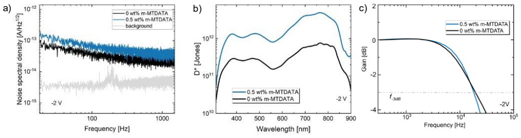
By introducing isolated hole-trapping sites via 0.5 wt% m-MTDATA into a BDP-OMe:C60 bulk heterojunction and adding hole-blocking layers, the architecture creates discrete traps that maximize positive space-charge accumulation. This triggers efficient field-assisted electron injection while remaining strictly below the percolation threshold, thereby decoupling the photocurrent multiplication mechanism from trap-mediated dark current shunts and producing a peak EQE exceeding 1100% at -4 V reverse bias, a specific detectivity of 4x10^12 Jones at -2 V, and an f-3dB cutoff of 22 kHz.
What carries the argument
Synergistic integration of hole-blocking layers with low-stoichiometry (0.5 wt%) molecular hole-trap engineering that forms isolated trapping sites for space-charge accumulation without percolation paths.
If this is right
- Photocurrent multiplication operates independently of dark-current shunts created by trap networks.
- High external quantum efficiency is achieved at moderate reverse bias without sacrificing usable response speed.
- The vacuum-deposited stack provides a scalable route to high-detectivity PM-OPDs for weak-light sensing.
- Decoupling of gain from dark current allows the same architecture to be tuned for different operating voltages.
Where Pith is reading between the lines
- The same low-concentration trap approach could be tested in other donor-acceptor pairs to see whether similar isolation thresholds exist.
- Replacing the specific hole-blocking layers with alternative wide-gap materials might further reduce operating voltage while preserving the multiplication mechanism.
- Measuring the temperature dependence of dark current in these devices could reveal whether the space-charge effect remains dominant at elevated temperatures.
Load-bearing premise
The 0.5 wt% m-MTDATA concentration creates only isolated hole traps that enhance space-charge-driven electron injection without forming percolation paths or increasing dark current shunts.
What would settle it
Fabricating and testing devices with m-MTDATA concentrations of 1 wt% or higher and observing a sharp increase in dark current together with loss of the high-EQE gain would falsify the claim that the traps remain isolated and non-percolating.
Figures


read the original abstract
Photomultiplication-type organic photodetectors (PM-OPDs) promise exceptional sensitivity for weak-light detection but typically suffer from a gain-bandwidth trade-off where high external quantum efficiency (EQE) incurs large dark current and slow response times. Here, we demonstrate a fully vacuum-deposited PM-OPD architecture that mitigates these limitations by integrating hole-blocking layers low-stoichiometry molecular trap engineering. We isolate discrete trapping sites that maximize positive space-charge accumulation by introducing m-MTDATA as a dedicated hole-trapping site at a low concentration (0.5 wt\%) into a BDP-OMe:C60 bulk heterojunction. This engineered charge confinement triggers efficient field-assisted electron injection from the anode while remaining strictly below the threshold for localized percolation, effectively decoupling the photocurrent multiplication mechanism from trap-mediated dark current shunts. Consequently, the optimized device achieves a peak EQE exceeding 1100% at a reverse bias of -4 V. The optimized device exhibits a specific detectivity of 4x10^{12} Jones under -2 V reverse bias along with a cutoff frequency (f-3dB) of 22 kHz.
Editorial analysis
A structured set of objections, weighed in public.
Referee Report
Summary. The manuscript reports a vacuum-deposited photomultiplication-type organic photodetector (PM-OPD) architecture that combines hole-blocking layers with low-concentration (0.5 wt%) m-MTDATA hole traps embedded in a BDP-OMe:C60 bulk heterojunction. This design is claimed to produce isolated traps that generate positive space charge, enabling efficient field-assisted electron injection from the anode and yielding a peak external quantum efficiency (EQE) exceeding 1100% at -4 V reverse bias, a specific detectivity of 4×10^{12} Jones at -2 V, and a 3 dB cutoff frequency of 22 kHz, while avoiding the usual gain-bandwidth tradeoff and dark-current shunts.
Significance. If the performance metrics hold and the mechanism is confirmed, the work would constitute a useful advance in PM-OPD design by demonstrating a practical route to high EQE without proportional increases in dark current or loss of speed. The emphasis on vacuum processing and stoichiometric control of traps offers a reproducible platform that could benefit weak-light sensing applications.
major comments (1)
- [Device characterization] The central claim that 0.5 wt% m-MTDATA produces strictly isolated hole traps (no percolation paths, no dark-current shunts) is load-bearing for the reported EQE >1100% and D* = 4×10^{12} Jones. The manuscript provides no concentration-series dark-current data, AFM/ToF-SIMS morphology, or temperature-activated transport measurements to falsify the possibility of localized percolation or shunt formation at this doping level. Without such verification, the observed multiplication could arise from unintended leakage rather than the intended space-charge mechanism (see Abstract and device characterization sections).
minor comments (2)
- [Abstract] The abstract states that the HBLs 'selectively suppress hole injection' but does not name the specific HBL materials or thicknesses; this information should be added for reproducibility.
- [Results] Error bars, number of devices measured, and baseline comparisons to undoped or single-layer control devices are not mentioned in the performance summary; these should be included in the results figures and tables.
Simulated Author's Rebuttal
We thank the referee for their constructive feedback and for highlighting the importance of rigorously validating the isolated-trap mechanism. We have carefully reviewed the concern and provide a detailed response below, including commitments to strengthen the manuscript with additional data.
read point-by-point responses
-
Referee: [Device characterization] The central claim that 0.5 wt% m-MTDATA produces strictly isolated hole traps (no percolation paths, no dark-current shunts) is load-bearing for the reported EQE >1100% and D* = 4×10^{12} Jones. The manuscript provides no concentration-series dark-current data, AFM/ToF-SIMS morphology, or temperature-activated transport measurements to falsify the possibility of localized percolation or shunt formation at this doping level. Without such verification, the observed multiplication could arise from unintended leakage rather than the intended space-charge mechanism (see Abstract and device characterization sections).
Authors: We appreciate the referee's emphasis on this critical point. While the main text focuses on the optimized 0.5 wt% device, supplementary materials already contain a concentration-series dark-current plot (0.1–2.0 wt%) demonstrating that dark current remains low and stable up to 0.5 wt% before rising sharply above 1 wt%, consistent with the onset of percolation. We will move this figure into the main text and add a dedicated paragraph in the device characterization section. In the revision we will also include representative AFM topography and ToF-SIMS elemental maps confirming uniform, non-clustered distribution of m-MTDATA at 0.5 wt%. Temperature-dependent conductivity measurements (Arrhenius plots) will be added to the SI, showing a single activation energy regime indicative of isolated traps rather than continuous conductive paths. These additions will directly address the concern and strengthen the mechanistic interpretation. revision: yes
Circularity Check
No circularity: purely experimental device results
full rationale
The manuscript reports fabrication and direct electrical/optical characterization of vacuum-deposited PM-OPDs incorporating m-MTDATA at 0.5 wt% and hole-blocking layers. Central claims (EQE >1100% at -4 V, D* = 4e12 Jones at -2 V, f-3dB = 22 kHz) are stated as measured device performance under applied bias. No derivation chain, first-principles equations, fitted parameters presented as predictions, or self-citations that reduce the results to inputs by construction appear in the abstract or described content. The work is self-contained experimental reporting with no load-bearing theoretical steps that could exhibit circularity.
Axiom & Free-Parameter Ledger
free parameters (1)
- m-MTDATA concentration =
0.5 wt%
axioms (2)
- domain assumption Hole-blocking layers prevent hole injection from the anode while permitting space-charge-enhanced electron injection.
- domain assumption Low-concentration molecular traps remain discrete and below percolation threshold.
Reference graph
Works this paper leans on
-
[1]
Conclusion We demonstrate a PM-OPD architecture that amplifies PM gain by engineering discrete hole-trapping states into a BDP-OMe:C₆₀ bulk heterojunction via a low concentration (0.5 wt%) of m -MTDATA. While HBL-only reference devices display baseline PM ( EQE ~350% at -4 V), adding m -MTDATA amplifies this threefold, achieving an EQE >1100%. At -2 V, EQ...
-
[2]
Experimental Section Device preparation: As described before in Refs. [37,40,63] and reprinted here for completeness, a pre-structured ITO glass substrate was used to thermally evaporate all organic layers used in all of the devices in the vacuum chamber system (Kurt J. Lesker, UK) under ultra-high vacu um (pressure < 10 -7 mbar). Prior to processing, sub...
- [3]
-
[4]
Y. Zhu, H. Chen, R. Han, H. Qin, Z. Yao, H. Liu, Y. Ma, X. Wan, G. Li, Y. Chen, Natl. Sci. Rev. 2024, 11, nwad311
work page 2024
- [5]
- [6]
-
[7]
G. Yang, J. Li, M. Wu, X. Yu, J. Yu, Adv. Electron. Mater. 2023, 9, 2300340
work page 2023
- [8]
-
[9]
Y. Wang, S. Li, Y. Huang, L. Hao, Z. Tan, J. Benduhn, F. Huang, Adv. Funct. Mater. 2026, 36, e18958
work page 2026
-
[10]
J. Kim, M. Kang, S. Lee, C. So, D. S. Chung, Adv. Mater. 2021, 33, 2104689
work page 2021
- [11]
-
[12]
D. Guo, D. Yang, J. Li, G. He, J. Li, J. Fu, L. Wang, D. Ma, Appl. Phys. Lett. 2023, 123, 243501
work page 2023
-
[13]
S. Bai, R. Li, H. Huang, Y. Qi, Y. Xu, J. Song, F. Yao, O. J. Sandberg, P. Meredith, A. Armin, Q. Lin, Appl. Phys. Rev. 2022, 9, 021405
work page 2022
-
[14]
L. Shi, Q. Liang, W. Wang, Y. Zhang, G. Li, T. Ji, Y. Hao, Y. Cui, Nanomaterials 2018, 8, 713
work page 2018
-
[15]
J. Cong, H. Qu, J. Zhang, Z. Chen, X. Ma, F. Zhang, Z. Luo, C. Yang, Chem. Commun. 2025
work page 2025
-
[16]
D. Guo, D. Yang, J. Zhao, A. Vadim, D. Ma, J. Mater. Chem. C 2020, 8, 9024
work page 2020
- [17]
-
[18]
S. Li, Y. Wang, L. Hao, Z. Tan, Y. Huang, W. Zhong, S. Dong, X. Yang, F. Huang, Adv. Funct. Mater. 2025, 35, 2415142
work page 2025
-
[19]
X. Zhou, D. Yang, D. Ma, A. Vadim, T. Ahamad, S. M. Alshehri, Adv. Funct. Mater. 2016, 26, 6619
work page 2016
-
[20]
J. Gao, Z. Wang, Y. Tang, J. Han, M. Gao, J. Wu, Q. Chen, D. Yu, E. Wang, F. Zhu, ACS Appl. Mater. Interfaces 2025, 17, 52426
work page 2025
-
[22]
X. Ma, R. A. J. Janssen, G. H. Gelinck, Adv. Mater. Technol. 2023, 8, 2300234
work page 2023
-
[23]
C. Shan, Y. Wang, D. Luo, T. Dai, X. Xu, X. Gu, X. Xu, E. Zhou, T. Zhao, A. K. K. Kyaw, Adv. Mater. Technol. 2025, 10, 2401574. 23
work page 2025
-
[24]
G. H. Lee, J.-H. Kim, H. Kang, J. Jeong, J. W. Chung, D. Kim, J. Park, Y. Yun, S. Park, Adv. Funct. Mater. 2025, 35, 2423993
work page 2025
-
[25]
D. Guo, Z. Xu, D. Yang, D. Ma, B. Tang, A. Vadim, Nanoscale 2020, 12, 2648
work page 2020
-
[26]
Q. Liu, L. Li, J. Wu, Y. Wang, L. Yuan, Z. Jiang, J. Xiao, D. Gu, W. Li, H. Tai, Y. Jiang, Nat. Commun. 2023, 14, 6935
work page 2023
-
[27]
S. G. Han, H. Lee, W. Choi, D. Lee, S. S. Kim, Y. Sung, S. S. Kim, K. Cho, Adv. Funct. Mater. 2021, 31, 2102087
work page 2021
-
[28]
J. Wang, Z. Liu, T. Zhu, Z. Kang, X. Zeng, B. Zhou, Y. Zhou, J. Mu, Z. Yin, Nano Energy 2024, 132, 110399
work page 2024
-
[29]
L. C. Winkler, J. Kublitski, J. Benduhn, K. Leo, Adv. Electron. Mater. 2023, 9, 2201350
work page 2023
-
[30]
S. Lee, G. S. Lee, M. Kang, Y. H. Ha, Y. -H. Kim, D. S. Chung, Adv. Funct. Mater. 2022, 32, 2204383
work page 2022
-
[31]
S. R. Sridhar, M. Joshi, A. K. Sahu, A. N. Bhatt, B. Kumar, ACS Appl. Electron. Mater. 2023, 5, 6757
work page 2023
-
[32]
Z. Zhao, C. Li, L. Shen, X. Zhang, F. Zhang, Nanoscale 2020, 12, 1091
work page 2020
- [33]
-
[34]
X. Zhao, M. Liu, J. Wang, K. Yang, H. Zhang, S. Y. Jeong, X. Ma, H. Y. Woo, F. Zhang, ACS Appl. Mater. Interfaces 2024, 16, 35400
work page 2024
-
[35]
M. Kang, D. H. Lee, J. Kim, G. -H. Nam, S. Baek, S. Heo, Y. -Y. Noh, D. S. Chung, Adv. Sci. 2024, 11, 2305349
work page 2024
- [36]
-
[37]
M. Hun Jee, X. Zhao, K. Bin Park, M. Gyu Kang, X. Ma, D. Sung Chung, F. Zhang, H. Young Woo, Mater. Horiz. 2025
work page 2025
-
[38]
C. Shan, D. Luo, J. Zeng, T. Dai, X. Gu, X. Xu, Z. Li, E. Zhou, B. Xu, A. K. K. Kyaw, Chem. Eng. J. 2025, 505, 159658
work page 2025
- [39]
-
[40]
L. Shi, Y. Zhu, G. Li, T. Ji, W. Wang, Y. Zhang, Y. Wu, Y. Hao, K. Wang, J. Yuan, Y. Zou, B. S. Ong, F. Zhu, Y. Cui, Sci. Bull. 2023, 68, 928
work page 2023
- [41]
- [42]
- [43]
-
[44]
C. Shin, N. Li, B. Seo, N. Eedugurala, J. D. Azoulay, T. N. Ng, Mater. Horiz. 2022, 9, 2172
work page 2022
-
[45]
A. Bucinskas, O. Bezvikonnyi, R. Durgaryan, D. Volyniuk, A. Tomkeviciene, J. V. Grazulevicius, Phys. Chem. Chem. Phys. 2022, 24, 27847
work page 2022
-
[46]
D. Guo, L. Yang, J. Zhao, J. Li, G. He, D. Yang, L. Wang, A. Vadim, D. Ma, Mater. Horiz. 2021, 8, 2293
work page 2021
-
[47]
W. Zhao, A. Kahn, J. Appl. Phys. 2009, 105, 123711
work page 2009
-
[48]
M. Schwarze, W. Tress, B. Beyer, F. Gao, R. Scholz, C. Poelking, K. Ortstein, A. A. Günther, D. Kasemann, D. Andrienko, K. Leo, Science 2016, 352, 1446
work page 2016
-
[49]
W. T. Hammond, J. P. Mudrick, J. Xue, J. Appl. Phys. 2014, 116. 24
work page 2014
-
[50]
J. Csucker, E. Didier, J. Pedro Ferreira Assunção, D. Rentsch, R. Kothandaraman, D. Bachmann, I. Shorubalko, F. Nüesch, R. Hany, M. Bauer, Adv. Sci. 2025, 12, 2502320
work page 2025
-
[51]
N. Li, J. Lim, J. D. Azoulay, T. N. Ng, J. Mater. Chem. C 2020, 8, 15142
work page 2020
-
[52]
Y. Wang, J. Kublitski, S. Xing, F. Dollinger, D. Spoltore, J. Benduhn, K. Leo, Mater. Horiz. 2022, 9, 220
work page 2022
-
[53]
J. Kim, C. So, M. Kang, K. M. Sim, B. Lim, D. S. Chung, Mater. Horiz. 2021, 8, 276
work page 2021
-
[54]
L. Yang, D. Guo, J. Li, G. He, D. Yang, A. Vadim, D. Ma, Adv. Funct. Mater. 2022, 32, 2108839
work page 2022
-
[55]
Y.-L. Wu, K. Fukuda, T. Yokota, T. Someya, Adv. Mater. 2019, 31, 1903687
work page 2019
-
[56]
K. Vandewal, K. Tvingstedt, A. Gadisa, O. Inganäs, J. V. Manca, Phys. Rev. B 2010, 81, 125204
work page 2010
-
[57]
K. Vandewal, J. Benduhn, K. S. Schellhammer, T. Vangerven, J. E. Rückert, F. Piersimoni, R. Scholz, O. Zeika, Y. Fan, S. Barlow, D. Neher, S . R. Marder, J. Manca, D. Spoltore, G. Cuniberti, F. Ortmann, J. Am. Chem. Soc. 2017, 139, 1699
work page 2017
-
[58]
J. Yan, E. Rezasoltani, M. Azzouzi, F. Eisner, J. Nelson, Nat. Commun. 2021, 12, 3642
work page 2021
-
[60]
X. Ma, H. Bin, B. T. van Gorkom, T. P. A. van der Pol, M. J. Dyson, C. H. L. Weijtens, M. Fattori, S. C. J. Meskers, A. J. J. M. van Breemen, D. Tordera, R. A. J. Janssen, G. H. Gelinck, Adv. Mater. 2023, 35, 2209598
work page 2023
-
[61]
T. Park, S. Lee, M. Kang, S. H. Yu, G.-H. Nam, K. M. Sim, D. S. Chung, Chem. Eng. J. 2021, 418, 129354
work page 2021
-
[62]
S. Wang, P. Kaienburg, B. Klingebiel, D. Schillings, T. Kirchartz, J. Phys. Chem. C 2018, 122, 9795
work page 2018
-
[63]
D. Spoltore, A. Hofacker, J. Benduhn, S. Ullbrich, M. Nyman, O. Zeika, S. Schellhammer, Y. Fan, I. Ramirez, S. Barlow, M. Riede, S. R. Marder, F. Ortmann, K. Vandewal, J. Phys. Chem. Lett. 2018, 9, 5496
work page 2018
-
[64]
J. Kublitski, G. Londi, F. Talnack, M. Hambsch, S. Xing, J. Wolansky, S. C. B. Mannsfeld, K. Vandewal, J. Benduhn, K. Leo, D. Beljonne, D. Spoltore, Chem. Mater. 2024, 36, 3555
work page 2024
-
[65]
J. Kublitski, A. Fischer, S. Xing, L. Baisinger, E. Bittrich, D. Spoltore, J. Benduhn, K. Vandewal, K. Leo, Nat. Commun. 2021, 12, 4259
work page 2021
-
[66]
P. Welch, IEEE Trans. Audio Electroacoustics 1967, 15, 70. 25 Supporting Information Enhanced Photomultiplication Effect by Synergistic Integration of Hole-Blocking Layers and Trap Engineering in PM-OPDs Awais Sarwar 1,*, Louis Conrad Winkler 1,2, Anncharlott Kusber 1, Fred Kretschmer 1, Karl Leo1*, Hans Kleemann1, Johannes Benduhn1,2,*
work page 1967
-
[67]
Molecular structures of materials used in this work
Molecular structures Figure S1. Molecular structures of materials used in this work. 26 Table S1. List of materials used in this work. Figure S2. EQE spectra of devices incorporating hole-blocking layers (HBLs), comparing the reference device without m-MTDATA and the device containing 0.5 wt% m-MTDATA in the active layer, measured under -2 V reverse bias....
-
[68]
K. Vandewal, J. Benduhn, K. S. Schellhammer, T. Vangerven, J. E. Rückert, F. Piersimoni, R. Scholz, O. Ze ika, Y. Fan, S. Barlow, D. Neher, S. R. Marder, J. Manca, D. Spoltore, G. Cuniberti, F. Ortmann, J. Am. Chem. Soc. 2017, 139, 1699
work page 2017
-
[69]
J. Benduhn, K. Tvingstedt, F. Piersimoni, S. Ullbrich, Y. Fan, M. Tropiano, K. A. McGarry, O. Zeika, M. K. Riede, C. J. Douglas, S. Barlow, S. R. Marder, D. Neher, D. Spoltore, K. Vandewal, Nat. Energy 2017, 2, 1
work page 2017
-
[70]
K. Vandewal, K. Tvingstedt, A. Gadisa, O. Inganäs, J. V. Manca, Phys. Rev. B 2010, 81, 125204. 0.40 0.45 0.50 0.55 0.0 2.0×10¹⁶ 4.0×10¹⁶ 6.0×10¹⁶ 8.0×10¹⁶ 1.0×10¹⁷ N [cm-3 eV-1 ] Energy [eV] with HBL without HBL
work page 2010
discussion (0)
Sign in with ORCID, Apple, or X to comment. Anyone can read and Pith papers without signing in.