Space-Charge Effects in Silicon Reconfigurable Nonlinear-Processing Units
Pith reviewed 2026-05-20 21:21 UTC · model grok-4.3
The pith
Space charge from injected carriers competing with fixed dopants governs nonlinearity in silicon reconfigurable units
A machine-rendered reading of the paper's core claim, the machinery that carries it, and where it could break.
Core claim
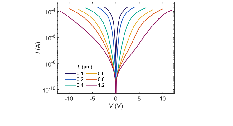
The central claim is that transport is governed by space charge. Interface trap states strongly suppress the equilibrium carrier density, while the functional nonlinearity arises from the voltage-dependent competition between injected mobile carriers and fixed ionized background dopants. The resulting non-equilibrium transport exhibits a transition from an Ohmic regime to a strongly nonlinear regime, and ultimately to a velocity-saturation space-charge-limited current regime, as evidenced by the observed voltage and length scaling. Background doping of opposite polarity controls the onset and strength of the nonlinearity, leading to behavior exceeding the quadratic dependence of the Mott-Gar
What carries the argument
Voltage-dependent competition between injected mobile carriers and fixed ionized background dopants that produces space-charge-limited current
If this is right
- Background doping of chosen polarity and density can tune the onset and strength of the nonlinearity.
- Device response is set by the spatial distribution of injected carriers and fixed charge rather than by disorder.
- Reproducible, scalable implementations become possible in standard CMOS processes.
- The same physical picture applies across multiple device lengths and temperatures without invoking hopping transport.
Where Pith is reading between the lines
- The same carrier-dopant competition could be engineered in other semiconductors to produce similar tunable nonlinear elements.
- Direct embedding of these units alongside conventional CMOS transistors would enable compact hybrid nonlinear circuits.
- Systematic variation of doping levels would map the precise boundaries between the observed transport regimes.
Load-bearing premise
Interface trap states are the dominant mechanism suppressing equilibrium carrier density and drift-diffusion simulations capture the internal field profile without additional disorder effects.
What would settle it
A measurement showing transport scaling or temperature dependence inconsistent with space-charge-limited current, such as strong hopping signatures or length-independent current that mismatches the simulated field profile.
Figures


read the original abstract
Reconfigurable nonlinear-processing units (RNPUs) are multi-terminal electronic devices that act as computational primitives, exploiting intrinsic nonlinear charge transport combined with electrostatic tunability. Silicon-based realizations provide a scalable and technologically relevant platform, yet the physical origin of their room-temperature nonlinearity has remained insufficiently understood. Here, we investigate charge transport using temperature- and length-dependent current-voltage measurements on physical devices, complemented by drift-diffusion simulations, and show that transport is governed by space charge. Interface trap states strongly suppress the equilibrium carrier density, while the functional nonlinearity arises from the voltage-dependent competition between injected mobile carriers and fixed ionized background dopants. The resulting non-equilibrium transport exhibits a transition from an Ohmic regime to a strongly nonlinear regime, and ultimately to a velocity-saturation space-charge-limited current regime, as evidenced by the observed voltage and length scaling. We further show that background doping of opposite polarity to the injected carriers controls the onset and strength of the nonlinearity, leading to behavior exceeding the quadratic dependence of the classical Mott-Gurney law. Agreement between experiment and simulation supports that the spatial distribution of injected carriers and fixed charge governs the internal electric-field profile and device response. These results establish a physical framework for silicon-based RNPUs without requiring disorder or hopping transport, and provide design guidelines for reproducible, scalable, and CMOS-compatible implementations of nonlinear computing hardware.
Editorial analysis
A structured set of objections, weighed in public.
Referee Report
Summary. The paper claims that charge transport in silicon reconfigurable nonlinear-processing units is governed by space-charge effects. Interface trap states suppress equilibrium carrier density, while nonlinearity arises from voltage-dependent competition between injected mobile carriers and fixed ionized dopants of opposite polarity. This produces transitions from Ohmic to strongly nonlinear to velocity-saturation space-charge-limited regimes, as shown by temperature- and length-dependent I-V data and drift-diffusion simulations that match the observed voltage and length scaling.
Significance. If the central interpretation holds, the work supplies a concrete physical framework for silicon RNPUs that avoids disorder or hopping transport and supplies design rules based on background doping polarity and magnitude. The combination of length- and temperature-dependent scaling data with simulation agreement is a positive feature that could support reproducible, CMOS-compatible nonlinear hardware.
major comments (2)
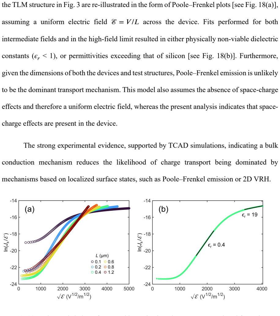
- [Abstract / physical-origin paragraph] Abstract and physical-origin paragraph: the assertion that interface trap states are the dominant suppressor of equilibrium carrier density is inferred from simulation agreement rather than direct measurement (no C-V or DLTS data are cited). This attribution is load-bearing for the claim that nonlinearity specifically results from injected-carrier competition with fixed dopants rather than alternative mechanisms such as contact injection or bulk disorder.
- [Drift-diffusion simulation section] Drift-diffusion simulation section: the manuscript should state explicitly whether the trap density at interfaces and background doping concentration were independently measured or adjusted to fit the I-V curves. If these remain free parameters, the reported agreement with experiment does not yet constitute an independent test of the space-charge picture.
minor comments (2)
- [Figures] Figure captions and axis labels should explicitly indicate whether plotted currents are for single devices or averages over multiple devices, and whether length scaling is performed at fixed temperature or vice versa.
- [Abstract] The abstract states that the nonlinearity exceeds the quadratic Mott-Gurney dependence; a brief quantitative comparison (e.g., extracted exponent versus classical 2) would strengthen this point.
Simulated Author's Rebuttal
We thank the referee for the positive assessment of our work and for the constructive major comments, which help clarify the evidential basis for our interpretation of space-charge-limited transport in silicon RNPUs. We address each point below and will revise the manuscript accordingly to improve transparency regarding the role of interface traps and the status of simulation parameters.
read point-by-point responses
-
Referee: [Abstract / physical-origin paragraph] Abstract and physical-origin paragraph: the assertion that interface trap states are the dominant suppressor of equilibrium carrier density is inferred from simulation agreement rather than direct measurement (no C-V or DLTS data are cited). This attribution is load-bearing for the claim that nonlinearity specifically results from injected-carrier competition with fixed dopants rather than alternative mechanisms such as contact injection or bulk disorder.
Authors: We agree that the attribution of equilibrium carrier suppression to interface trap states rests on consistency with drift-diffusion simulations rather than direct spectroscopic or capacitance measurements. The temperature- and length-dependent I-V scaling data, together with the observed polarity dependence on background doping, provide indirect support for this picture and help rule out bulk disorder or simple contact-limited injection as dominant alternatives. In the revised manuscript we will explicitly qualify the abstract and physical-origin section to state that trap densities are inferred from transport modeling within literature-typical ranges for Si/SiO2 interfaces, and we will add a short paragraph discussing why the data are less consistent with hopping or disorder-based mechanisms. We will also note the desirability of future C-V or DLTS characterization. revision: yes
-
Referee: [Drift-diffusion simulation section] Drift-diffusion simulation section: the manuscript should state explicitly whether the trap density at interfaces and background doping concentration were independently measured or adjusted to fit the I-V curves. If these remain free parameters, the reported agreement with experiment does not yet constitute an independent test of the space-charge picture.
Authors: We accept this clarification request. Background doping levels are taken from the foundry wafer specifications (independently determined by resistivity measurements), while interface trap densities are varied within physically plausible bounds (10^11–10^12 cm^-2 eV^-1) to obtain quantitative agreement with the measured current magnitudes. The voltage and length scaling of the Ohmic-to-nonlinear and velocity-saturation transitions, however, follow directly from the space-charge framework and are not fitted parameters. In the revised simulation section we will state these distinctions explicitly, emphasize that the scaling behaviors constitute the primary test of the model, and acknowledge that the absolute current values involve some parameter adjustment. revision: yes
Circularity Check
No significant circularity; claims rest on independent experimental data and simulations.
full rationale
The paper's derivation proceeds from temperature- and length-dependent current-voltage measurements on fabricated devices, which exhibit specific voltage and length scaling. These data are interpreted via drift-diffusion simulations that incorporate interface traps and background doping to reproduce the observed Ohmic-to-nonlinear-to-velocity-saturation transitions. Agreement between measured scaling and simulated internal field profiles is presented as supporting evidence rather than as a definitional input. No equations reduce to their own fitted parameters by construction, no predictions are statistically forced from subsets of the same data, and no load-bearing steps rely on self-citations or imported uniqueness theorems. The central attribution to space-charge effects is therefore externally grounded in device measurements and is not equivalent to its inputs.
Axiom & Free-Parameter Ledger
free parameters (2)
- trap density at interfaces
- background doping concentration
axioms (1)
- domain assumption Drift-diffusion equations adequately describe charge transport in these micron-scale silicon devices at room temperature.
Lean theorems connected to this paper
-
IndisputableMonolith/Cost/FunctionalEquation.leanwashburn_uniqueness_aczel unclear?
unclearRelation between the paper passage and the cited Recognition theorem.
transport is governed by space charge... transition from an Ohmic regime to a strongly nonlinear regime, and ultimately to a velocity-saturation space-charge-limited current regime... J_SCLC ∝ μϵ V^2 / L^2 ... J_SCLC-VS ∝ v_sat ϵ V / L
-
IndisputableMonolith/Foundation/RealityFromDistinction.leanreality_from_one_distinction unclear?
unclearRelation between the paper passage and the cited Recognition theorem.
Agreement between experiment and simulation supports that the spatial distribution of injected carriers and fixed charge governs the internal electric-field profile
What do these tags mean?
- matches
- The paper's claim is directly supported by a theorem in the formal canon.
- supports
- The theorem supports part of the paper's argument, but the paper may add assumptions or extra steps.
- extends
- The paper goes beyond the formal theorem; the theorem is a base layer rather than the whole result.
- uses
- The paper appears to rely on the theorem as machinery.
- contradicts
- The paper's claim conflicts with a theorem or certificate in the canon.
- unclear
- Pith found a possible connection, but the passage is too broad, indirect, or ambiguous to say the theorem truly supports the claim.
Reference graph
Works this paper leans on
-
[1]
J. D. Kendall and S. Kumar, The building blocks of a brain-inspired computer, Appl. Phys. Rev. 7, 011305 (2020)
work page 2020
-
[2]
M. A. Zidan, J. P. Strachan, and W. D. Lu, The future of electronics based on memristive systems, Nat. Electron. 1, 22 (2018)
work page 2018
-
[3]
M. Xu, X. Chen, Y . Guo, Y . Wang, D. Qiu, X. Du, Y . Cui, X. Wang, and J. Xiong, Reconfigurable Neuromorphic Computing: Materials, Devices, and Integration, Adv. Mater. 35, 2301063 (2023)
work page 2023
-
[4]
M.-K. Song et al., Recent advances and future prospects for memristive materials, devices, and systems, ACS Nano 17, 11994 (2023)
work page 2023
-
[5]
S. Choi, T. Moon, G. Wang, and J. J. Yang, Filament-free memristors for computing, Nano Converg. 10, 58 (2023)
work page 2023
- [6]
-
[7]
C. Pan et al., Reconfigurable logic and neuromorphic circuits based on electrically tunable two-dimensional homojunctions, Nat. Electron. 3, 383 (2020)
work page 2020
-
[8]
T. Mikolajick et al., Reconfigurable field effect transistors: a technology enablers perspective, Solid-State Electron. 194, 108381 (2022)
work page 2022
-
[9]
D. Guo, M. Jia, Y . Wang, X. Liu, X. Zhang, Y . Shi, W. Hu, A. Yu, Z. L. Wang, and J. Zhai, Neuromorphic Silicon‐Based Capacitive‐Tunneling Junction, Adv. Mater. 2416643 (2025)
work page 2025
-
[10]
T. Chen, J. van Gelder, B. van de Ven, S. V . Amitonov, B. de Wilde, H.-C. Ruiz Euler, H. Broersma, P. A. Bobbert, F. A. Zwanenburg, and W. G. van der Wiel, Classification with a disordered dopant-atom network in silicon, Nature 577, 7790 (2020). 55
work page 2020
-
[11]
H.-C. Ruiz Euler, M. N. Boon, J. T. Wildeboer, B. van de Ven, T. Chen, H. Broersma, P. A. Bobbert, and W. G. van der Wiel, A deep-learning approach to realizing functionality in nanoelectronic devices, Nat. Nanotechnol. 15, 992 (2020)
work page 2020
-
[12]
H.-C. Ruiz-Euler, U. Alegre-Ibarra, B. van de Ven, H. Broersma, P. A. Bobbert, and W. G. van der Wiel, Dopant network processing units: towards efficient neural network emulators with high-capacity nanoelectronic nodes, Neuromorphic Comput. Eng. 1, 024002 (2021)
work page 2021
-
[13]
M. Zolfagharinejad, J. Büchel, L. Cassola, S. Kinge, G. S. Syed, A. Sebastian, and W. G. van der Wiel, Analogue speech recognition based on physical computing, Nature 645, 886 (2025)
work page 2025
-
[14]
M. Escudero, M. Zolfagharinejad, S. van den Belt, N. Alachiotis, and W. G. van der Wiel, Physical Analog Kolmogorov-Arnold Networks Based on Reconfigurable Nonlinear-Processing Units, arXiv:2602.07518
work page internal anchor Pith review arXiv
-
[15]
F. Taglietti et al., Learning Nonlinear Heterogeneity in Physical Kolmogorov-Arnold Networks, arXiv:2601.15340
-
[16]
H. Tertilt, J. Bakker, M. Becker, B. de Wilde, I. Klanberg, B. J. Geurts, W. G. van der Wiel, A. Heuer, and P. A. Bobbert, Hopping-transport mechanism for reconfigurable logic in disordered dopant networks, Phys. Rev. Appl. 17, 064025 (2022)
work page 2022
-
[17]
H. Tertilt, J. Mensing, M. Becker, W. G. van der Wiel, P. A. Bobbert, and A. Heuer, Critical nonlinear aspects of hopping transport for reconfigurable logic in disordered dopant networks, Phys. Rev. Appl. 22, 024063 (2024)
work page 2024
-
[18]
T. Chen, J. van Gelder, B. van de Ven, S. V . Amitonov, B. de Wilde, H.-C. Ruiz Euler, H. Broersma, P. A. Bobbert, F. A. Zwanenburg, and W. G. van der Wiel, Author correction: classification with a disordered dopant atom network in silicon, Nature 639, E22 (2025). 56
work page 2025
-
[19]
R. K. Ray and H. Y . Fan, Impurity Conduction in Silicon, Phys. Rev. 121, 768 (1961)
work page 1961
-
[20]
W. N. Shafarman, D. W. Koon, and T. G. Castner, dc conductivity of arsenic-doped silicon near the metal-insulator transition, Phys. Rev. B 40, 1216 (1989)
work page 1989
- [21]
-
[22]
J. D. Plummer, M. Deal, and P. B. Griffin, Silicon VLSI Technology: Fundamentals, Practice and Modeling (Prentice hall, Upper Saddle River (N.J.), 2000)
work page 2000
- [23]
-
[24]
L. Ribar and R. Sepulchre, Neuromorphic control: designing multiscale mixed- feedback systems, IEEE Control Syst. Mag. 41, 34 (2021)
work page 2021
-
[25]
M. Dragoman and D. Dragoman, Negative differential resistance in novel nanoscale devices, Solid-State Electron. 197, 108464 (2022)
work page 2022
-
[26]
H. Lu et al., Negative differential resistance in memristive systems: historical evolution, mechanisms and neuromorphic applications of niobium oxide devices, Nanoscale 17, 20606 (2025)
work page 2025
-
[27]
Kareem, Manuscript in Preparation, (unpublished)
J. Kareem, Manuscript in Preparation, (unpublished)
-
[28]
C. R. Helms and E. H. Poindexter, The silicon-silicon dioxide system: its microstructure and imperfections, Rep. Prog. Phys. 57, 791 (1994)
work page 1994
-
[29]
P. M. Lenahan, T. D. Mishima, J. Jumper, T. N. Fogarty, and R. T. Wilkins, Direct experimental evidence for atomic scale structural changes involved in the interface-trap transformation process, IEEE Trans. Nucl. Sci. 48, 2131 (2001). 57
work page 2001
-
[30]
S. T. Chang, J. K. Wu, and S. A. Lyon, Amphoteric defects at the Si-SiO2 interface, Appl. Phys. Lett. 48, 662 (1986)
work page 1986
-
[31]
H. Hasegawa, T. Sato, S. Kasai, B. Adamowicz, and T. Hashizume, Dynamics and control of recombination process at semiconductor surfaces, interfaces and nano- structures, Sol. Energy 80, 629 (2006)
work page 2006
-
[32]
J. B. Varley, J. R. Weber, A. Janotti, and C. G. van de Walle, Dangling bonds, the charge neutrality level, and band alignment in semiconductors, J. Appl. Phys. 135, 075703 (2024)
work page 2024
-
[33]
Victory Device (Version 1.24.0.R) (Silvaco, Inc., Santa Clara, CA, USA, 2024)
work page 2024
-
[34]
S. M. Sze and K. K. Ng, Physics of Semiconductor Devices, 3rd ed. (Wiley- Interscience, Hoboken, N.J, 2007)
work page 2007
-
[35]
G. T. Wright, Mechanisms of space-charge-limited current in solids, Solid-State Electron. 2, 165 (1961)
work page 1961
-
[36]
A. A. Grinberg and S. Luryi, Space-charge-limited current and capacitance in double- junction diodes, J. Appl. Phys. 61, 1181 (1987)
work page 1987
-
[37]
J. A. Geurst, Theory of space-charge-limited currents in thin semiconductor layers, Phys. Status Solidi B 15, 107 (1966)
work page 1966
-
[38]
A. A. Grinberg, S. Luryi, M. R. Pinto, and N. L. Schryer, Space-charge-limited current in a film, IEEE Trans. Electron Devices 36, 1162 (1989)
work page 1989
-
[39]
M. A. Lampert and P. Mark, Current Injection in Solids (Academic Press, New York, 1970)
work page 1970
-
[40]
Rose, Space-Charge-Limited Currents in Solids, Phys
A. Rose, Space-Charge-Limited Currents in Solids, Phys. Rev. 97, 1538 (1955)
work page 1955
-
[41]
D. M. Caughey and R. E. Thomas, Carrier mobilities in silicon empirically related to doping and field, Proc. IEEE 55, 2192 (1967). 58
work page 1967
- [42]
-
[43]
Victory Device User Manual (Silvaco, Inc., Santa Clara, CA, USA, 2024)
work page 2024
-
[44]
D. B. M. Klaassen, A unified mobility model for device simulation— I. Model equations and concentration dependence, Solid-State Electron. 35, 953 (1992)
work page 1992
-
[45]
G. S. Oehrlein, Dry etching damage of silicon: A review, Mater. Sci. Eng. B 4, 441 (1989)
work page 1989
-
[46]
J. C. Mikkelsen and I.-W. Wu, Severe loss of dopant activity due to CHF3+CO2 reactive ion etch damage, Appl. Phys. Lett. 49, 103 (1986)
work page 1986
-
[47]
J. M. Heddleson, M. W. Horn, S. J. Fonash, and D. C. Nguyen, Effects of dry etching on the electrical properties of silicon, J. Vac. Sci. Technol. B Microelectron. Process. Phenom. 6, 280 (1988)
work page 1988
-
[48]
P. Mark and W. Helfrich, Space-charge-limited currents in organic crystals, J. Appl. Phys. 33, 205 (1962)
work page 1962
-
[49]
Nikolka et al., High-mobility, trap-free charge transport in conjugated polymer diodes, Nat
M. Nikolka et al., High-mobility, trap-free charge transport in conjugated polymer diodes, Nat. Commun. 10, 2122 (2019)
work page 2019
-
[50]
M. Sajedi Alvar, P. W. M. Blom, and G.-J. A. H. Wetzelaer, Space-charge-limited electron and hole currents in hybrid organic-inorganic perovskites, Nat. Commun. 11, 4023 (2020)
work page 2020
-
[51]
V . M. Le Corre, E. A. Duijnstee, O. El Tambouli, J. M. Ball, H. J. Snaith, J. Lim, and L. J. A. Koster, Revealing charge carrier mobility and defect densities in metal halide perovskites via space-charge-limited current measurements, ACS Energy Lett. 6, 1087 (2021). 59
work page 2021
- [52]
-
[53]
Space-Charge Effects in Silicon Reconfigurable Nonlinear- Processing Units,
J. Kareem, L. Cassola, R. J. C. Cool, J. I. van Slooten, P. A. Bobbert, and W. G. van der Wiel, Code and Data for “Space-Charge Effects in Silicon Reconfigurable Nonlinear- Processing Units,” https://doi.org/10.5281/ZENODO.20259202
- [54]
-
[55]
T. E. F. M. Standaert, C. Hedlund, E. A. Joseph, G. S. Oehrlein, and T. J. Dalton, Role of fluorocarbon film formation in the etching of silicon, silicon dioxide, silicon nitride, and amorphous hydrogenated silicon carbide, J. Vac. Sci. Technol. Vac. Surf. Films 22, 53 (2004)
work page 2004
-
[56]
A. Efremov, B. J. Lee, and K.-H. Kwon, On Relationships between Gas-Phase Chemistry and Reactive Ion Etching Kinetics for Silicon-Based Thin Films (SiC, SiO2 and SixNy) in Multi-Component Fluorocarbon Gas Mixtures, Materials 14, 1432 (2021)
work page 2021
- [57]
-
[58]
S. K. Bose, C. P. Lawrence, Z. Liu, K. S. Makarenko, R. M. J. van Damme, H. J. Broersma, and W. G. van der Wiel, Evolution of a designless nanoparticle network into reconfigurable Boolean logic, Nat. Nanotechnol. 10, 1048 (2015)
work page 2015
- [59]
-
[60]
C. Lombardi, S. Manzini, A. Saporito, and M. Vanzi, A physically based mobility model for numerical simulation of nonplanar devices, IEEE Trans. Comput.-Aided Des. Integr. Circuits Syst. 7, 1164 (1988)
work page 1988
-
[61]
D. B. M. Klaassen, A unified mobility model for device simulation— II. Temperature dependence of carrier mobility and lifetime, Solid-State Electron. 35, 961 (1992)
work page 1992
-
[62]
R. M. Hill, Poole-Frenkel conduction in amorphous solids, Philos. Mag. 23, 59 (1971)
work page 1971
discussion (0)
Sign in with ORCID, Apple, or X to comment. Anyone can read and Pith papers without signing in.