Hybrid-Integrated DFB-Laser-Coupled 1 * 8 Thin-Film Lithium Niobate Modulator Array for High-Speed Parallel Optical Transmitters
Pith reviewed 2026-05-21 01:56 UTC · model grok-4.3
The pith
A DFB laser passively butt-coupled to an eight-channel thin-film lithium niobate modulator array delivers over 40 GHz bandwidth per channel with uniform power split and low drive voltages.
A machine-rendered reading of the paper's core claim, the machinery that carries it, and where it could break.
Core claim
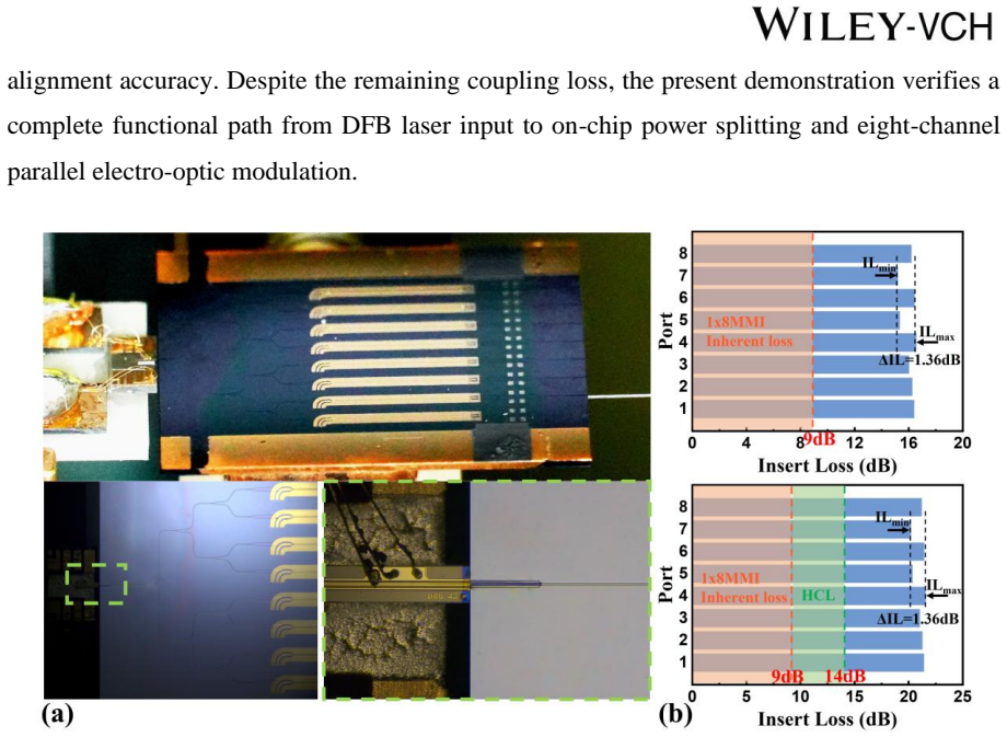
The authors fabricate and test a hybrid-integrated 1 × 8 TFLN modulator array that is passively butt-coupled to a distributed-feedback laser. A three-stage cascaded 1 × 2 multimode-interference splitter distributes optical power with at most 9.7 percent normalized deviation. Optimized traveling-wave electrodes on the Mach-Zehnder modulators produce 3 dB electro-optic bandwidths exceeding 40 GHz on every channel, half-wave voltages of 3.60–3.83 V (VπL products 2.52–2.68 V·cm for 7 mm length), and extinction ratios of approximately 25 dB. Total bare-chip insertion loss is 15.19–16.55 dB, with the laser bond adding roughly 5 dB coupling loss while preserving uniformity and performance.
What carries the argument
Passive butt-coupling of a DFB laser to a TFLN chip that integrates a cascaded MMI power splitter, eight traveling-wave Mach-Zehnder modulators, thermal tuning electrodes, and 50 Ω terminations.
If this is right
- All eight channels simultaneously support electro-optic bandwidths above 40 GHz.
- Optical power is split uniformly enough for parallel transmission with less than 10 percent deviation.
- Drive voltages stay in the 3.6–3.8 V range for a 7 mm interaction length.
- Extinction ratios near 25 dB are maintained across the array.
- The hybrid package forms a practical building block for compact high-speed parallel optical transmitters.
Where Pith is reading between the lines
- The same passive-coupling method could be tested with larger arrays to increase channel count without active alignment.
- Thermal electrodes already on the chip could be used to stabilize wavelengths for wavelength-division multiplexing.
- The low VπL product suggests the platform may scale to lower-power operation at higher symbol rates.
- Integration with driver electronics on the same substrate would further reduce footprint and parasitics.
Load-bearing premise
The passive butt-coupling of the DFB laser adds only the stated 5 dB loss and does not introduce distortions or performance degradation that would affect the measured bandwidth, voltage, or channel uniformity.
What would settle it
Direct measurement of any channel showing electro-optic 3 dB bandwidth below 40 GHz or coupling loss well above 5 dB accompanied by visible waveform distortion or loss of uniformity would falsify the central performance claims.
Figures


read the original abstract
Thin-film lithium niobate (TFLN) electro-optic modulators are attractive for high-speed optical interconnects, but scalable transmitter architectures require not only high modulation bandwidth but also multi-channel optical power distribution and practical laser-to-chip integration. Here, we demonstrate a hybrid-integrated 1 * 8 TFLN electro-optic modulator array passively butt-coupled to a 1550 nm distributed-feedback laser. The chip integrates a three-stage cascaded 1 * 2 multimode-interference splitter, spot-size converters, eight traveling-wave Mach-Zehnder modulators, thermal tuning electrodes, and on-chip 50 {\Omega} terminations. The cascaded splitter provides uniform optical power distribution with a maximum normalized power deviation of 9.7%, while the optimized electrodes enable electro-optic 3 dB bandwidths exceeding 40 GHz for all channels. The measured half-wave voltages are 3.60-3.83 V, corresponding to V{\pi}L products of 2.52-2.68 V cm for a 7 mm modulation length, and the extinction ratio reaches approximately 25 dB. The bare-chip insertion loss is 15.19-16.55 dB, and DFB laser bonding introduces an additional coupling loss of approximately 5 dB while preserving channel uniformity. These results establish a practical TFLN-based multi-channel modulator platform and represent a step toward compact hybrid-integrated optical transmitters for high-speed parallel interconnects.
Editorial analysis
A structured set of objections, weighed in public.
Referee Report
Summary. The manuscript reports the experimental demonstration of a hybrid-integrated 1×8 thin-film lithium niobate (TFLN) electro-optic modulator array passively butt-coupled to a 1550 nm DFB laser. The device integrates a cascaded 1×2 MMI splitter for optical power distribution, spot-size converters, eight traveling-wave Mach-Zehnder modulators with optimized electrodes and on-chip 50 Ω terminations, and thermal tuning electrodes. Key measured results include maximum normalized power deviation of 9.7%, electro-optic 3 dB bandwidths exceeding 40 GHz for all channels, half-wave voltages of 3.60–3.83 V (VπL products 2.52–2.68 V·cm for 7 mm length), extinction ratios of approximately 25 dB, bare-chip insertion loss of 15.19–16.55 dB, and an additional ~5 dB coupling loss from DFB bonding that preserves channel uniformity.
Significance. If the reported performance metrics are robust, this work provides a valuable experimental platform for compact, multi-channel TFLN-based optical transmitters suitable for high-speed parallel interconnects. The combination of uniform power splitting, high bandwidth, and practical hybrid laser integration addresses a key scalability challenge in TFLN photonics for data communications.
major comments (2)
- Abstract: The claim that DFB laser bonding 'preserves channel uniformity' and the overall electro-optic performance (including >40 GHz bandwidths) is not supported by any pre- versus post-bonding comparison of S21 electro-optic response, optical reflection spectra, or mode-mismatch analysis at the butt joint. Without such data, it is difficult to confirm that the headline bandwidth and VπL figures are attributable solely to the optimized electrodes rather than interface effects.
- Abstract: No error bars, standard deviations, or repeatability data are provided for the reported bandwidths, Vπ values, or power uniformity (9.7% deviation), nor is there discussion of fabrication tolerances or measurement uncertainties. This weakens the strength of the quantitative performance claims for a multi-channel device.
minor comments (1)
- Abstract: The notation '1 * 8' should be updated to the conventional '1×8' for clarity in the title and text.
Simulated Author's Rebuttal
We thank the referee for the careful review and constructive comments on our manuscript. We address each major comment point by point below, providing clarifications where possible and indicating revisions to the manuscript.
read point-by-point responses
-
Referee: Abstract: The claim that DFB laser bonding 'preserves channel uniformity' and the overall electro-optic performance (including >40 GHz bandwidths) is not supported by any pre- versus post-bonding comparison of S21 electro-optic response, optical reflection spectra, or mode-mismatch analysis at the butt joint. Without such data, it is difficult to confirm that the headline bandwidth and VπL figures are attributable solely to the optimized electrodes rather than interface effects.
Authors: We thank the referee for this important point. All reported electro-optic bandwidths exceeding 40 GHz, Vπ values, and the power uniformity of 9.7% maximum normalized deviation were measured on the fully hybrid-integrated device after passive butt-coupling of the DFB laser. The statement that bonding 'preserves channel uniformity' is based on post-bonding output power measurements across the eight channels, which reflect the performance of the on-chip cascaded MMI splitter with the additional ~5 dB coupling loss appearing as a common-mode effect due to the single laser source and uniform passive alignment to the spot-size converters. We agree that explicit pre- versus post-bonding S21 comparisons or mode-mismatch analysis would more conclusively isolate any interface contributions. Such comparative data is not available in our experimental dataset because the bonding step is permanent. We have revised the abstract and added clarifying text in the results section stating that all quantitative metrics refer to the bonded configuration and discussing why the butt-joint design is expected to have negligible impact on the traveling-wave electrode bandwidth. revision: partial
-
Referee: Abstract: No error bars, standard deviations, or repeatability data are provided for the reported bandwidths, Vπ values, or power uniformity (9.7% deviation), nor is there discussion of fabrication tolerances or measurement uncertainties. This weakens the strength of the quantitative performance claims for a multi-channel device.
Authors: We agree that the inclusion of statistical measures and uncertainty discussion would strengthen the presentation of our multi-channel results. In the revised manuscript we have added error bars to the electro-optic bandwidth and half-wave voltage data based on repeat measurements across channels and devices. We have also included a new paragraph discussing fabrication tolerances (e.g., variations in electrode geometry and MMI dimensions) and measurement uncertainties in the optical power and S21 characterizations. The reported 9.7% figure is the maximum observed normalized deviation in the characterized device. revision: yes
- Pre- versus post-bonding comparison of S21 electro-optic response, optical reflection spectra, or mode-mismatch analysis at the butt joint, as these paired measurements were not performed in the experiment.
Circularity Check
No significant circularity: experimental demonstration paper
full rationale
This is a pure experimental paper reporting measured performance of a fabricated hybrid-integrated TFLN modulator array. All central claims (EO bandwidth >40 GHz, VπL of 2.52-2.68 V·cm, extinction ratio ~25 dB, coupling loss ~5 dB, power uniformity 9.7%) are direct measurement results from the device under test. No derivations, fitted models presented as predictions, or self-referential equations exist. The work contains no load-bearing self-citations or ansatzes that reduce to inputs by construction; results are externally falsifiable via replication of the fabrication and measurement process.
Axiom & Free-Parameter Ledger
Reference graph
Works this paper leans on
-
[1]
Miller, D.A.B., Device Requirements for Optical Interconnects to Silicon Chips. Proceedings of the IEEE, 2009. 97(7): p. 1166-1185
work page 2009
-
[2]
Minkenberg, C., et al., Co-packaged datacenter optics: Opportunities and challenges. IET Optoelectronics, 2021. 15(2): p. 77-91
work page 2021
-
[3]
Zhou, X., et al., Silicon photonics for high-speed communications and photonic signal processing. npj Nanophotonics, 2024. 1(1): p. 27
work page 2024
-
[4]
Boes, A., et al., Lithium niobate photonics: Unlocking the electromagnetic spectrum. Science, 2023. 379(6627): p. eabj4396
work page 2023
-
[5]
Honardoost, A., K. Abdelsalam, and S. Fathpour, Rejuvenating a Versatile Photonic Material: Thin-Film Lithium Niobate. Laser & Photonics Reviews, 2020. 14(9): p. 2000088
work page 2020
-
[6]
Laser & Photonics Reviews, 2018
Boes, A., et al., Status and Potential of Lithium Niobate on Insulator (LNOI) for Photonic Integrated Circuits. Laser & Photonics Reviews, 2018. 12(4): p. 1700256
work page 2018
-
[7]
Advanced Photonics Research, 2023
Chen, G., et al., Compact and Efficient Thin-Film Lithium Niobate Modulators. Advanced Photonics Research, 2023. 4(12): p. 2300229
work page 2023
-
[8]
Wang, C., et al., Integrated lithium niobate electro-optic modulators operating at CMOS-compatible voltages. Nature, 2018. 562(7725): p. 101-104
work page 2018
-
[9]
Zhang, M., et al., Integrated lithium niobate electro-optic modulators: when performance meets scalability. Optica, 2021. 8(5): p. 652-667
work page 2021
-
[10]
Mercante, A.J., et al., Thin film lithium niobate electro-optic modulator with terahertz operating bandwidth. Optics Express, 2018. 26(11): p. 14810-14816
work page 2018
-
[11]
Li, M., et al., Lithium niobate photonic-crystal electro-optic modulator. Nature Communications, 2020. 11: p. 4123
work page 2020
-
[12]
Yu, M., et al., Integrated femtosecond pulse generator on thin-film lithium niobate. Nature, 2022. 612(7939): p. 252-258. 14
work page 2022
-
[13]
Mookherjea, S., V. Mere, and F. Valdez, Thin-film lithium niobate electro-optic modulators: To etch or not to etch. Applied Physics Letters, 2023. 122(12): p. 120501
work page 2023
-
[14]
Hou, S., et al., High-Speed Electro-Optic Modulators Based on Thin-Film Lithium Niobate. Nanomaterials, 2024. 14(10): p. 867
work page 2024
-
[15]
He, M., et al., High-performance hybrid silicon and lithium niobate Mach–Zehnder modulators for 100 Gbit s−1 and beyond. Nature Photonics, 2019. 13(5): p. 359-364
work page 2019
-
[16]
Chen, G., et al., High performance thin-film lithium niobate modulator on a silicon substrate using periodic capacitively loaded traveling-wave electrode. APL Photonics,
-
[17]
Xu, M., et al., High-performance coherent optical modulators based on thin-film lithium niobate platform. Nature Communications, 2020. 11(1): p. 3911
work page 2020
-
[18]
Valdez, F., et al., Integrated O- and C-band silicon-lithium niobate Mach-Zehnder modulators with 100 GHz bandwidth, low voltage, and low loss. Optics Express, 2023. 31(4): p. 5273-5289
work page 2023
-
[19]
Li, Q., et al., Ultra-broadband near- to mid-infrared electro-optic modulator on thin- film lithium niobate. Nature Communications, 2026. 17(1): p. 1138
work page 2026
-
[20]
Churaev, M., et al., A heterogeneously integrated lithium niobate-on-silicon nitride photonic platform. Nature Communications, 2023. 14(1): p. 3499
work page 2023
-
[21]
Snigirev, V., et al., Ultrafast tunable lasers using lithium niobate integrated photonics. Nature, 2023. 615(7952): p. 411-417
work page 2023
-
[22]
Shams-Ansari, A., et al., Electrically pumped laser transmitter integrated on thin-film lithium niobate. Optica, 2022. 9(4): p. 408-411
work page 2022
-
[23]
Huang, X., et al., Advanced Electrode Design for Low-Voltage High-Speed Thin-Film Lithium Niobate Modulators. IEEE Photonics Journal, 2021. 13(2): p. 1-9
work page 2021
-
[24]
Wu, R., et al., Long Low-Loss-Litium Niobate on Insulator Waveguides with Sub- Nanometer Surface Roughness. Nanomaterials, 2018. 8(11): p. 910
work page 2018
-
[25]
Wu, R., et al., Lithium niobate micro-disk resonators of quality factors above 107. Optics Letters, 2018. 43(17): p. 4116-4119
work page 2018
-
[26]
Wang, M., et al., Chemo-mechanical polish lithography: A pathway to low loss large- scale photonic integration on lithium niobate on insulator. Quantum Engineering,
-
[27]
Song, L., et al., Electro-optically tunable optical delay line with a continuous tuning range of ∼220 fs in thin-film lithium niobate. Optics Letters, 2023. 48(9): p. 2261- 2264
work page 2023
-
[28]
Gao, L., et al., Thin-film lithium niobate electro-optic isolator fabricated by photolithography assisted chemo-mechanical etching. Optics Letters, 2024. 49(3): p. 614-617
work page 2024
discussion (0)
Sign in with ORCID, Apple, or X to comment. Anyone can read and Pith papers without signing in.