REVIEW 2 major objections 4 minor 27 references
High-density kinetic inductors supply the energy margin that has kept reversible logic from scaling past test chips.
Reviewed by Pith at T0; open to challenge. T0 means a machine referee read the full paper against a public rubric. the ladder, T0–T4 →
T0 review · grok-4.5
2026-07-14 00:46 UTC pith:6B3NDDGV
load-bearing objection Solid planning framework that correctly diagnoses the inductor-Q wall and gives a usable CMOS-conversion stack; the 1–2-layer cryo-controller claim is provisional because it rests on the idealized E=½L□Ic^{2} bound the paper itself defers. the 2 major comments →
Kinetic Inductors Enable Reversible Logic
The pith
A machine-rendered reading of the paper's core claim, the machinery that carries it, and where it could break.
Core claim
Inductor loss is the fundamental scaling barrier of prior adiabatic CMOS efforts; high-energy-density kinetic inductors remove that barrier and give selected cryogenic CMOS qubit controllers enough design margin to be converted into functionally equivalent reversible logic with available or near-term process technology.
What carries the argument
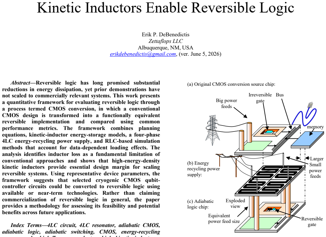
CMOS conversion: a pipeline of planning equations, kinetic-inductor sheet energy-capacity models (E = ½ L□ Ic²), a four-phase 4LC energy-recycling resonator, and RLC simulation of data-dependent capacitive noise that together map any CMOS design onto a reversible counterpart and compute the inductor layers required.
Load-bearing premise
The idealized energy per unit area of a kinetic-inductor sheet remains a valid planning bound after wire spacing, contacts, current crowding, magnetic-field limits, self-resonance capacitance, and CMOS–superconductor integration parasitics are included.
What would settle it
Layout and measure a 4LC kinetic-inductor power grid sized to published cryo-CMOS controller parameters (e.g., Horse Ridge area, power, and 100 MHz) and check whether realized resonant frequency, Q, and energy capacity still fit inside the claimed one- or two-layer budget.
If this is right
- Selected 4 K cryo-CMOS qubit controllers can be redesigned as reversible logic using one or two high-kinetic-inductance layers at roughly 100 MHz and reduced supply voltage.
- The same controller power budget could support larger qubit arrays or lower heat load on the cryostat.
- Adiabatic power-clocks lack the multi-GHz edges that literature cites as a noise source for nearby qubits.
- Multilayer stair-step stacks of high-kinetic-inductance film can raise energy capacity by the layer count for higher-power chips.
- A distributed 4LC mesh plus an arbitrary-waveform synthesizer can drive mixed retractile and asynchronous reversible families from one resonator fabric.
Where Pith is reading between the lines
- If the kinetic-inductor margin survives integration parasitics, reversible logic is more likely to appear first as specialized cryogenic co-processors than as a general CMOS replacement.
- The same sheet-capacity planning model can decide when kinetic layers are worth the process cost for other resonant-clocking applications outside reversible logic.
- A first test chip that extracts real δsize area overhead and C90/C180 statistics would immediately tighten every subsequent feasibility calculation in the framework.
Editorial analysis
A structured set of objections, weighed in public.
Referee Report
Summary. The paper proposes a quantitative “CMOS conversion” framework that maps a conventional CMOS design onto a functionally equivalent reversible implementation and compares the two with shared metrics (area, power, frequency, voltage). It combines planning equations that extract effective capacitance from published CMOS data, kinetic-inductor energy-storage models based on high-kinetic-inductance (HKI) layers, a four-phase 4LC energy-recycling resonator with a distributed power-grid tiling, and an RLC simulation method that incorporates data-dependent capacitive loading. The central claim is that conventional magnetic inductors leave essentially no loss budget for other mechanisms, whereas high-energy-density kinetic inductors supply the necessary design margin; with representative SeeQC-like parameters the framework indicates that selected cryogenic CMOS qubit-controller circuits (Horse Ridge class) can be converted at ~100 MHz and VR ≈ 0.4 V using only one or two HKI layers. Multilayer stacking (flash-memory-style) and arbitrary multi-phase waveform generation are sketched as scaling paths. The work is presented as a methodology rather than a claim of general commercialization.
Significance. If the planning bound survives the deferred overheads, the paper supplies a concrete, falsifiable path for reversible logic to become relevant in a high-visibility niche (cryogenic qubit control) where heat load and switching noise are first-order constraints. The explicit identification of inductor Q as the historical bottleneck, the closed-form 4LC eigenvalue analysis, the data-dependent RLC noise model (Appendix 4), and the accompanying spreadsheet/Python tools constitute reusable engineering infrastructure that later experimental programs can adopt or refute. Even if the 1–2-layer cryo-controller claim proves optimistic, the framework itself is a useful contribution to the long-stalled reversible-logic literature.
major comments (2)
- [Table 1, §II.B, §II.D, Appendix 2] Table 1 and §II.D rest the 1–2 HKI-layer claim for Horse-Ridge-class controllers on the idealized areal energy density E = ½ L□ Ic² together with the asymptotic meander model of §II.B (Lk = L□ Aqtr / (wmin(wmin+smin)), Σk = 1). The manuscript itself flags that wire-spacing fill factor, contacts, current crowding at turns, magnetic-field suppression of superconductivity, CSRF self-resonance, and CMOS–superconductor integration parasitics are deferred to later 3-D simulation (§II.B, Appendix 2). Because the layer count already sits at the edge of “available or near-term,” a systematic reduction of effective energy density by even a factor of ~2–3 would push the design outside the claimed window. A first-order sensitivity analysis or a conservative fill-factor bound is required before the numerical feasibility statement can be regarded as load-bearing.
- [§II.A, §II.C, Appendix 4] The correction factors δleak = 0.8, δdark = 2, δsize = 1 (and δV) are introduced as “illustrative” yet directly determine Cqtr and therefore NRtype and the layer count. δsize is later acknowledged to be unknown and is to be extracted from layout statistics (Appendix 4), yet the numerical examples treat it as unity. Without a documented range or a sensitivity sweep, the quantitative claims remain conditional on hand-chosen scalars whose uncertainty is comparable to the claimed design margin.
minor comments (4)
- [References] Reference numbering in the final block is inconsistent ([24] and [25] appear swapped relative to the in-text citations for QBI and LTLT).
- [Fig. 7, Appendix 4] Fig. 7 and the Appendix-4 energy-flow plots would benefit from explicit axis units and a clearer statement of the assumed RMS capacitance variance used for each curve.
- [§I.A] The phrase “infinite loop” of prior projects is colorful but risks sounding pejorative; a more neutral description of repeated milestones would improve tone.
- [§II.C] Several parenthetical numerical evaluations (e.g., Lk (= 148 µH)) omit intermediate arithmetic; a short derivation note or spreadsheet cell reference would aid reproducibility.
Circularity Check
No load-bearing circularity: layer counts and efficiency follow from external device parameters plus planning/RLC equations; minor self-citation of the author's patent is not foundational.
specific steps
-
self citation load bearing
[Background / specialized bus structures [12]; not used in Table 1 or planning equations]
"These efforts introduced novel circuit design techniques [6, 7] and circuit families including T-gate logic (a.k.a. 2LAL) [8, 9], S2LAL [10], RERL [11], and specialized bus structures [12]."
The sole author cites his own patent application among prior circuit families. This is ordinary self-citation and is not load-bearing: the kinetic-inductor energy bound, NR scaling, layer counts in Table 1, and Appendix-4 efficiency all depend on external foundry/device numbers and the paper's own equations, not on [12]. Flagged only as minor non-foundational self-citation (score contribution 1).
full rationale
The paper's central feasibility claim (1–2 HKI layers for a Horse-Ridge-class cryo controller at ~100 MHz / VR≈0.4 V; ~30× energy recycling in the RLC model) is obtained by feeding published external parameters (SeeQC L□, Ic, wmin, smin; Horse Ridge power/area; YBCO Ic from Brandl et al.) into explicit planning equations (CC = 2PC/(VC² fC), Cqtr with correction factors, Lk = L□ Aqtr/(wmin(wmin+smin)), NRtype = (fR/fqtr_type)2/(1+Σtype), layer count = power density / kinetic power flux) and into a separate RLC/4LC simulation with stated noise assumptions. None of these outputs is algebraically identical to an input by construction, nor is a free parameter fitted to a subset of the target and then re-labeled a prediction. Self-citation of the author's patent [12] appears only as background on bus structures among other prior adiabatic families; it does not supply a uniqueness theorem, an ansatz, or the energy-density bound that drives Table 1. Deferred overheads (spacing fill, contacts, crowding, CSRF, integration parasitics) are correctness/assumption risks, not circular reductions. Score 1 only for the non-load-bearing self-citation; the derivation chain is otherwise self-contained against external benchmarks.
Axiom & Free-Parameter Ledger
free parameters (6)
- δleak
- δdark
- δsize
- δV = VR/VC
- L□, Ic, wmin, smin (SeeQC)
- RMS capacitance noise (0.5–2 pF)
axioms (5)
- standard math Dynamic CMOS power P = ½ C V² f and inductor energy E = ½ L I² hold for the equivalent-capacitance and kinetic-inductor models.
- domain assumption The 4LC ring supports a stable quadrature mode at √2 times the ordinary LC frequency whose phase relationships remain usable under few-percent component mismatch.
- domain assumption Existing adiabatic families (T-gate/2LAL, S2LAL, etc.) remain functionally correct and retain their energy-recycling properties when driven by the sinusoidal 4LC waveforms.
- domain assumption Kinetic inductance dominates magnetic inductance and remains usable down to ~0.5 K with the quoted L□ and Ic values.
- ad hoc to paper Asymptotic dense meander geometry (spacing gaps negligible, border effects sub-dominant) is an adequate first-order model for energy capacity per unit area.
invented entities (3)
-
CMOS-conversion planning stack (δ-factors → NR subdivision → layer count)
no independent evidence
-
4LC quadrature resonator with merged L/2 power-grid tiles
no independent evidence
-
Multilayer kinetic-inductor stack with opposing-current layers (flash-memory-style stair-step)
no independent evidence
read the original abstract
Reversible logic has long promised substantial reductions in energy dissipation, yet prior demonstrations have not scaled to commercially relevant systems. This work presents a quantitative framework for evaluating reversible logic through a process termed CMOS conversion, in which a conventional CMOS design is transformed into a functionally equivalent reversible implementation and compared using common performance metrics. The framework combines planning equations, kinetic-inductor energy-storage models, a four-phase 4LC energy-recycling power supply, and RLC-based simulation methods that account for data-dependent loading effects. The analysis identifies inductor loss as a fundamental limitation of conventional approaches and shows that high-energy-density kinetic inductors provide essential design margin for scaling reversible systems. Using representative device parameters, the framework suggests that selected cryogenic CMOS qubit controller circuits could be converted to reversible logic using available or near-term technologies. Rather than claiming commercialization of reversible logic in general, the paper provides a methodology for assessing its feasibility and potential benefits across future applications.
Figures


Reference graph
Works this paper leans on
-
[1]
Irreversibility and heat generation in the computing process,
R. Landauer, “Irreversibility and heat generation in the computing process,” IBM J. Res. Develop., vol. 5, no. 3, pp. 183 –191, Jul. 1961. [Online]. Available: https://doi.org/10.1147/rd.53.0183. Non-paywalled: https://www.dna.caltech.edu/courses/cs191/paperscs191/landauer1961.p df
-
[2]
Time/space trade -offs for reversible computation ,
C. H. Bennett, “Time/space trade -offs for reversible computation ,” SIAM J. Comput., vol. 18, no. 4, pp. 766–776, 1989
1989
-
[3]
R. P. Feynman, Feynman Lectures on Computation. Boca Raton, FL, USA: CRC Press, 2018
2018
-
[4]
Callan, Reversible Logic as a Strategy for Computing , JSR-83-112, The JASON Program, MITRE Corp., Jan
C. Callan, Reversible Logic as a Strategy for Computing , JSR-83-112, The JASON Program, MITRE Corp., Jan. 1984. [Online]. Available: https://irp.fas.org/agency/dod/jason/reversible.pdf
1984
-
[5]
Adiabatic switching, low energy computing, and the physics of storing and erasing information,
J. G. Koller and W. C. Athas, “Adiabatic switching, low energy computing, and the physics of storing and erasing information,” in Proc. Workshop Phys. Comput., IEEE Computer Society, 1992, pp. 267 –270. Online via Wayback Machine: https://web.archive.org/web/20010416015235/http://www.isi.edu/acmos /papers/92-10.Dallas.ps
arXiv 1992
-
[6]
Design automation for adiabatic circuits,
A. Zulehner, M. P. Frank, and R. Wille, “Design automation for adiabatic circuits,” in Proc. ASP-DAC, 2019, pp. 531 –536. [Online]. Available: https://dl.acm.org/doi/abs/10.1145/3287624.3287673. Non - paywalled: https://arxiv.org/pdf/1809.02421
-
[7]
M. P. Frank, Reversibility for Efficient Computing , Ph.D. dissertation, MIT, Cambridge, MA, USA, 1999. [Online]. Available: https://dspace.mit.edu/handle/1721.1/9464
1999
-
[8]
Energy -recovery CMOS,
W. C. Athas, “Energy -recovery CMOS,” in Low Power Design Methodologies, J. M. Rabaey and M. Pedram, Eds. Boston, MA, USA: Springer, 1996, pp. 65–100
1996
-
[9]
Driving fully -adiabatic logic circuits using custom high-Q MEMS resonators,
V. Anantharam et al. , “Driving fully -adiabatic logic circuits using custom high-Q MEMS resonators,” in Proc. Int. Conf. VLSI, 2004, pp. 5–11. [Online]. Available: https://citeseerx.ist.psu.edu/document?repid=rep1&type=pdf&doi=7c8d 654ce333d5b032af809c4c7770a61fb3add9
2004
-
[10]
Reversible computing with fast, fully static, fully adiabatic CMOS,
M. P. Frank et al. , “Reversible computing with fast, fully static, fully adiabatic CMOS,” in Proc. IEEE ICRC , 2020, pp. 12 –23. https://doi.org/10.1109/ICRC2020.2020.00014. Non -paywalled: https://arxiv.org/pdf/2009.00448
-
[11]
Reversible energy recovery logic circuits and its 8 -phase clocked power generator for ultra -low-power applications,
J. Lim, D. -G. Kim, and S. -I. Chae, “Reversible energy recovery logic circuits and its 8 -phase clocked power generator for ultra -low-power applications,” IEICE Trans. Electron., vol. E82 -C, no. 4, pp. 646 –653, Apr. 1999. [Online]. Available: https://s- space.snu.ac.kr/bitstream/10371/21101/1/Reversible%20Energy%20Rec overy%20logic%20circuits%20and%20...
1999
-
[12]
Managing energy in computation with reversible circuits,
E. DeBenedictis, “Managing energy in computation with reversible circuits,” U.S. Patent App . 18/282,035, May 2024. [Online]. Available: https://patents.google.com/patent/US20240152175A1/en
2024
-
[13]
Available: https://vaire.co
Vaire Computing, [Online]. Available: https://vaire.co
-
[14]
Kinetic inductance of superconducting fine filaments and thin films,
T. Yamashita, “Kinetic inductance of superconducting fine filaments and thin films,” Teion Kogaku (Journal of the Cryogenics and Superconductivity Society of Japan) , vol. 24, no. 4, pp. 189 –197, 1989. Available: https://doi.org/10.2221/jcsj.24.189
-
[15]
Materials and methods for fabricating superconducting quantum integrated circuits,
D. Yohannes et al. , “Materials and methods for fabricating superconducting quantum integrated circuits,” U.S. Patent 11,991,935, May 2024. [Online]. Available: https://patents.google.com/patent/US11991935B2/en
2024
-
[16]
Cryogenic CMOS for qubit control and readout,
S. Pellerano et al., “Cryogenic CMOS for qubit control and readout,” in Proc. IEEE CICC , 2022, pp. 1 –8. https://doi.org/10.1109/CICC53496.2022.9772841
-
[17]
A cryo -CMOS low -power semi -autonomous qubit state controller in 14 -nm FinFET technology,
D. J. Frank et al. , “A cryo -CMOS low -power semi -autonomous qubit state controller in 14 -nm FinFET technology,” in IEEE ISSCC Dig . Tech. Papers, vol. 65, 2022, pp. 1 –3. https://doi.org/10.1109/ISSCC42614.2022.9731538. Non-paywalled: https://research.tudelft.nl/en/publications/cryogenic-cmos-for-qubit- control-and-readout/
-
[18]
Method for forming stair -step structures,
Q. Fu and H. -Y. Yu, “Method for forming stair -step structures,” U.S. Patent 8,329,051, Dec. 2012. [Online]. Available: https://patents.google.com/patent/US8329051
2012
-
[19]
Cryogenic resonator design for trapped ion experiments in Paul traps
M. F. Brandl et al. , “Cryogenic resonator design for trapped ion experiments in Paul traps,” Appl. Phys. B, vol. 122, no. 5, May 2016. https://doi.org/10.1007/s00340-016-6430-z. Non -paywalled: https://arxiv.org/abs/1601.06699
work page internal anchor Pith review Pith/arXiv arXiv doi:10.1007/s00340-016-6430-z 2016
-
[20]
Millikelvin Si-MOSFETs for quantum electronics,
N. Yurttagül et al., “Millikelvin Si-MOSFETs for quantum electronics,”
-
[21]
Available: https://arxiv.org/pdf/2410.01077
[Online]. Available: https://arxiv.org/pdf/2410.01077
-
[22]
Spin -qubit control with a milli -kelvin CMOS chip,
S. Bartee et al. , “Spin -qubit control with a milli -kelvin CMOS chip,” Nature, vol. 637, pp. 518 –523, Jan. 2025. https://doi.org/10.1038/s41586-025-09157-x
-
[23]
Compact form of expressions for inductance calculation of meander inductors,
G. Stojanović, Lj. Živanov, and M. Damjanović, “Compact form of expressions for inductance calculation of meander inductors,” Serbian J. Elect. Eng., vol. 1, no. 3, pp. 57–68, Nov. 2004
2004
-
[24]
The design, modeling and optimization of on -chip inductor and transformer circuits,
S. S. Mohan, “The design, modeling and optimization of on -chip inductor and transformer circuits,” Ph.D. dissertation, Dept. Elect. Eng., Stanford Univ., Stanford, CA, USA, 1999. [Online]. Available: http://www-smirc.stanford.edu/papers/Thesis-mohan.pdf.Defense Advanced Research Projects Agency, "Quantum Benchmarking Initiative (QBI)," DARPA Microsystems...
1999
-
[25]
Low Temperature Logic Technology (LTLT),
Defense Advanced Research Projects Agency, "Low Temperature Logic Technology (LTLT)," DARPA Microsystems Technology Office, Arlington, VA, USA. [Online]. Available: https://www.darpa.mil/research/programs/low-temperature-logic- technology [Accessed:]
-
[26]
Model-free thermodynamics of fluid vesicles
R. Kuttappa, L. Filippini, N. Sica, and B. Taskin, "Scalable resonant power clock generation for adiabatic logic design," in Proc. IEEE Comput. Soc. Annu. Symp. VLSI (ISVLSI) , Jul. 2021, pp. 338 –342. https://doi.org/10.1109/ISVLSI51109.2021.00068. Non -paywalled: https://par.nsf.gov/servlets/purl/10295943
work page internal anchor Pith review Pith/arXiv arXiv doi:10.1109/isvlsi51109.2021.00068 2021
-
[27]
Charge recovery logic including split level logic,
T. F. Knight, Jr. and S. Younis, "Charge recovery logic including split level logic," U.S. Patent 5,378,940, Jan. 3, 1995. [Online]. Available: https://patents.google.com/patent/US5378940A/en B. P. Lathi, Linear Systems and Signals, 2nd ed. New York, NY, USA: Oxford Univ. Press, 2005. 12 APPENDIX 1: GENERAL CLOCK GENERATION Up t o this point, this documen...
1995
discussion (0)
Sign in with ORCID, Apple, or X to comment. Anyone can read and Pith papers without signing in.