REVIEW 4 major objections 5 minor 59 references
200 mm Wafer-Scale Monolithic 3D Integration of Atomic Layer-Deposited Oxide Semiconductors
T0 review · 4 major / 5 minor · reviewed 2026-08-11 · deepseek-v4-flash
Pith's one-line read This paper reports wafer-scale monolithic 3D integration of three tiers of ALD InOx transistors on 200 mm silicon, with cross-tier circuits and a simulated four-tier LLM accelerator projecting 1.4x to 2.9x speedup.
desk verdict Solid wafer-scale M3D experimental core; the CIM speedup is an unverified simulation that needs qualified language. read the letter →
The pith
A machine-rendered reading of the paper's core claim, the machinery that carries it, and where it could break.
The reading
What carries the argument
The load-bearing element is the ALD $\mathrm{InO_x}$ transistor: a roughly 225 $^\circ$C deposited amorphous oxide channel whose threshold voltage can be placed wherever the designer needs it—enhancement or depletion—by choosing channel thickness and oxygen annealing. This one tunable device type replaces both pull-up and pull-down elements in an NMOS-only logic style, with depletion-mode loads and enhancement-mode switches. The same channel, paired with ferroelectric $\mathrm{HfZrO_2}$ (HZO), forms the Fe-FETs that provide nonvolatile memory. The measured device data feed a custom process design kit and an in-house model-to-chip mapping framework, which is what turns the three-tier fabrication result into the four-tier CIM accelerator projection.
What would settle it
Fabricate a four-tier InOx stack using the same process flow and run the LLM inference benchmark against the same-footprint 2D baseline; if the measured speedup falls below 1.4x or the energy-delay product is worse than the planar design, the central system-level projection fails. A simpler check is to measure whether the Tier 1 Fe-FET memory window and the Tier 2 and Tier 3 mobility survive processing of a fourth tier, since any degradation would invalidate the repeatable-stacking claim.
Extended reading notes
Core claim
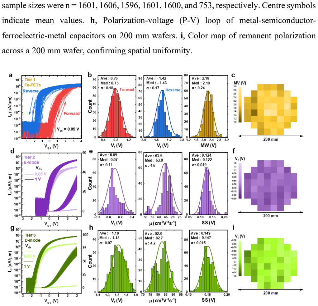
The paper's central claim is that wafer-scale monolithic 3D integration works with ALD-grown amorphous indium oxide channels. The authors show three tiers—Fe-FETs at the bottom, enhancement-mode FETs in the middle, and depletion-mode FETs on top—all fabricated on the same 200 mm wafer, and they quantify uniformity across the wafer: threshold-voltage spreads down to $0.04$ V, memory windows averaging $2.18$ V, and mobilities of $63.5$ to $91.6\ \mathrm{cm^2\,V^{-1}s^{-1}}$ depending on tier and thickness. The top-tier devices show no degradation relative to the bottom tier, which is the prerequisite for stacking more tiers. With the same three tiers, the paper demonstrates fully functional cross-tier circuits, so that logic and memory are not just co-located vertically but actually connected through inter-layer vias. The final claim is system-level: using a custom InOx process design kit and a three-dimensional design flow, a four-tier computing-in-memory accelerator for transformer-based LLMs partitions static weights into ferroelectric NVM and dynamic attention computations into eDRAM, and is projected to deliver $1.4\times$ to $2.9\times$ speedup and comparable energy-delay-product improvement over a same-footprint planar implementation.
Load-bearing premise
The load-bearing premise is that the custom simulation framework and process design kit, calibrated to measured single-tier devices, faithfully predict the performance of a four-tier chip that was never fabricated.
Editorial extensions
If this is right
- The 200 mm process establishes ALD InOx as a candidate BEOL channel with the uniformity ($V_{th}$ sigma down to 0.04 V) and yield needed for wafer-scale manufacturing.
- Cross-tier inverters, Fe-NVMs, and eDRAMs show that logic and memory can be interconnected vertically, not just stacked, so dense 3D systems-on-wafer become possible.
- Because the top-tier devices show no degradation, the same process can in principle be repeated to add a fourth, fifth, or more tiers.
- The CIM accelerator projection implies that splitting LLM workloads between static Fe-NVM and dynamic eDRAM tiers could cut inference latency by 1.4x to 2.9x relative to a planar implementation of the same footprint.
- NMOS-only logic built from E-mode and D-mode InOx FETs gives a complete standard-cell library, so existing 2D physical-design tools can be reused for a tier-by-tier 3D flow.
Reading between the lines
- The four-tier CIM speedup is a simulation result, not a measured chip; until a four-tier part is fabricated and benchmarked, the 1.4x to 2.9x range should be treated as a calibrated projection rather than a demonstrated speedup.
- If the wafer-level uniformity and cross-tier yields reproduce in a commercial fab, ALD InOx M3D could lower the cost of 3D integration relative to wafer bonding, because it avoids high-temperature epitaxy and transfer steps.
- The multi-level Fe-NVM cell stores n voltage levels times m polarization states; testing whether these levels stay separable under cycling, retention, and read disturb would directly probe whether that extra dimension is practical for analog in-memory computing.
- Because the authors note the layout is not yet optimized for parasitic capacitance and coupling, reducing those parasitics should improve cross-tier circuit margins and may push the projected speedup beyond the lower bound.
Editorial analysis
A structured set of objections, weighed in public.
Referee Report
Summary. This paper reports wafer-scale monolithic 3D (M3D) integration of three tiers of atomic-layer-deposited (ALD) InOx-based devices on 200 mm silicon wafers, including ferroelectric (Fe-FET), enhancement-mode (E-mode), and depletion-mode (D-mode) field-effect transistors. The authors present statistical characterization of over 100,000 fabricated devices, achieving threshold-voltage standard deviation as low as 0.04 V, average mobility up to 91.6 cm2/V·s, and fully functional cross-tier circuits including multi-level ferroelectric nonvolatile memories (MLFe-NVMs), inverters, and 2T0C eDRAMs. The paper also describes a four-tier 3D computing-in-memory (CIM) accelerator design for large-language-model workloads, implemented with a custom InOx process design kit and evaluated with an in-house simulation framework, with a claimed 1.4x to 2.9x speedup and comparable energy-delay-product improvements over a same-footprint 2D baseline.
Significance. If the experimental claims are confirmed, this work represents a notable advance in BEOL-compatible M3D integration. The paper's main strength is the substantial statistical data: more than 300 devices per tier across 52 dies, wafer-scale Vth maps, and functional cross-tier circuits, which support the scalability and uniformity claims. The CIM accelerator projection is forward-looking but is a simulation-based case study rather than a fabricated chip; its credibility rests on the calibration of the custom PDK and the fairness of the baseline, both of which require more transparency. The explicit limitation statement in the Conclusions is a positive sign, but the abstract's unqualified 'delivering' overstates the evidence.
major comments (4)
- [Abstract; 'Indium oxide multi tier computing in memory accelerator'] The 1.4–2.9x speedup claim is a projected simulation result from an in-house framework (3D-CIMlet, ref. 55) and a custom OS-PDK, not a measurement of a fabricated four-tier chip. The abstract's wording 'delivering' should be qualified as 'projected' or 'simulated' to avoid overstating the evidence. Furthermore, the Methods define the 2D baseline as 'a planar oxide-semiconductor implementation constrained to the same chip footprint, FeFET/eDRAM composition ratio, and workload-mapping strategy.' Because the 3D macro stacks four tiers, this same-footprint constraint gives the 3D design roughly four times the active device area; the speedup therefore reflects at least in part increased resource density rather than an intrinsic per-device performance advantage. Please present a resource-matched comparison (e.g., equal total device area or equal memory capacity) or explicitly discuss the sensitivity of the speedup to this baseline definition.
- [Methods, 'System simulation and benchmarking'] The OS-PDK is calibrated from measured devices with channel lengths of 5 um (Fig. 2e) and 100 nm (Fig. 2a), yet the CIM design is implemented at the 40 nm technology node. The scaling methodology used to extrapolate the Verilog-A models from the measured devices to 40 nm (e.g., constant-field scaling, adjustment of mobility, Vth, and parasitic capacitances) is not described. Since the projected speedup and EDP depend on these scaled parameters, please provide the scaling rules or perform a sensitivity analysis over the assumed 40 nm device parameters.
- [Device characterizations of multi-tier ALD InOx transistors (Fig. 3)] The statement that 'the devices fabricated on the top tiers exhibit no performance degradation compared to those on the lower tiers' is not supported by a controlled comparison. The Tier-1 devices are Fe-FETs with HZO dielectric and 400°C annealing, Tier-2 devices are E-mode FETs, and Tier-3 devices are D-mode FETs with a thicker InOx channel; these differ in device type, dielectric, and channel thickness, so the observed differences in Vth and mobility cannot isolate the effect of tier level. A direct comparison of the same device type fabricated at Tier 1 and Tier 3 would substantiate the thermal-budget compatibility claim; otherwise the claim should be softened to 'remain functional.'
- [Cross tier integrated circuits and memory; 'Indium oxide multi tier computing in memory accelerator'] The eDRAM is described as 'refresh-free' with 'ultra-long retention,' but no quantitative retention time is reported in the main text. The retention characteristic in Fig. 4j shows a large on/off ratio, but the time scale and the criterion for a valid logic '1' are not stated. Please report the measured retention time (e.g., the time for the read current to degrade to a specified sense margin) and specify the refresh-free condition used in the CIM design.
minor comments (5)
- [Fig. 2c caption] The list of sample sizes (n = 19, 19, 21, 20, ...) would be clearer if the corresponding channel lengths were explicitly mapped in the caption, as the current list is ambiguous without the figure.
- [Abstract and introduction] The terms 'E-mode' and 'D-mode' are used without definition; please define them as enhancement-mode (normally off) and depletion-mode (normally on) at first use.
- [Conclusions; Methods, 'System simulation and benchmarking'] The paper notes that heat transport cannot be inferred directly from two-dimensional circuits, yet the system-level simulation does not include thermal effects; please state the thermal assumptions (e.g., uniform temperature, no inter-tier thermal coupling) in the simulation section.
- [Cross tier integrated circuits and memory] The MLFe-NVM description mentions 'n x m storage levels' but does not specify the demonstrated n and m values for the multi-level operation in Figs. 4b-4c; please clarify the number of distinct levels achieved.
- [References] Some references have inconsistent formatting (e.g., conference series names and years); please check for consistency (e.g., refs. 35, 38, 40).
Circularity Check
Experimental wafer-scale M3D integration is self-contained and not circular; the abstract's CIM speedup, however, is a projection from the authors' own in-house framework and a self-defined same-footprint 2D baseline, making the system-level claim self-referential.
-
self citation load bearing
[Abstract; Section 'Indium oxide multi tier computing in memory accelerator'; Methods, 'System simulation and benchmarking']
"The LLM accelerator is evaluated using our in-house framework55, which performs comprehensive model-to-chip mapping by processing detailed model parameters, chip configuration settings, and calibrated M3D technology libraries. ... The 2D baseline was a planar oxide-semiconductor implementation constrained to the same chip footprint, FeFET/eDRAM composition ratio, and workload-mapping strategy as the 3D design."
The headline 'delivering 1.4x to 2.9x speedup' is not a measured hardware result: it is an output of the authors' own 3D-CIMlet framework (ref. 55, whose authors overlap with the present paper) fed by a custom InOx PDK calibrated to the authors' devices. Because the 3D macro has four vertical tiers while the 2D baseline is a planar implementation constrained to the same footprint, the comparison builds the multi-tier resource-density advantage into the baseline definition.
full rationale
The core of the paper—200 mm wafer-scale fabrication of three-tier ALD InOx FETs and Fe-FETs, >100,000 devices, statistical Vth/mobility distributions, and functional cross-tier MLFe-NVMs, inverters, and 2T0C eDRAMs—is experimental and internally consistent. Device parameters are extracted by standard constant-current and maximum-transconductance methods, and the wafer-scale maps are direct measurements, so no derivation step reduces to its inputs. The only load-bearing self-reference is the system-level CIM evaluation: the 1.4x-2.9x speedup is produced by the authors' in-house framework55 and a custom PDK, with a 2D baseline that is defined by the authors to have the same footprint but only a single planar tier. That formulation intentionally isolates 'resource density and data movement,' so the speedup is partly an artifact of the chosen baseline rather than an externally validated performance-per-resource gain. This is a self-referential modeling claim, not a mathematical tautology, and the conclusion itself asks for larger hardware demonstrations. Because the central M3D integration claim has independent experimental content, the score is 4 rather than 6 or higher.
Assumptions & free parameters
free parameters (2)
- InOx channel thickness =
1.8 nm (thin, E-mode), 3.5 nm (thick, D-mode)
- Annealing temperature =
190-300 C in O2, plus 400 C N2 for HZO activation
assumptions (4)
- domain assumption ALD InOx deposited at 225 C is a high-quality channel with low defect density and good interface to HfO2 and HZO.
- domain assumption HZO on InOx crystallizes into the ferroelectric phase after 400 C N2 anneal without an interfacial layer.
- ad hoc to paper Verilog-A models and the OS-PDK calibrated from the fabricated devices are representative of a real 40 nm 3D chip.
- ad hoc to paper A 2D baseline with the same footprint and NVM/eDRAM composition ratio is a fair comparison for quantifying the M3D benefit.
Cite this review
Pith. "Pith review of 200 mm Wafer-Scale Monolithic 3D Integration of Atomic Layer-Deposited Oxide Semiconductors." pith.science (2026). https://pith.science/paper/2ESRA3EP
@misc{pith2026260809508,
  author       = {Pith},
  title        = {Pith review of: 200 mm Wafer-Scale Monolithic 3D Integration of Atomic Layer-Deposited Oxide Semiconductors},
  year         = {2026},
  howpublished = {\url{https://pith.science/paper/2ESRA3EP}},
  note         = {Machine review of arXiv:2608.09508}
}
read the original abstract
Monolithic 3D (M3D) integration offers a pathway to overcome the scaling limits of conventional silicon complementary metal-oxide-semiconductor (CMOS) technology by extending dense vertical stacking of multifunctional logic and memory devices. Here, we demonstrate wafer-scale M3D integration of three tiers of atomic-layer-deposited (ALD) indium oxide (InOx)-based devices (>100,000 fabricated), including ferroelectric, enhancement-mode, and depletion-mode field-effect transistors, on 200 mm silicon wafers. We achieve threshold voltage standard deviation as low as 0.04 V, average electron mobility up to 91.6 cm2V-1s-1, and fully functional cross-tier circuits. A four-tier 3D computing-in-memory (CIM) accelerator targeting large language model workloads is developed using a custom InOx process design kit, delivering 1.4x to 2.9x speedup and comparable energy-delay product improvements over 2D baselines. These results establish ALD InOx M3D integration as a scalable and CMOS-compatible platform for next-generation artificial intelligence hardware and advanced electronics.
Figures


Figures from the paper (2 more)


Reference graph
Works this paper leans on
- [1]
-
[2]
Wan, W. et al. A compute-in-memory chip based on resistive random-access memory. Nature 608, 504–512 (2022)
work page 2022
- [3]
-
[4]
Xiang, C. et al. 3D integration enables ultralow -noise isolator-free lasers in silicon photonics. Nature 620, 78–85 (2023)
work page 2023
- [5]
-
[6]
Bishop, M. D., Wong, H. S. P., Mitra, S. & Shulaker, M. M. Monolithic 3 -D Integration. IEEE Micro 39, 16–27 (2019)
work page 2019
-
[7]
Jayachandran, D. et al. Three-dimensional integration of two -dimensional field - effect transistors. Nature 625, 276–281 (2024)
work page 2024
-
[8]
Ghosh, S. et al. Monolithic and heterogeneous three-dimensional integration of two- dimensional materials with high-density vias. Nat. Electron. 7, 892–903 (2024)
work page 2024
Show all 59 references
-
[9]
Kim, K.S. et al. Growth-based monolithic 3D integration of single -crystal 2D semiconductors. Nature 636, 615–621 (2024)
2024
-
[10]
Lu, D. et al. Monolithic three-dimensional tier-by-tier integration via van der Waals lamination. Nature 630, 340–345 (2024). 25
2024
-
[12]
Sun, Y. et al. BEOL Three -Dimensional Stackable Oxide Semiconductor CMOS Inverter with a High Voltage Gain of 233 at Cryogenic Temperatures. Nano Lett. (2024) doi:10.1021/acs.nanolett.4c04701
2024 doi
-
[13]
Datta, S. et al. Back-End-of-Line Compatible Transistors for Monolithic 3 -D Integration. IEEE micro 39, 8-15 (2019)
2019
-
[14]
& Datta, S
Salahuddin, S., Ni, K. & Datta, S. The era of hyper -scaling in electronics. Nat. Electron. 1, 442–450 (2018)
2018
-
[15]
Li, S. et al. Nanometer-thin indium tin oxide for advanced high -performance electronics. Nat. Mater. 18, 1091–1097 (2019)
2019
-
[16]
Zhu, J. et al. Low-thermal-budget synthesis of monolayer molybdenum disulfide for silicon back-end-of-line integration on a 200 mm platform. Nat. Nanotechnol. 18, 456–463 (2023)
2023
-
[17]
Yuvaraja, S. et al. Three-dimensional integrated metal -oxide transistors. Nat. Electron. 7, 768–776 (2024)
2024
-
[18]
& Gong, X
Han, K., Kang, Y., Chen, X., Chen, Y. & Gong, X. Indium -Tin-Oxide Thin-Film Transistors with High Field -Effect Mobility (129.5 cm 2/V⋅s) and Low Thermal Budget (150 °C). IEEE Electron Device Letters 44, 1999–2002 (2023)
2023
-
[19]
Gong, X. et al. Reconfigurable 3D stacked oxide semiconductor devices for hybrid in-memory computing. Preprint at https://doi.org/10.21203/rs.3.rs -5138544/v1 (2024)
2024 doi
-
[20]
Si, M. et al. Why In2O3 Can Make 0.7 nm Atomic Layer Thin Transistors. Nano Lett. 21, 500–506 (2021)
2021
-
[21]
Si, M. et al. Scaled indium oxide transistors fabricated using atomic layer deposition. Nat. Electron. 5, 164–170 (2022)
2022
-
[24]
Liu, S. et al. Edge Continual Training and Inference with RRAM-Gain Cell Memory Integrated on Si CMOS. in IEEE International Electron Devices Meeting (IEDM) (2024). doi:10.1109/IEDM50854.2024.10873546
2024
-
[25]
Lin, Z. et al. Nanometer-Thick Oxide Semiconductor Transistor with Ultra -High Drain Current. ACS Nano 16, 21536–21545 (2022)
2022
-
[26]
Zhang, Z. et al. Ultrahigh Bias Stability of ALD In 2O3 FETs Enabled by High Temperature O2 Annealing. in IEEE Symposium on VLSI Technology and Circuits , (2023)
2023
-
[27]
Matsuda, S. et al. 30-nm-channel-length c -axis aligned crystalline In -Ga-Zn-O transistors with low off-state leakage current and steep subthreshold characteristics. in IEEE Symposium on VLSI Technology and Circuits, T216–T217 (2015)
2015
-
[28]
Niu, C. et al. Record-Low Metal to Semiconductor Contact Resistance in Atomic - Layer-Deposited In 2O3 TFTs Reaching the Quantum Limit. in IEEE International Electron Devices Meeting (IEDM) (2023). doi:10.1109/IEDM45741.2023.10413708
2023
-
[29]
Niu, C. et al. Surface Accumulation Induced Negative Schottky Barrier and Ultralow Contact Resistance in Atomic -Layer-Deposited In 2O3 Thin-Film Transistors. IEEE Trans Electron Devices 71, 3403–3410 (2024)
2024
-
[30]
Lin, Z. et al. High-Peformance BEOL-Compatible Atomic-Layer-Deposited In 2O3 Fe-FETs Enabled by Channel Length Scaling down to 7 nm: Achieving Performance Enhancement with Large Memory Window of 2.2 V, Long Retention > 10 years and High Endurance > 10 8 Cycles. in IEEE Interna...
2021
-
[31]
Huyghebaert, C. et al. 2D materials: Roadmap to CMOS integration. in IEEE International Electron Devices Meeting (IEDM), 22.1.1-22.1.4 (2018)
2018
-
[32]
Samavedam, S. B. et al. Future logic scaling: Towards atomic channels and deconstructed chips. in IEEE International Electron Devices Meeting (IEDM), 1.1.1- 1.1.10 (2020). 27
2020
-
[33]
Shi, Y. et al. Superior electrostatic control in uniform monolayer MoS 2 scaled transistors via in-situ surface smoothening. in IEEE International Electron Devices Meeting (IEDM) 37.1.1-37.1.4 (2021)
2021
-
[34]
Chiang, K.H. et al. Integration of 0.75 V VDD oxide-semiconductor 1T1C memory with advanced logic for an ultra -low-power low -latency cache solution. in IEEE Symposium on VLSI Technology and Circuits, (2025)
2025
-
[35]
Zhao, Y. et al. Revealing the Partially Coherent Nature of Transport in IGZO. arXiv preprint, arXiv:2512.21945 (2025)
2025
-
[36]
Liu, A. et al. Selenium-alloyed tellurium oxide for amorphous p -channel transistors. Nature 629, 798–802 (2024)
2024
-
[37]
Kwon, J. et al. 200-mm-wafer-scale integration of polycrystalline molybdenum disulfide transistors. Nat. Electron. 7, 356–364 (2024)
2024
-
[38]
Schram, T. et al. Integration and electrical evaluation of WS 2 and MoS2 FETs in a 300 mm pilot line. Discover Electronics, 3, 15 (2026)
2026
-
[39]
Dorow, C.J. et al. Exploring manufacturability of novel 2D channel materials: 300 mm wafer -scale 2D NMOS & PMOS using MoS 2, WS 2, & WSe 2. in IEEE International Electron Devices Meeting (IEDM), (2023)
2023
-
[40]
Mitard, J. et al. sub-40mV sigma VTH IGZO nFETs in 300mm fab. Electrochemical Society Transactions prime, 98, 205-217 (2020)
2020
-
[41]
Asselberghs, I. et al. Wafer-scale integration of double gated WS 2-transistors in 300mm Si CMOS fab. in IEEE International Electron Devices Meeting (IEDM), 40- 2 (2020)
2020
-
[42]
Qin, B. et al. Two-dimensional indium selenide wafers for integrated electronics Science, 389, 299-302 (2025)
2025
-
[43]
Lee, J. et al. Monolithic 3D integration of dual -gated ALD oxide -channel non - volatile capacitive memory on 40nm Si CMOS for digital compute -in-memory. in IEEE International Electron Devices Meeting (IEDM), (2025)
2025
-
[44]
Kang, JH. et al. Monolithic 3D integration of 2D materials-based electronics towards ultimate edge computing solutions. Nat. Mater. 22, 1470–1477 (2023)
2023
-
[45]
Pendurthi, R. et al. Monolithic three-dimensional integration of complementary two- dimensional field-effect transistors. Nat. Nanotechnol. 19, 970–977 (2024). 28
2024
-
[46]
Liu, C. et al. A full-featured 2D flash chip enabled by system integration. Nature 646, 1081–1088 (2025)
2025
-
[47]
Hills, G. et al. Modern microprocessor built from complementary carbon nanotube transistors. Nature 572, 595–602 (2019)
2019
-
[48]
Wang, Q. et al. Wafer-scale highly oriented monolayer MoS 2 with large domain sizes. Nano letters, 20, 7193-7199 (2020)
2020
-
[49]
Li, T. et al. Epitaxial growth of wafer -scale molybdenum disulfide semiconductor single crystals on sapphire. Nat. Nanotechnol. 16, 1201–1207 (2021)
2021
-
[50]
Lin, Z. et al. Enhancement of In2O3 Field-Effect Mobility Up To 152 cm2V-1s-1 Using HZO-Based Higher-k Linear Dielectric. in IEEE Symposium on VLSI Technology and Circuits, (2024)
2024
-
[51]
Si, M. et al. Enhancement-mode atomic -layer-deposited In 2O3 transistors with maximum drain current of 2.2 A/mm at drain voltage of 0.7 V by low -temperature annealing and stability in hydrogen environment. IEEE Transactions on Electron Devices, 68, 1075-1080 (2021)
2021
-
[52]
Li, S. et al. Nanometre-thin indium tin oxide for advanced high -performance electronics. Nat. Mater. 18, 1091–1097 (2019)
2019
-
[53]
Zhang, J. et al. Effects of Gallium on Electron Transport and Bias Stability in Ultrascaled Amorphous InGaO Transistors. IEEE Transactions on Electron Devices, 72, 4156-4162 (2025)
2025
-
[54]
Park, H. et al. Extreme EOT Scaling in Tungsten -Doped In 2O3 MOSFETs for Enhanced Stability and Drive Current. IEEE Transactions on Electron Devices , 72, 7136-7144 (2025)
2025
-
[55]
Du, S. et al. 3D-CIMlet: A Chiplet Co -Design Framework for Heterogeneous In - Memory Acceleration of Edge LLM Inference and Continual Learning. in IEEE Design Automation Conference (2025)
2025
-
[56]
Vaswani, A. et al. Attention is All you Need. Advances in neural information processing systems 30 (2017)
2017
-
[57]
-W., Lee, K
Devlin, J., Chang, M. -W., Lee, K. & Toutanova, K. Bert: Pre -training of deep bidirectional transformers for language understanding. in Proceedings of the 2019 conference of the North American chapter of the association for computational linguistics: human language technologi...
2019
-
[58]
Radford, A. et al. Language models are unsupervised multitask learners. OpenAI blog 1, 8 (2019)
2019
-
[59]
Touvron, H. et al. Training data-efficient image transformers & distillation through attention. In International conference on machine learning 10347-10357 (2021)
2021
-
[60]
Ao, M. et al. A RISC -V 32 -bit microprocessor based on two -dimensional semiconductors. Nature 640, 654–661 (2025)
2025
-
[61]
Yakubo, Y. et al. Crystalline oxide semiconductor-based 3D bank memory system for endpoint artificial intelligence with multiple neural networks facilitating context switching and power gating. in IEEE International Solid-State Circuits Conference (ISSCC), (2023)
2023
-
[62]
Liu, S. et al. Edge continual training and inference with RRAM -gain cell memory integrated on Si CMOS. in IEEE International Electron Devices Meeting (IEDM) , (2024)
2024
Reviewed August 11, 2026 · model on record in the stance chip above.
Discussion (0). Continue with ORCID to comment.