Fabrication of high-quality topological insulator nanodevices from bulk-insulating air-sensitive Sb-Bi₂Se₃
Pith reviewed 2026-07-03 18:33 UTC · model grok-4.3
The pith
Room-temperature fabrication protocol preserves the low carrier density of exfoliated Sb-Bi2Se3 in Hall bar and nanowire devices.
A machine-rendered reading of the paper's core claim, the machinery that carries it, and where it could break.
Core claim
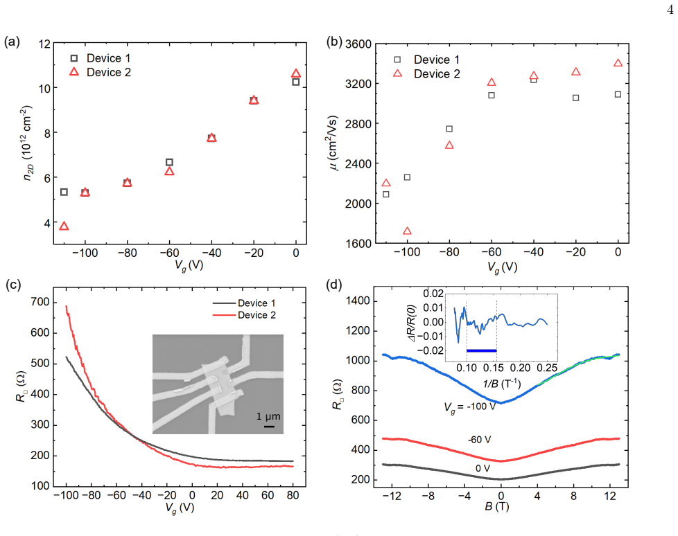
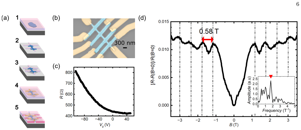
The authors establish that a room-temperature fabrication protocol maintains the low bulk carrier density of air-sensitive Sb-Bi2Se3 when fabricating Hall bar and nanowire devices, as indicated by the observation of quantum interference oscillations in nanowires, a large gate tunability, and clear signatures of weak antilocalization.
What carries the argument
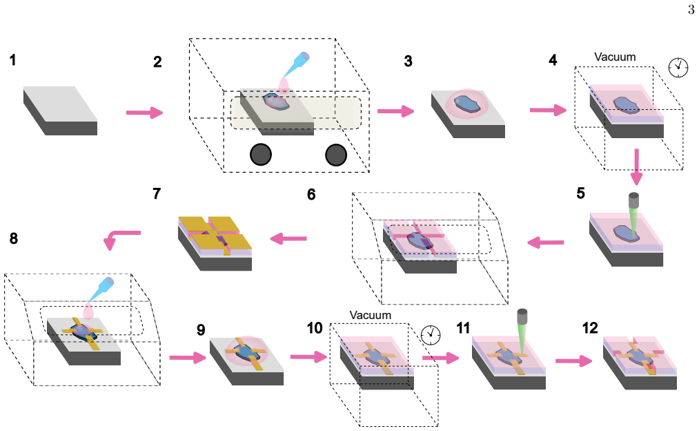
Room-temperature fabrication protocol that avoids thermal processing during microfabrication of exfoliated flakes.
If this is right
- Nanowire devices display quantum interference oscillations.
- Fabricated devices exhibit large gate tunability.
- Clear weak antilocalization signatures appear in the transport data.
- The resulting devices qualify as high-quality platforms for topological insulator-superconductor hybrid studies.
Where Pith is reading between the lines
- The same avoidance of heat during processing could be tested on other air-sensitive topological materials to check whether low carrier density is retained.
- Direct comparison of carrier density before and after each fabrication step on the same flake would strengthen the evidence that no hidden surface or interface effects are at play.
- Extending the protocol to more complex geometries such as junctions could open routes to cleaner hybrid devices without added disorder.
Load-bearing premise
The transport signatures of quantum oscillations, gate tunability, and weak antilocalization directly confirm that bulk carrier density stays low without fabrication-induced changes.
What would settle it
Measurement of substantially higher carrier density or complete absence of quantum interference oscillations and weak antilocalization in the completed Hall bars and nanowires compared with the starting exfoliated flakes would show the protocol failed to preserve the properties.
Figures
read the original abstract
High-quality topological insulator (TI) materials are essential for the realization and detection of Majorana bound states (MBSs) in TI-superconductor hybrid platforms. Widely used compensated TIs exhibit substantial disorder and charge inhomogeneity, which may be detrimental for Majorana devices. In this regard, Sb-substituted Bi$_2$Se$_3$ (SBS) is promising, because it is non-compensated and yet achieves very low bulk carrier density. We systematically investigate the impact of thermal processing during microfabrication on the transport properties of SBS. We developed a room-temperature fabrication protocol that preserves the low carrier density of exfoliated SBS upon fabrication of Hall bar and nanowire devices as evidenced from the observation of quantum interference oscillations in nanowires, a large gate tunability, and clear signatures of weak antilocalization (WAL).
Editorial analysis
A structured set of objections, weighed in public.
Referee Report
Summary. The manuscript reports development of a room-temperature microfabrication protocol for air-sensitive Sb-substituted Bi₂Se₃ (SBS) that is claimed to preserve the low bulk carrier density of exfoliated flakes when fabricating Hall bars and nanowires. Preservation is asserted on the basis of observed quantum interference oscillations in nanowires, large gate tunability, and clear weak antilocalization (WAL) signatures.
Significance. A fabrication method that reliably maintains the low bulk doping and surface-state dominance of compensated-free TIs such as SBS would be useful for hybrid TI-superconductor devices targeting Majorana states, where bulk conduction and disorder are known obstacles. The room-temperature approach avoids thermal degradation steps that commonly affect air-sensitive TIs.
major comments (1)
- [Abstract] Abstract: the central claim that quantum interference oscillations, gate tunability, and WAL constitute direct evidence of preserved low bulk carrier density is not load-bearing. These features are generic to TI surface states and can appear in thin nanowires or gated Hall bars even when fabrication increases bulk density (via defects or oxidation), because surface-to-volume ratio favors surface conduction. No pre- versus post-fabrication Hall density comparison or temperature-activated bulk resistivity data are referenced to exclude this alternative.
Simulated Author's Rebuttal
We thank the referee for the constructive review of our manuscript. We respond to the major comment below.
read point-by-point responses
-
Referee: [Abstract] Abstract: the central claim that quantum interference oscillations, gate tunability, and WAL constitute direct evidence of preserved low bulk carrier density is not load-bearing. These features are generic to TI surface states and can appear in thin nanowires or gated Hall bars even when fabrication increases bulk density (via defects or oxidation), because surface-to-volume ratio favors surface conduction. No pre- versus post-fabrication Hall density comparison or temperature-activated bulk resistivity data are referenced to exclude this alternative.
Authors: We agree that quantum interference oscillations, gate tunability, and WAL are generic signatures of surface-state transport in TIs and do not by themselves constitute direct quantitative evidence that bulk carrier density is unchanged from the starting exfoliated flakes. These features can persist even if fabrication introduces some additional bulk doping, provided the surface-to-volume ratio remains favorable. Our manuscript's central point is instead the systematic comparison showing that thermal processing steps degrade these signatures while the room-temperature protocol maintains them at levels comparable to unprocessed flakes. We will revise the abstract to replace 'as evidenced from' with language indicating that the observations are 'consistent with' preservation of low bulk density. We will also add a sentence noting the indirect nature of the evidence and the absence of direct pre/post Hall density comparisons in the current data set. revision: partial
Circularity Check
No circularity: purely experimental report with direct measurements
full rationale
This is an experimental fabrication and transport study with no derivations, equations, fitted parameters, or theoretical chains. The central claim rests on observed quantum interference oscillations, gate tunability, and WAL signatures in fabricated devices, which are presented as direct empirical evidence rather than predictions derived from inputs. No self-citations are load-bearing for any derivation, and no ansatz or uniqueness theorems are invoked. The paper is self-contained against external benchmarks via standard transport measurements.
Axiom & Free-Parameter Ledger
Reference graph
Works this paper leans on
-
[1]
Fu and C
L. Fu and C. L. Kane, Superconducting proximity effect and Majorana fermions at the surface of a topological insulator, Phys. Rev. Lett.100, 096407 (2008)
2008
-
[2]
Hosur, P
P. Hosur, P. Ghaemi, R. S. K. Mong, and A. Vishwanath, Majorana modes at the ends of superconductor vortices in doped topological insulators, Phys. Rev. Lett.107, 097001 (2011)
2011
-
[3]
Cook and M
A. Cook and M. Franz, Majorana fermions in a topological-insulator nanowire proximity-coupled to an s-wave superconductor, Phys. Rev. B84, 201105 (2011)
2011
-
[4]
A. M. Cook, M. M. Vazifeh, and M. Franz, Stability of Majorana fermions in proximity-coupled topological in- 8 sulator nanowires, Phys. Rev. B86, 155431 (2012)
2012
-
[5]
Takei, B
S. Takei, B. M. Fregoso, H.-Y. Hui, A. M. Lobos, and S. Das Sarma, Soft superconducting gap in semiconduc- tor Majorana nanowires, Phys. Rev. Lett.110, 186803 (2013)
2013
-
[6]
S. Ahn, H. Pan, B. Woods, T. D. Stanescu, and S. Das Sarma, Estimating disorder and its adverse ef- fects in semiconductor Majorana nanowires, Phys. Rev. Mater.5, 124602 (2021)
2021
-
[7]
Adagideli, M
I. Adagideli, M. Wimmer, and A. Teker, Effects of electron scattering on the topological properties of nanowires: Majorana fermions from disorder and super- lattices, Phys. Rev. B89, 144506 (2014)
2014
-
[8]
Kaufhold and A
L. Kaufhold and A. Rosch, Stability of Majorana modes in Coulomb-disordered topological insulator nanowires, Phys. Rev. B112, 045310 (2025)
2025
-
[9]
Das Sarma and H
S. Das Sarma and H. Pan, Disorder-induced zero-bias peaks in Majorana nanowires, Phys. Rev. B103, 195158 (2021)
2021
-
[10]
Ando, Topological insulator materials, Journal of the Physical Society of Japan82, 102001 (2013)
Y. Ando, Topological insulator materials, Journal of the Physical Society of Japan82, 102001 (2013)
2013
-
[11]
Borgwardt, J
N. Borgwardt, J. Lux, I. Vergara, Z. Wang, A. A. Taskin, K. Segawa, P. H. M. van Loosdrecht, Y. Ando, A. Rosch, and M. Gr¨ uninger, Self-organized charge puddles in a three-dimensional topological material, Phys. Rev. B93, 245149 (2016)
2016
-
[12]
Zhang, C.-X
H. Zhang, C.-X. Liu, X.-L. Qi, X. Dai, Z. Fang, and S.- C. Zhang, Topological insulators in Bi 2Se3, Bi 2Te3 and Sb2Te3 with a single dirac cone on the surface, Nature Physics5, 438–442 (2009)
2009
-
[13]
Navr´ atil, J
J. Navr´ atil, J. Hor´ ak, T. Plech´ aˇ cek, S. Kamba, P. Loˇ st’´ ak, J. Dyck, W. Chen, and C. Uher, Conduc- tion band splitting and transport properties of Bi 2Se3, Journal of Solid State Chemistry177, 1704 (2004)
2004
-
[14]
Y. S. Hor, A. Richardella, P. Roushan, Y. Xia, J. G. Checkelsky, A. Yazdani, M. Z. Hasan, N. P. Ong, and R. J. Cava,p-type Bi 2Se3 for topological insulator and low-temperature thermoelectric applications, Phys. Rev. B79, 195208 (2009)
2009
-
[15]
J. G. Analytis, J.-H. Chu, Y. Chen, F. Corredor, R. D. McDonald, Z. X. Shen, and I. R. Fisher, Bulk fermi surface coexistence with dirac surface state in Bi 2Se3: A comparison of photoemission and shubnikov–de haas measurements, Phys. Rev. B81, 205407 (2010)
2010
-
[16]
J. A. Sobota, S. Yang, J. G. Analytis, Y. L. Chen, I. R. Fisher, P. S. Kirchmann, and Z.-X. Shen, Ultrafast opti- cal excitation of a persistent surface-state population in the topological insulator Bi 2Se3, Phys. Rev. Lett.108, 117403 (2012)
2012
-
[17]
J. G. Analytis, R. D. McDonald, S. C. Riggs, J.-H. Chu, G. S. Boebinger, and I. R. Fisher, Two-dimensional sur- face state in the quantum limit of a topological insulator, Nature Physics6, 960–964 (2010)
2010
-
[18]
J. G. Checkelsky, Y. S. Hor, R. J. Cava, and N. P. Ong, Bulk band gap and surface state conduction observed in voltage-tuned crystals of the topological insulator Bi2Se3, Phys. Rev. Lett.106, 196801 (2011)
2011
-
[19]
Bianchi, R
M. Bianchi, R. C. Hatch, J. Mi, B. B. Iversen, and P. Hof- mann, Simultaneous quantization of bulk conduction and valence states through adsorption of nonmagnetic impu- rities on Bi 2Se3, Phys. Rev. Lett.107, 086802 (2011)
2011
-
[20]
D. Kong, J. J. Cha, K. Lai, H. Peng, J. G. Analytis, S. Meister, Y. Chen, H.-J. Zhang, I. R. Fisher, Z.-X. Shen, and Y. Cui, Rapid surface oxidation as a source of surface degradation factor for Bi 2Se3, ACS Nano5, 4698–4703 (2011)
2011
-
[21]
L. V. Yashina, J. S´ anchez-Barriga, M. R. Scholz, A. A. Volykhov, A. P. Sirotina, S. Neudachina, Vera, M. E. Tamm, A. Varykhalov, D. Marchenko, G. Springholz, G. Bauer, A. Knop-Gericke, and O. Rader, Negligi- ble surface reactivity of topological insulators Bi 2Se3 and Bi 2Te3 towards oxygen and water, ACS Nano7, 5181–5191 (2013)
2013
-
[22]
H. M. Benia, C. Lin, K. Kern, and C. R. Ast, Reac- tive chemical doping of the Bi 2Se3 topological insulator, Phys. Rev. Lett.107, 177602 (2011)
2011
-
[23]
V. A. Golyashov, K. A. Kokh, S. V. Makarenko, K. N. Romanyuk, I. P. Prosvirin, A. V. Kalinkin, O. E. Tereshchenko, A. S. Kozhukhov, D. V. Sheglov, S. V. Ere- meev, S. D. Borisova, and E. V. Chulkov, Inertness and degradation of (0001) surface of Bi 2Se3 topological insu- lator, Journal of Applied Physics112, 10.1063/1.4767458 (2012)
-
[24]
K. Park, C. D. Beule, and B. Partoens, The ageing ef- fect in topological insulators: evolution of the surface electronic structure of Bi 2Se3 upon K adsorption, New Journal of Physics15, 113031 (2013)
2013
-
[25]
A. J. Green, S. Dey, Y. Q. An, B. O’Brien, S. O’Mullane, B. Thiel, and A. C. Diebold, Surface oxidation of the topological insulator Bi 2Se3, Journal of Vacuum Sci- ence & Technology A: Vacuum, Surfaces, and Films34, 10.1116/1.4964637 (2016)
-
[26]
V. V. Atuchin, V. A. Golyashov, K. A. Kokh, I. V. Korolkov, A. S. Kozhukhov, V. N. Kruchinin, S. V. Makarenko, L. D. Pokrovsky, I. P. Prosvirin, K. N. Ro- manyuk, and O. E. Tereshchenko, Formation of inert Bi2Se3(0001) cleaved surface, Crystal Growth & Design 11, 5507–5514 (2011)
2011
-
[27]
C. R. Thomas, M. K. Vallon, M. G. Frith, H. Sezen, S. K. Kushwaha, R. J. Cava, J. Schwartz, and S. L. Bernasek, Surface oxidation of Bi 2(Te,Se) 3 topological insulators depends on cleavage accuracy, Chemistry of Materials28, 35–39 (2015)
2015
-
[28]
M. T. Edmonds, J. T. Hellerstedt, A. Tadich, A. Schenk, K. M. O’Donnell, J. Tosado, N. P. Butch, P. Syers, J. Paglione, and M. S. Fuhrer, Stability and surface re- construction of topological insulator Bi 2Se3 on exposure to atmosphere, The Journal of Physical Chemistry C 118, 20413–20419 (2014)
2014
-
[29]
S. S. Hong, J. J. Cha, D. Kong, and Y. Cui, Ultra- low carrier concentration and surface-dominant transport in antimony-doped Bi2Se3 topological insulator nanorib- bons, Nature Communications3, 10.1038/ncomms1771 (2012)
-
[30]
D. Kim, S. Cho, N. P. Butch, P. Syers, K. Kirshenbaum, S. Adam, J. Paglione, and M. S. Fuhrer, Surface con- duction of topological dirac electrons in bulk insulating Bi2Se3, Nature Physics8, 459–463 (2012)
2012
-
[31]
S. Cho, B. Dellabetta, A. Yang, J. Schneeloch, Z. Xu, T. Valla, G. Gu, M. J. Gilbert, and N. Mason, Symmetry protected josephson supercurrents in three- dimensional topological insulators, Nature Communica- tions4, 10.1038/ncomms2701 (2013)
-
[32]
S. Cho, B. Dellabetta, R. Zhong, J. Schneeloch, T. Liu, G. Gu, M. J. Gilbert, and N. Mason, Aharonov–bohm oscillations in a quasi-ballistic three-dimensional topo- logical insulator nanowire, Nature Communications6, 10.1038/ncomms8634 (2015). 9
-
[33]
Breunig and Y
O. Breunig and Y. Ando, Opportunities in topological insulator devices, Nature Reviews Physics4, 184–193 (2021)
2021
-
[34]
A. S. Mayorov, R. V. Gorbachev, S. V. Morozov, L. Brit- nell, R. Jalil, L. A. Ponomarenko, P. Blake, K. S. Novoselov, K. Watanabe, T. Taniguchi, and A. K. Geim, Micrometer-scale ballistic transport in encapsu- lated graphene at room temperature, Nano Letters11, 2396–2399 (2011)
2011
-
[35]
Salehi, M
M. Salehi, M. Brahlek, N. Koirala, J. Moon, L. Wu, N. P. Armitage, and S. Oh, Stability of low-carrier-density topological-insulator Bi 2Se3 thin films and effect of cap- ping layers, APL Materials3, 091101 (2015)
2015
-
[36]
S. Heedt, M. Quintero-P´ erez, F. Borsoi, A. Fursina, N. van Loo, G. P. Mazur, M. P. Nowak, M. Ammerlaan, K. Li, S. Korneychuk, J. Shen, M. A. Y. van de Poll, G. Badawy, S. Gazibegovic, N. de Jong, P. Aseev, K. van Hoogdalem, E. P. A. M. Bakkers, and L. P. Kouwen- hoven, Shadow-wall lithography of ballistic superconduc- tor–semiconductor quantum devices, ...
-
[37]
D. Kim, P. Syers, N. P. Butch, J. Paglione, and M. S. Fuhrer, Coherent topological transport on the surface of Bi2Se3, Nature Communications4, 10.1038/ncomms3040 (2013)
-
[38]
Ihn,Semiconductor Nanostructures: Quantum states and electronic transport(OUP Oxford, 2009)
T. Ihn,Semiconductor Nanostructures: Quantum states and electronic transport(OUP Oxford, 2009)
2009
-
[39]
F. Qu, C. Zhang, R.-R. Du, and L. Lu, Coexistence of bulk and surface shubnikov-de haas oscillations in Bi2Se3, Journal of Low Temperature Physics170, 397–402 (2012)
2012
-
[40]
A. S. Hewitt, J. Wang, J. Boltersdorf, P. A. Maggard, and D. B. Dougherty, Coexisting bi and se surface ter- minations of cleaved Bi 2Se3 single crystals, Journal of Vacuum Science &; Technology B, Nanotechnology and Microelectronics: Materials, Processing, Measurement, and Phenomena32, 10.1116/1.4873689 (2014)
-
[41]
Gauthier, J
A. Gauthier, J. A. Sobota, N. Gauthier, C. R. Rotundu, Z.-X. Shen, and P. S. Kirchmann, Band structure of bi surfaces formed on Bi 2Se3 upon exposure to air, Phys. Rev. Mater.8, 054201 (2024)
2024
-
[42]
F. M¨ unning, O. Breunig, H. F. Legg, S. Roitsch, D. Fan, M. R¨ oßler, A. Rosch, and Y. Ando, Quantum confine- ment of the dirac surface states in topological-insulator nanowires, Nature Communications12, 10.1038/s41467- 021-21230-3 (2021)
-
[43]
Kim, T.-H
H.-S. Kim, T.-H. Hwang, N.-H. Kim, Y. Hou, D. Yu, H.-S. Sim, and Y.-J. Doh, Adjustable quantum interfer- ence oscillations in sb-doped Bi2Se3 topological insulator nanoribbons, ACS Nano14, 14118–14125 (2020)
2020
-
[44]
H. Peng, K. Lai, D. Kong, S. Meister, Y. Chen, X.-L. Qi, S.-C. Zhang, Z.-X. Shen, and Y. Cui, Aharonov–bohm interference in topological insulator nanoribbons, Nature Materials9, 225–229 (2009)
2009
-
[45]
E. Nikodem, J. Schluck, H. F. Legg, M. Geier, M. Pa- paj, M. Bagchi, L. Fu, and Y. Ando, Topological in- sulator nano-squid: Flux-tunable platform for topolog- ical superconductivity (2025), arXiv:2412.07993 [cond- mat.mes-hall]
-
[46]
E. Nikodem, J. Schluck, M. Geier, M. Papaj, H. F. Legg, J. Feng, M. Bagchi, L. Fu, and Y. Ando, Tunable su- perconducting diode effect in a topological nano-squid, Science Advances11, 10.1126/sciadv.adw4898 (2025)
-
[47]
H. F. Legg, M. R¨ oßler, F. M¨ unning, D. Fan, O. Bre- unig, A. Bliesener, G. Lippertz, A. Uday, A. A. Taskin, D. Loss, J. Klinovaja, and Y. Ando, Giant magnetochi- ral anisotropy from quantum-confined surface states of topological insulator nanowires, Nature Nanotechnology 17, 696–700 (2022). Supplementary materials for ”Fabrication of high-quality topol...
2022
-
[48]
J. G. Checkelsky, Y. S. Hor, R. J. Cava, and N. P. Ong, Bulk band gap and surface state conduction observed in voltage-tuned crystals of the topological insulator Bi 2Se3, Phys. Rev. Lett.106, 196801 (2011)
2011
-
[49]
J. G. Analytis, R. D. McDonald, S. C. Riggs, J.-H. Chu, G. S. Boebinger, and I. R. Fisher, Two-dimensional surface state in the quantum limit of a topological insulator, Nature Physics 6, 960–964 (2010)
2010
-
[50]
Z. Ren, A. A. Taskin, S. Sasaki, K. Segawa, and Y. Ando, Large bulk resistivity and surface quantum oscillations in the topological insulator Bi2Se2Te, Phys. Rev. B82, 241306(R) (2010)
2010
-
[51]
H. Peng, K. Lai, D. Kong, S. Meister, Y. Chen, X.-L. Qi, S.-C. Zhang, Z.-X. Shen, and Y. Cui, Aharonov–bohm interference in topological insulator nanoribbons, Nature Materials9, 225–229 (2009). 11
2009
discussion (0)
Sign in with ORCID, Apple, or X to comment. Anyone can read and Pith papers without signing in.