Nanometric voids as optical antennas for rewritable momentum-engineered photonics in silicon
Pith reviewed 2026-06-30 01:55 UTC · model grok-4.3
The pith
Nanometric voids in crystalline silicon act as optical antennas that relax selection rules via dielectric discontinuity without foreign materials.
A machine-rendered reading of the paper's core claim, the machinery that carries it, and where it could break.
Core claim
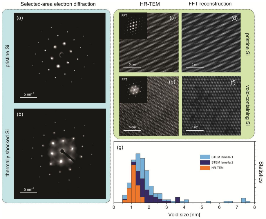
Nanometric voids embedded within crystalline silicon act as optical antennas, dramatically altering the optical response of an indirect semiconductor without the introduction of any foreign material. Using an electrically induced melt-quench process, the voids enable intense broadband photo- and electroluminescence spectrally indistinguishable from that produced by metallic or semiconductor nanoconfiners, establishing that dielectric discontinuity governs the momentum-assisted optical transitions. The luminescence can be repeatedly written, erased, and rewritten through alternating electrical conditioning and optical recrystallization.
What carries the argument
Nanometric voids as optical antennas, where dielectric discontinuity broadens the photon momentum distribution to relax optical selection rules.
If this is right
- Photonic functionality can be embedded and reconfigured directly within bulk silicon without adding foreign materials.
- The optical response of an indirect semiconductor can be altered solely by internal dielectric discontinuities.
- Luminescence intensity and spectrum are governed by void geometry and density rather than confiner composition.
- Repeated electrical and optical cycling allows the same silicon volume to be switched between luminescent and non-luminescent states.
Where Pith is reading between the lines
- The same void-based mechanism could be tested in other indirect semiconductors such as germanium to produce native-material light emitters.
- Because no foreign atoms are introduced, integration with conventional silicon electronics may avoid compatibility barriers that affect doped or hybrid devices.
- Systematic variation of void size and spacing could map how confinement scale controls the degree of momentum broadening.
Load-bearing premise
The observed luminescence arises specifically from momentum broadening due to dielectric discontinuity at the voids rather than from defects, strain, or other byproducts of the melt-quench process.
What would settle it
If silicon samples containing comparable defects and strain but lacking voids, or samples with voids whose dielectric contrast is removed, exhibit no comparable broadband luminescence, that would falsify the claim.
Figures


read the original abstract
Optical antennas are widely used to localize electromagnetic fields far below the diffraction limit, enabling enhanced light-matter interactions across nanophotonics. Yet the regime in which optical confinement approaches the electronic de Broglie wavelength in a solid - where the photon momentum distribution broadens sufficiently to relax optical selection rules - remains largely unexplored. Here we show that nanometric voids embedded within crystalline silicon act as such optical antennas, dramatically altering the optical response of an indirect semiconductor without the introduction of any foreign material. Using an electrically induced melt-quench process, we generate nanometric voids throughout bulk silicon, confirmed by high-resolution electron microscopy, diffraction analysis, Fourier-filtered lattice reconstruction, elemental mapping, and supported by optical and vibrational spectroscopies. The void-containing silicon exhibits intense broadband photo- and electroluminescence spectrally indistinguishable from that produced by metallic or semiconductor nanoconfiners of similar dimensions, establishing that dielectric discontinuity, not confiner composition, governs the observed momentum-assisted optical transitions. The luminescence can be repeatedly written, erased, and rewritten through alternating electrical conditioning and optical recrystallization. These findings establish nanometric voids as a previously unexplored platform for extreme optical confinement and demonstrate that photonic functionality can be embedded and reconfigured directly within bulk silicon.
Editorial analysis
A structured set of objections, weighed in public.
Referee Report
Summary. The manuscript claims that nanometric voids embedded in crystalline silicon via an electrically induced melt-quench process function as optical antennas. These voids broaden the photon momentum distribution through dielectric discontinuity at the void-silicon interface, enabling intense broadband photo- and electroluminescence in an indirect-bandgap material without foreign dopants or inclusions. The effect is supported by HRTEM, diffraction, elemental mapping, and optical/vibrational spectroscopies, shown to be spectrally equivalent to that from metallic or semiconductor nanoconfiners, and demonstrated to be repeatedly writable/erased via electrical conditioning and optical recrystallization.
Significance. If the attribution to voids is rigorously isolated, the result would establish a composition-independent route to extreme optical confinement and momentum relaxation directly inside bulk silicon, with implications for rewritable silicon photonics. The multi-technique characterization and external comparison to nanoconfiners are positive features; however, the absence of quantitative luminescence yields, error bars, or spectral overlap metrics in the provided abstract reduces the immediate assessability of the effect size.
major comments (1)
- [Abstract] Abstract and methods (process description): The central claim that luminescence arises specifically from dielectric discontinuity at the voids (rather than defects, strain, or other melt-quench byproducts) is load-bearing. The nanoconfiner comparison samples are fabricated by different routes, and no process-matched control (identical electrical/thermal history without void formation) is described. This leaves open the possibility that the observed optical response is induced by the conditioning process itself independent of voids.
Simulated Author's Rebuttal
We thank the referee for the detailed review and for highlighting the importance of rigorously isolating the role of voids. We address the major comment below and propose revisions to strengthen the manuscript.
read point-by-point responses
-
Referee: [Abstract] Abstract and methods (process description): The central claim that luminescence arises specifically from dielectric discontinuity at the voids (rather than defects, strain, or other melt-quench byproducts) is load-bearing. The nanoconfiner comparison samples are fabricated by different routes, and no process-matched control (identical electrical/thermal history without void formation) is described. This leaves open the possibility that the observed optical response is induced by the conditioning process itself independent of voids.
Authors: We agree that isolating the contribution of the voids is central. The manuscript already demonstrates that the luminescence is erased upon optical recrystallization (which removes the voids) and can be rewritten by re-applying the electrical conditioning, providing an internal control with matched process history but without voids. We will revise the methods and results sections to explicitly frame the recrystallized state as the process-matched control, include quantitative comparison of luminescence intensity before/after recrystallization, and add error bars where appropriate. For the nanoconfiner comparisons, while the fabrication routes differ, the spectral indistinguishability across metallic, semiconductor, and void cases supports that the effect originates from the dielectric discontinuity itself rather than composition-specific byproducts; we will expand the discussion to address potential route-dependent differences and note that the void samples use the same silicon host as the controls. revision: yes
Circularity Check
No circularity: experimental demonstration with independent controls and characterizations
full rationale
The paper is an experimental study that fabricates nanometric voids in silicon via melt-quench, characterizes them with HRTEM/diffraction/elemental mapping/optical spectroscopies, and reports luminescence comparable to external nanoconfiners. No equations, first-principles derivations, fitted parameters renamed as predictions, or self-citation chains appear in the provided text. The load-bearing attribution to dielectric discontinuity rests on direct experimental comparisons and multiple orthogonal techniques rather than any definitional or fitted reduction. The work is self-contained against external benchmarks.
Axiom & Free-Parameter Ledger
axioms (1)
- domain assumption Silicon possesses an indirect bandgap whose optical transitions require momentum conservation.
Reference graph
Works this paper leans on
-
[1]
1 Novotny, L. & van Hulst, N. Antennas for light. Nature Photonics 5, 83-90, doi:10.1038/nphoton.2010.237 (2011). 2 Bharadwaj, P., Deutsch, B. & Novotny, L. Optical Antennas. Advances in Optics and Photonics 1, 438-483, doi:10.1364/AOP.1.000438 (2009). 3 Biagioni, P., Huang, J.-S. & Hecht, B. Nanoantennas for visible and infrared radiation. Reports on Pro...
discussion (0)
Sign in with ORCID, Apple, or X to comment. Anyone can read and Pith papers without signing in.